Abstract
Complex materials have unique thermal and electron transport properties. In this work, a novel catalyst-assisted metal organic chemical vapor deposition approach was employed to make Bi-Te-Ni-Cu-Au complex materials on an anodic aluminum oxide nanoporous substrate. Nickel acetate, copper nitrate, bismuth acetate, and tellurium (IV) chloride dissolved in N,N-dimethylformamide (DMF) were used as the metal sources for Ni, Bi, Cu, and Te, respectively. Hydrogen was used as the carrier gas. The anodic aluminum oxide substrate sputter-coated on a thin gold coating and was kept at 500 °C in a quartz tube in the reaction chamber. The chemical vapor deposition time was two hours. Scanning electron microscopy was used to reveal the morphology of the deposited materials. Due to metal catalyst assisted growth, the Bi-Te-Ni-Cu-Au materials were self-assembled into islands distributed fairly uniformly on the substrate. The mechanism for the morphological development of the materials was investigated. It was found that the Au nanoparticles facilitated the formation of the complex Bi-Te-Al-Ni-Cu materials. The prepared nanostructure has the highest absolute Seekbeck coefficient value of 260 µV/K, which is more than twice the value obtained from the bulk material.
1. Introduction
Chemical vapor deposition (CVD) has been considered as a standard industrial coating technique since the 1970s. During the last two decades, it was used effectively for making micro or nanoscale materials. Recently, CVD was proposed to prepare low-dimensional thermoelectric materials [1] for several reasons. First, the rate of CVD is controllable. For example, a high deposition rate was achieved to deposit n-type coating on sapphire substrate under a low pressure [2]. Another feature of CVD is that the structures of deposited materials may be enhanced by pre-patterned metal dot catalysts [3,4]. CVD has been used for depositing various thermoelectric materials including silicon nanowires [5,6], SiC [7,8], oxides [9], Ge nanocones [10], and Se-C films [11]. Metal-organic chemical vapor deposition (MOCVD) has received much attention for depositing Bi-Te and Sb-Te thermoelectric films [12,13,14]. It typically uses simple metal alkyl complexes as precursors.
The performance of thermoelectric materials can be evaluated by a material parameter called the figure of merit, z [15,16,17]. At a given temperature T, the energy conversion efficiency of thermoelectric materials may be correlated to the dimensionless figure of merit zT [18,19]. A zT value of 1 corresponds to 10% Carnot efficiency. A minimum zT value in the 3–4 range is needed for thermoelectrics to compete with current energy conversion technologies in terms of efficiency. To date, the best reported zT values are in the 2–3 range [20]. Since the zT value is proportional to the electrical conductivity and the square of the Seebeck coefficient [21], research efforts have been made to enhance the composition and structure of thermoelectric materials to improve their performance [22].
The concept of nanostructuring has been proposed to increase the energy conversion efficiency [23]. Creating nanostructures could be done by reducing the size of the material in one or more dimensions. Thin films and nanowires are typical examples of such nanostructures, which have shown unique and superior physical properties. Nanostructured thermoelectrics have become an active research field with the focus on understanding the fundamentals of electron and phonon transport in nanostructured materials [24]. Coatings of nanoscale thickness were used as model materials to tune the electrical and thermal conductivity of nanostructures [25].
Selection of the five elements (i.e., Bi, Te, Ni, Cu and Au) in this work can be justified as follows. Generally speaking, the alloy design using more than four elements can increase the complexity of the structure. Such a complex state allows significant phonon scattering. Another consideration is the electrical conductivity. An ideal thermoelectric material should be electrically conductive. Therefore, a thermoelectric alloy doped with transition metals and electrically conductive elements would be an excellent candidate. Bismuth (III) telluride is a semiconductor with a narrow band structure, and it exhibits a strong thermoelectric property. It has a trigonal crystal structure and cleaves easily along the trigonal axis due to relatively weak Van der Waals bonding between neighboring tellurium atoms, just like the exfoliation found in MoS2 [26].
Bi2Te3 is also considered as a topological insulator, and the physical properties are thickness-dependent. At highly reduced (quasi-two-dimensional) thicknesses, the insulating bulk is reduced and the conducting surface states dominate the electron transport behavior. It is known that a higher Seebeck coefficient is typically associated with a low carrier concentration and a low electrical conductivity [27]. By using a thin Bi-Te film, it is possible to reconcile the conflict between the Seebeck coefficient and the electrical conductivity. Transition metals such as Ni and Cu added into Bi-Te as dopants are able to change the structure of the compound and to improve its thermoelectric properties. As recently reported in [28], Cu atoms can be intercalated into interstitial sites along the c-axis of Bi-Te. This leads to expansion along the c-axis and an increase in the lattice constant. Consequently, both carrier concentration and phonon thermal conductivity decrease while carrier mobility increases. The zT value may be enhanced by about four times compared to that of the Cu-free sample.
Similar to the effect of copper addition into Bi-Te, the addition of the highly conductive element Au into the Bi-Te thermoelectric material is likely to improve the electrical conductivity and to increase the Seebeck coefficient so that the energy conversion efficiency could be enhanced. Gold can be coated on a nanoporous anodic aluminum oxide membrane with uniform separation by controlling the pore size of the oxide membrane [29]. The objective of this work is to make a Bi-Te-Ni-Cu-Au complex thermoelectric material on anodic aluminum oxide substrate by a metal organic chemical vapor deposition (MOCVD) process. The structure of the deposited film is then characterized by scanning electron microscopy. Based on the characterization results, the mechanism of the microstructure development is discussed.
2. Materials and Experimental Methods
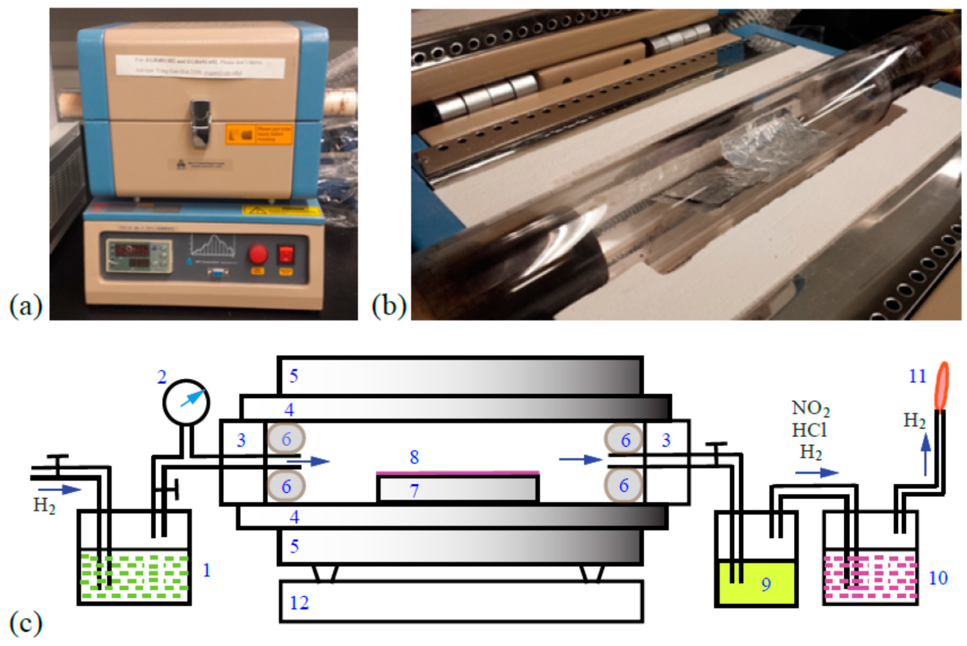
The anodic aluminum oxide (AAO) template used in the experiment was purchased from Whatman Inc. (Piscataway, NJ, USA), and has a pore size of 0.2 μm and a diameter of 25 mm. Nickel acetate, bismuth acetate, iron (III) nitrate, tellurium (IV) chloride, and N,N-dimethylformamide (DMF) were purchased from Alfa Aesar. The precursor solution was made by dissolving nickel acetate, bismuth acetate, copper (II) nitrate, and tellurium (IV) chloride into N,N-dimethylformamide (DMF) in a 250 mL bottle. The nominal concentrations of nickel acetate, copper (II) nitrate, bismuth acetate, and tellurium (IV) chloride were 1.0 M, 0.50 M, 0.1 M, and 0.05 M, respectively. The solution was maintained at a constant temperature of 90 °C. Figure 1 shows the split furnace and CVD chamber used in the experiment as well as a schematic of the overall process. During the CVD, hydrogen was inducted into the solution to carry the volatiles into the quartz reaction chamber which houses the AAO ceramic template for film deposition. The size of the template substrate was 0.5 mm in thickness and 12.5 mm in diameter. The AAO was pre-coated with Au 4 nm thick using a model GSL-1100X-SPC12-LD mini plasma sputtering coater purchased from MTI Corporation, Richmond, CA, USA. The quartz tube was initially vacuumed at a pressure level of 10−2 Torr. During the deposition process, the check valve was open to supply hydrogen at a volumetric flow rate of 5 standard cubic centimeters per minute (sccm) in order to maintain a reducing environment. The furnace was heated up to 500 °C at a ramp rate of 5 °C/min using an MTI GSL-1100X-S50 split furnace (MTI Corporation, Richmond, CA, USA). It was held at 500 °C for 2 h. During the reaction, the exhaust gas was inducted into a container filled with icy water, which allowed the DMF vapor to condense. The by-products from the CVD reactions such as hydrogen chloride and nitrogen oxide were trapped in another container and neutralized by a sodium hydroxide solution with a concentration of 2.0 M. Any remaining hydrogen was burned in a torch. After the experiment, the system was shut down and the specimen was cooled down naturally.

Figure 1.
The chemical vapor deposition set-up and the schematic of the chemical vapor deposition (CVD) process: (a) split furnace; (b) reaction chamber; (c) illustration of the chemical vapor deposition process. 1: precursor solution; 2: vacuum pump; 3: sealing flanges; 4: ceramic tube; 5: heating unit; 6: ceramic foam insulating block; 7: anodic aluminum oxide (AAO) substrate; 8: Bi-Te-Ni-Cu-Au coating; 9: cold trap; 10: sodium hydroxide solution; 11: gas torch; and 12: control unit.
The microstructure of the CVD coating was characterized using a scanning electron microscope (SEM, JEOL JSM-6010PLUS/LA, Peabody, MA, USA). Secondary electron images (SEIs) and the backscattered electron composition (BES) images were taken. The SEIs were compared with the BES image to examine the composition distribution. Quantitative analysis of elements was carried out using energy dispersive X-ray spectroscopy (EDS, equipped with Silicon Drift Detector (SDD)—Model: X-MaxN, made by Oxford Instruments America, Inc., Concord, MA, USA).
The Seebeck coefficient measurement was performed using a self-built facility. In brief, it consisted of two functional units. One was the hot and cold temperature control unit. This unit was built based on two major components, an aluminum heating ring and a digital temperature controller, both purchased from Columbia International Technical Equipment & Supplies LLC, Irmo, SC, USA. The other unit was for open circuit voltage measurement. The voltage measurement unit was made of a model CHI440C Electrochemical Workstation (CH Instrument, Austin, TX, USA). The accessories were from CH Instrument Inc., Austin, TX, USA. During the measurement process, one end of both the nanostructure specimens and the bulk material (in the form of a thick coating) was attached to the aluminum heating ring. The other end of the specimens was exposed to the ambient temperature. The heating ring generated different temperature levels at the hot end of the specimens. The value of the Seebeck coefficient was calculated by the ratio of the voltage to the temperature difference between the hot end and the cold end of the specimens.
To examine the effect of composition, especially the Cu and Au elements on the thermoelectric property (the Seebeck coefficient), comparative studies were conducted by depositing Bi-Te-Ni-Fe film on insulating ceramic substrate. The same MOCVD conditions as described above were used. The chemicals used and the process control for the Bi-Te-Ni-Fe deposition can be found in earlier work [30].
3. Results and Discussion
3.1. Morphology and Composition of the Nanostructure
The microstructure of the anodic aluminum oxide was characterized by various imaging and surface analyses. Figure 2a shows a SEI of the nanoporous AAO. As can be seen, the pore size was around 200 nm. The wall thickness between the pores was also around 200 nm. The energy dispersive X-ray diffraction spectrum in Figure 2b revealed that Al and O were the major elements.
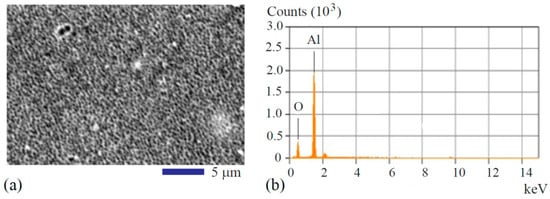
Figure 2.
SEM image of AAO and composition profile: (a) secondary electron image (SEI) of the AAO; (b) energy dispersive X-ray spectroscopy (EDS) showing the qualitative results of Al and O elements.
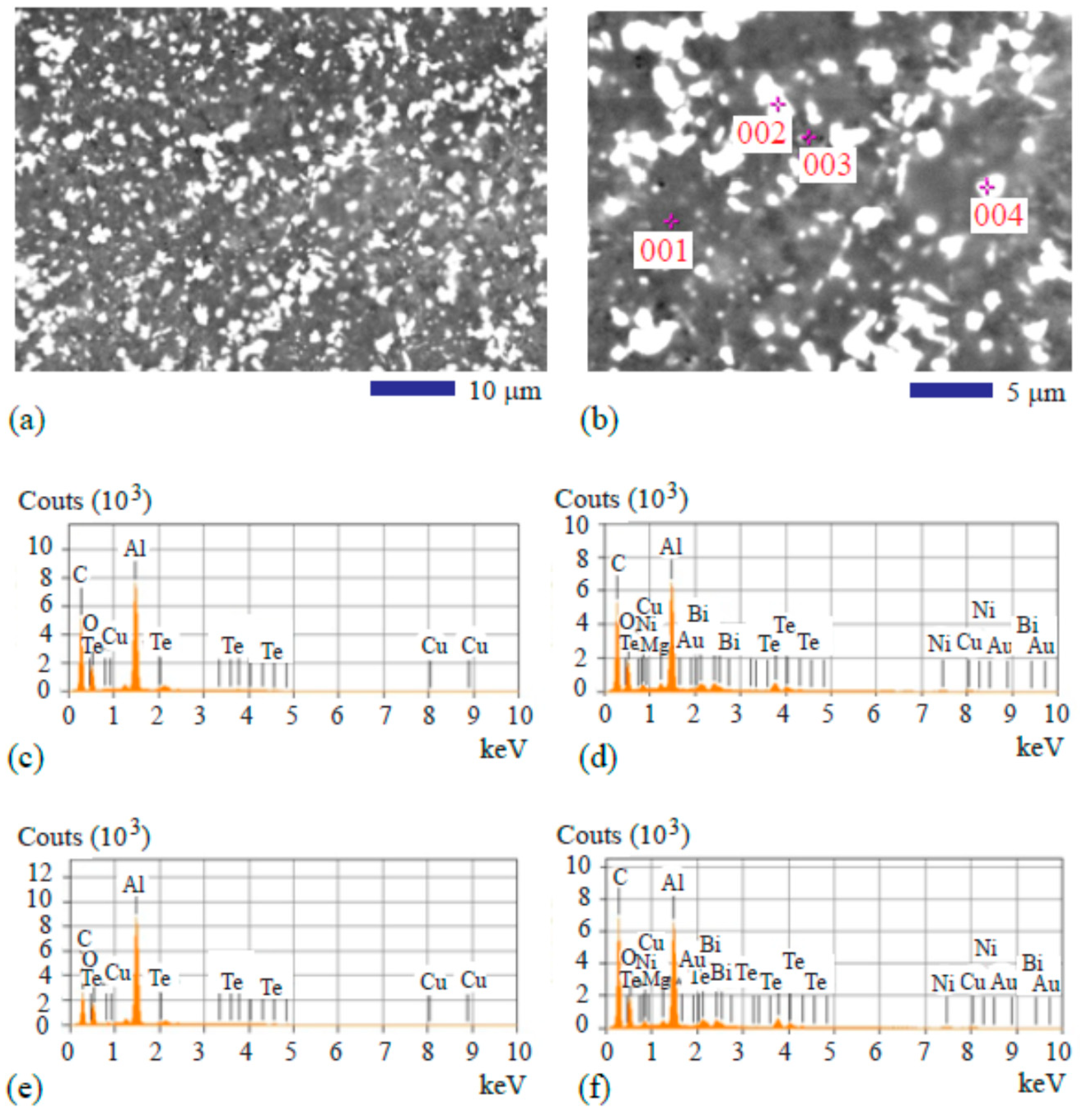
SEM analysis results of the microstructure and the composition of the deposited material are presented in Figure 3. A backscattered electron image for the deposited material is presented in Figure 3a where relatively heavy elements in the coating such as Te and Bi are shown in bright color. The light elements are shown in darker color. Several morphological features including pores, islands and clusters can be easily seen in Figure 3a, which implies a fast growing mechanism of the complex thermoelectric material. Figure 3b shows the locations for spot analysis. Four representative locations were selected.
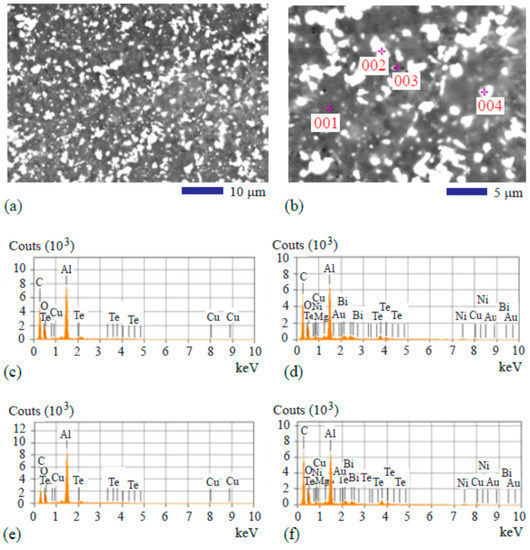
Figure 3.
Spot analysis results: (a) backscattered electron composition (BES) image of the deposited material on AAO; (b) BES image showing the locations for the EDS spot analysis; (c) EDS spectrum for Spot 001; (d) EDS for Spot 002; (e) EDS for Spot 003; (f) EDS for Spot 004.
The qualitative results obtained from the four sites are presented in Figure 3c–f. The compositions in mass percentage for each element from the four spots are presented in Table 1. The spectra in all the four sub-figures illustrate the peaks from five common elements: C, O, Al, Cu, and Te. A carbon signal came from all four spots, indicating that carbon remained from the decomposition of DMF. The oxygen signal could have come from the template, AAO, and decomposition of the DMF.

Table 1.
Mass percentage of elements at the four spots.
At Spot 001, the highest peak of Al was observed because it was the major element from the AAO template; C was the second highest peak. They were followed by the O signal, indicating that the dark shaded region was rich in AAO. At Spot 002, Al still showed the highest peak, while Au, Bi, and Ni were observed. Evidently, Au nanoparticles facilitated the formation of the complex Bi-Te-Al-Ni-Cu material. In addition, some Mg impurity signal was revealed at spot site 002. At Spot 003, C, Al, and O appeared as the major elements, implying that the thermoelectric material had a very low growth rate in this region, which is similar to the observation at Spot 001.
To further validate the catalysis effect of the gold particle, Spot 004 with the similar morphological feature to that at Spot 002 was analyzed. Not surprisingly, Al element still showed the highest peak. Au, Bi, and Ni were also found. This indicates that Au nanoparticles facilitated the formation of the complex Bi-Te-Al-Ni-Cu material. Again, a very small amount of Mg as impurity was found at the location marked as Spot 004. It is well known that gold nanoparticles can be used as the seeds for the formation of nanostructures (e.g., growth of nanoporous Si via solution method and SiGe nanowires via VLS (vapor-liquid-solid) method). Therefore, the Au signal from the EDS analysis is expected to appear only at the sites of the nanostructures (Spots 002 and 004). In the MOCVD process, the Au film de-wets from the alumina surface to form particles and serves as the seeds for the Bi-Te-Ni-Cu growth. The experimental results from the EDS analysis exactly clarify the catalytic function of the gold because only at the sites of the nanostructures (Spots 002 and 004) were the Au peaks found, which is shown by the results in Figure 3d,f.
Quantitative results of mass percentages are listed in Table 1. For Spots 002 and 004, the data in the last two columns yield a relative atomic ratio of Bi to Te of about 2:3. This means that the deposited material was close to the stoichiometry of Bi2Te3 as made by physical vapor deposition reported in [31]. At some other locations, the Bi concentration could be very low. Such behavior was due to the low melting temperature of Bi. Bismuth evaporates faster than telluride does at temperatures above 250 °C, which could result in a Bi to Te ratio less than 2:3.
3.2. Nanostructure Growth Mechanism
Earlier work has proven that gold thin films on polymer substrates possess the tendency to self-assemble into nanoscale dot or particle patterns at elevated temperatures [32]. In this work, a similar temperature effect should exist for the thin gold coating, leading to the formation of gold nanoparticles on the top surface of the AAO. The gold nanoparticles have a high surface area and also a high activity, so they can become active centers for the growth of the complex thermoelectric coating material.
The mechanism of gold nanoparticle assisted catalytic growth is schematically shown in Figure 4. Figure 4a shows the porous AAO. Figure 4b shows the gold coating on it. When the coated AAO was set in the reaction chamber and heated up, the coating shrank due to thermal mechanical effects to form particles, as shown in Figure 4c. The gold nanoparticles then became the centers for the thermoelectric material growth, as illustrated in Figure 4d. As the processing time proceeded, more thermoelectric material was deposited at the interface, as presented in Figure 4e. Eventually, homogenization of the material occurred and the composition of the material became uniform through diffusion, as illustrated in Figure 4f.
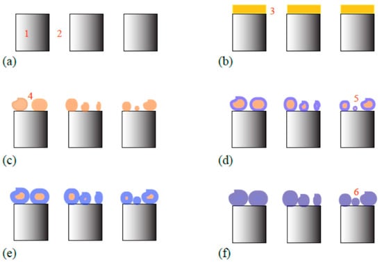
Figure 4.
Schematic showing the gold catalyst assisted chemical vapor deposition mechanism: (a) porous AAO; (b) AAO coated with Au layer; (c) self-assembling of Au layer into nanoparticles at elevated temperatures; (d) Bi-Te-Ni-Cu growth around Au; (e) reaction of Bi-Te-Ni-Cu with Au to form alloy; and (f) homogenization of the complex material to form island like feature. 1: AAO wall, 2: AAO pore, 3: gold layer, 4: gold nanoparticles, 5: interface layer of Bi-Te-Ni-Cu and Au, 6: fully homogenized Bi-Te-Ni-Cu-Au coating.
Gold nanoparticles as the seeds for the formation of nanostructures should keep separation with the growing structures. For example, during the gold nanoparticle catalyst-assisted etching of Si for nanopore array formation, the gold nanoparticles are located at the bottom of the nanopores. In SiGe nanoscale pillar array growth via gold catalyst assisted VLS approach, the gold nanoparticles are always located on the top of the nanowires. Here, we found that gold was eventually merged into the Bi-Te alloy based coating. This is because the Bi-Te has a fairly open and easy exfoliating structure, which allows the gold to be intercalated into the layered structure of the Bi-Te compound.
3.3. Thermoelectric Responses of the Nanostructure vs. Bulk Material (Thick Film)
First, the Seebeck coefficient results of bulk Bi-Te-Ni-Cu-Au thick film material with a coating thickness of 200 nm are presented. The composition of the thick film was the same as for the nanostructure; however, the deposition time was longer to form a thick and continuous film. The hot-end and the cold-end temperature differences were controlled at six values, i.e., 5 °C, 6 °C, 7 °C, 8 °C, 10 °C and 15 °C. For each ΔT, 4000 data were recorded at the rate of 10 data/s. Then the value of Seebeck coefficient, S, was calculated by using the following equation:
The mean and standard deviation of the Seebeck coefficient under each ΔT is listed in Table 2. The final result was obtained as the average of values under different conditions, or Savg = 105.85 ± 10.88 µV/K. This result is comparable to or slightly higher than the currently reported Seebeck coefficient value for Bi-Te bulk material [33] or its composite material [34].
Table 2.
Seebeck coefficient of Bi-Te-Ni-Cu-Au thick film measured at various hot-cold end temperature differences.
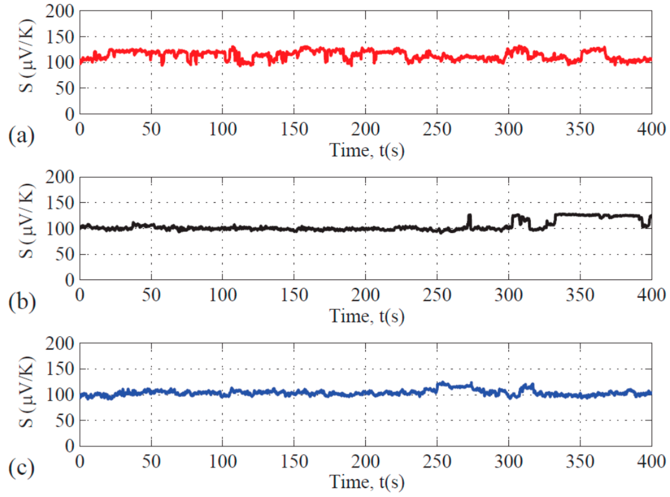
Figure 5 shows three typical curves for the Seebeck coefficient measurement results. These curves provide the information of time-dependent thermoelectric responses of the thick coating at three different values of ΔT: 15 °C, 10 °C and 8 °C. All the plots reveal the relatively stable thermoelectric response of the bulk material.
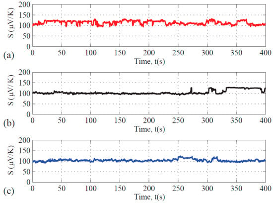
Figure 5.
Seebeck coefficient measurement results of the thick coating obtained from various hot-end to cold-end temperature difference conditions: (a) with ΔT = 15 °C; (b) with ΔT = 10 °C; (c) with ΔT = 8 °C.
The results of the Seebeck effect tests on the nanostructure are summarized in Table 3. All the seven tests consistently delivered a Seebeck coefficient value greater than 200 µV/K. The average value, Savg = 237 ± 13 µV/K, is more than twice the value obtained from the thick film with the same composition.
Table 3.
Seebeck coefficient of the Bi-Te-Ni-Cu-Au nanostructure.
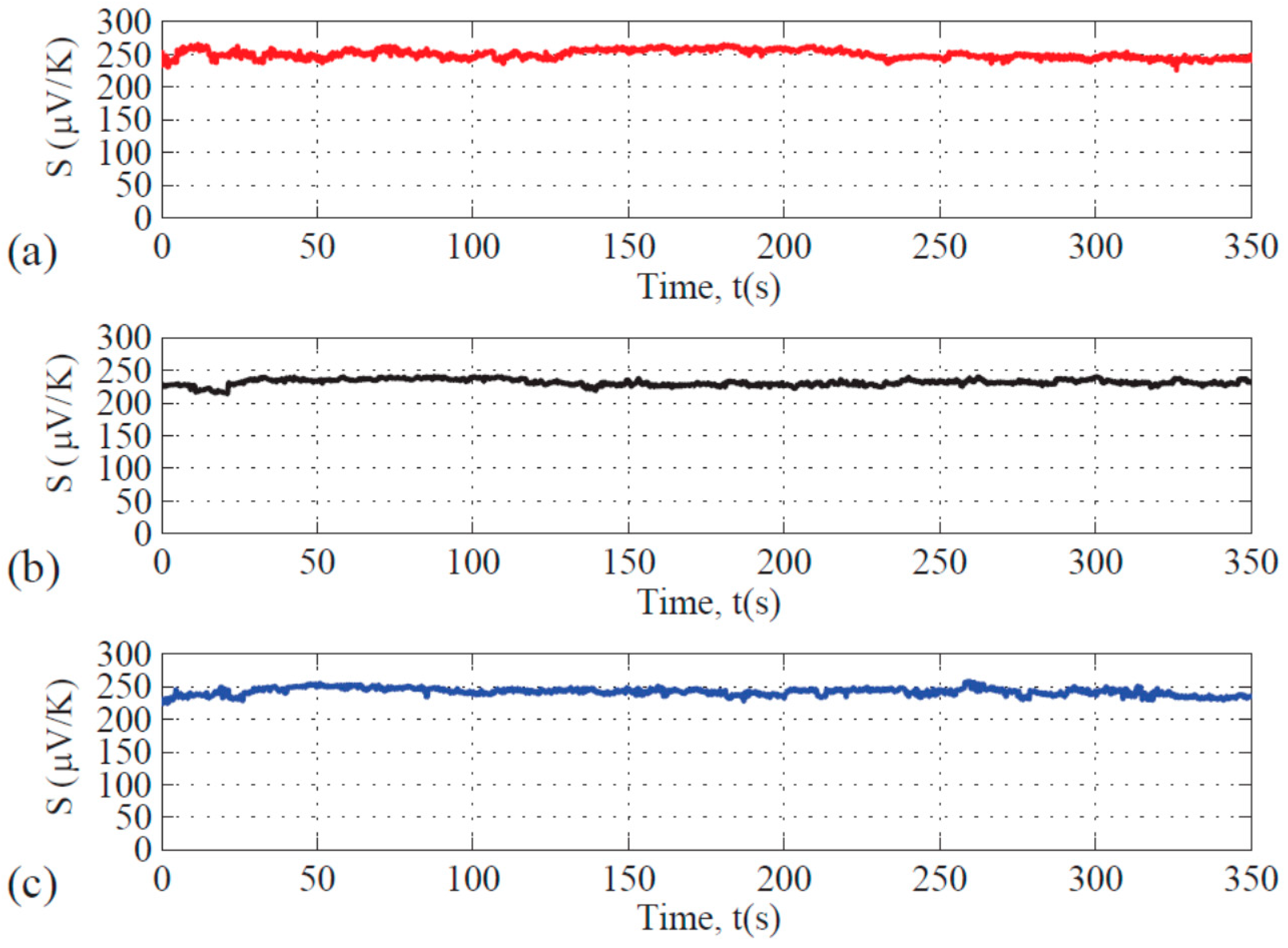
Figure 6 shows results of three specimens of the same nanostructured material at a fixed ΔT of 5 °C. These plots indicate that the thermoelectric response of the nanostructured material is repeatable and that the Seebeck coefficient stayed consistently in the range of 230 and 260 µV/K.
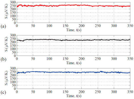
Figure 6.
Time-dependent Seebeck coefficient results of the nanostructure obtained at ΔT = 5 °C to show the reproducible behavior of the nanostructure: (a) from specimen 1, (b) from specimen 2, (c) from specimen 3.
The increase in the Seebeck coefficient of the nanostructured Bi-Te-Ni-Cu-Au thin film is similar to the case for Bi-Te nanoparticles sitting on the silicon nanofibers as shown in [35]. The enhanced Seebeck effect phenomenon can be explained by quantum confinement in the Bi-Te nanostructure. For such a low dimensional nanostructure, the Seebeck coefficient is estimated by the Culter-Mott formula [36]. Although this formula was initially developed for degenerated semiconductors, it may also be applicable for low dimensional structures as mentioned here for a preliminary evaluation. The Seebeck coefficient of the nanostructured Bi-Te-Ni-Cu-Au alloy, S, can be calculated based on the formula containing the Boltzmann constant, the electrical conductivity, the absolute value of the electron charge, the density of charge carriers, the scattering time, and the Fermi energy. The nanostructured particle/thin film materials as prepared in this work were in the one-dimensional (1D) and two-dimensional (2D) form (islands and thin film in a rough AAO plane). The carrier concentration per unit area can be estimated from the effective mass of the charge carriers, their energy levels, and the diameter of the nanoparticles or the thickness of thin film. It is predicted that the Seebeck coefficient should be improved by increasing the electrical conductivity and the scattering time. The finer the nanostructure, or the thinner the film, the higher is the absolute value of the Seebeck coefficient. Therefore, it is reasonable to see that the Bi-Te-Ni-Cu-Au nanostructure demonstrates a stronger Seebeck effect than did the bulk material. The Bi-Te-Ni-Cu-Au nanoscale islands are separated from each other on the surface of the AAO template, leading to reduced electron mobility. This is the mechanism for the enhancement of the Seebeck effect.
The porosity could be a key factor determining both electrical and thermal conductivity of a material. Based on the study of a ZrN material, Adachi et al. [37] found that the thermal conductivity of the porous ZrN, κ, can be calculated by
where κ0 is the bulk conductivity, p the porosity, and β the constant number determined by the conditions of the pores. For spherical pores, β takes a value between 1 and 3 [38].
Obviously, the higher the porosity, the lower the thermal conductivity of the material. Since the thermoelectric figure of merit, zT, is inversely proportional to the thermal conductivity, the reduction in the κ value should be favorable for increasing the thermoelectric energy conversion efficiency. That is the rationale for making the porous film by MOCVD in this work. The implication of the research results in this work is that an inexpensive sensor may be built based on the highly sensitive thermoelectric responses of the Bi-Te-Ni-Cu-Au thin film nanomaterial.
3.4. Composition and Structure Effects on the Thermoelectric Responses
A comparison of Seebeck coefficients of thermoelectric materials with different additives and structures is shown in Table 4. It appears that adding carbon or organic semiconductor into the Bi-Te compound does not significantly increase the Seebeck coefficient of the material [39]. The Bi-Te polyaniline composite has a lowest Seebeck coefficient value of 31 µV/K [40]. The Bi/Bi-Te nanocomposite as shown in [41] demonstrates a Seebeck coefficient value of 185 µV/K, similar to that of the Bi-Te-Ni-Fe thin film, 179 µV/K. The Seebeck coefficient of Bi-Te-Ni-Cu-Au alloy prepared in this work, 237 µV/K, is slightly higher.
Table 4.
Comparison on the absolute value of Seebeck coefficient, S.
The work performed by Tan et al. showed that nanostructured Bi-Te thin film made by radio frequency magnetron sputtering could demonstrate an even higher Seebeck coefficient of 287 µV/K [42]. This again indicates that the charge mobility confinement in nanostructure improves the thermopower of the material. Regarding the role of the copper element, a recent study [43] revealed that it significantly enhances the electrical conductivity of Bi-Te due to carrier concentration. The Bi-Te bulk specimens prepared by the melting method have a smaller Seebeck coefficient. Based on this, the MOCVD Bi-Te-Ni-Cu-Au specimen in porous film form is expected to improve the electrical conductive behavior because the addition of Cu and Au overcomes the decrease in the thermopower of the material.
4. Conclusions
A Bi-Te-Ni-Cu-Au material has been successfully processed by a one-pot precursor approach. Nickel acetate, bismuth acetate, copper (II) nitrate, and tellurium (IV) chloride in N,N-dimethylformamide (DMF) were used as the metal sources for Ni, Bi, Cu, and Te. Hydrogen was used as the carrier gas to prevent oxidation of the Bi-Te-Ni-Cu-Au complex thermoelectric material. The microstructure of the deposited material showed pores and island-like features. The islands were shown in the initial stage of the deposition and such features were due to the existence of noble metal (Au) nanoparticles. The potential applications of the deposited material, including thermoelectric energy conversion and temperature sensing, were validated by the Seebeck coefficient measurements. The nanostructure showed a much greater value of the Seebeck coefficient than did the thick film and bulky material with a similar composition. The reason is the quantum confinement of the nanostructure.
Author Contributions
Y.X.G., M.L. and Z.Y. conceived and designed the experiments; J.B.G., W.C. and Y.X.G. performed the experiments; Y.X.G. and Z.Y. analyzed the data; Y.X.G., Z.Y. and M.L. wrote the paper.
Funding
This work was supported by National Science Foundation (NSF) under Grant Number CMMI-1333044. The SEM images were made possible by the support from National Science Foundation under Grant Number DMR-1429674.
Acknowledgments
Anan S. Hamdan is appreciated for his help on SEM experiments. We also acknowledge the support of the 2017–2018 Provost Teacher-Scholar Program and the 2016–2017 RSCA award from California State Polytechnic University Pomona.
Conflicts of Interest
The authors declare no conflict of interest. The funding sponsors had no role in the design of the study; in the collection, analyses, or interpretation of data; in the writing of the manuscript, and in the decision to publish the results.
References
- Huang, G.; Jian, J.; Lei, R.; Cao, B. Single-crystalline Bi2Se3 nanowires grown by catalyst-free ambient pressure chemical vapor deposition. Mater. Lett. 2016, 179, 198–201. [Google Scholar] [CrossRef]
- Tynell, T.; Aizawa, T.; Ohkubo, I.; Nakamura, K.; Mori, T. Deposition of thermoelectric strontium hexaboride thin films by a low pressure CVD method. J. Cryst. Growth 2016, 449, 10–14. [Google Scholar] [CrossRef]
- Chen, P.; Wang, J.; Lu, Y.; Zhang, S.; Liu, X.; Hou, W.; Wang, Z.; Wang, L. The fabrication of ReS2 flowers at controlled locations by chemical vapor deposition. Phys. E Low-Dimens. Syst. Nanostruct. 2017, 89, 115–118. [Google Scholar] [CrossRef]
- Haase, A.; Peters, A.; Rosiwal, S. Growth and thermoelectric properties of nitrogen-doped diamond/graphite. Diam. Relat. Mater. 2016, 63, 222–226. [Google Scholar] [CrossRef]
- Dávila, D.; Tarancón, A.; Calaza, C.; Salleras, M.; Fernández-Regúlez, M.; San Paulo, A.; Fonseca, L. Improved thermal behavior of multiple linked arrays of silicon nanowires integrated into planar thermoelectric microgenerators. J. Electron. Mater. 2013, 42, 1918–1925. [Google Scholar] [CrossRef]
- Wu, Y.; Fan, R.; Yang, P. Block-by-block growth of single-crystalline Si/SiGe superlattice nanowires. Nano Lett. 2002, 2, 83–86. [Google Scholar] [CrossRef]
- Kim, J.G.; Choi, Y.Y.; Choi, D.J.; Choi, S.M. Study on the thermoelectric properties of CVD SiC deposited with inert gases. J. Electron. Mater. 2011, 40, 840–844. [Google Scholar] [CrossRef]
- Kim, J.G.; Choi, Y.Y.; Choi, D.J.; Kim, J.I.; Kim, B.S.; Choi, S.M. A study on the thermoelectric properties of chemical vapor deposited SiC films with temperature and diluent gases variation. J. Ceram. Soc. Jpn. 2009, 117, 574–577. [Google Scholar] [CrossRef]
- Ngamou, P.H.T.; Bahlawane, N. Chemical vapor deposition and electric characterization of perovskite oxides LaMO3 (M = Co, Fe, Cr and Mn) thin films. J. Solid State Chem. 2009, 182, 849–854. [Google Scholar] [CrossRef]
- Cho, H.S.; Kamins, T.I. In situ control of Au-catalyzed chemical vapor deposited (CVD) Ge nanocone morphology by growth temperature variation. J. Cryst. Growth 2010, 312, 2494–2497. [Google Scholar] [CrossRef]
- Grigorian, L.; Fang, S.; Sumanasekera, G.; Rao, A.M.; Schrader, L.; Eklund, P.C. Physical properties of CVD-grown Se—Carbon films. Synth. Met. 1997, 87, 211–217. [Google Scholar] [CrossRef]
- Giani, A.; Boulouz, A.; Pascal-Delannoy, F.; Foucaran, A.; Boyer, A. MOCVD growth of Bi2Te3 layers using diethyltellurium as a precursor. Thin Solid Films 1998, 315, 99–103. [Google Scholar] [CrossRef]
- Giani, A.; Boulouz, A.; Pascal-Delannoy, F.; Foucaran, A.; Boyer, A. Growth of Bi2Te3 and Sb2Te3 thin films by MOCVD. Mater. Sci. Eng. B 1999, 64, 19–24. [Google Scholar] [CrossRef]
- Venkatasubramanian, R.; Colpitts, T.; Watko, E.; Lamvik, M.; EI-Masry, N. MOCVD of Bi2Te3, Sb2Te3 and their superlattice structures for thin-film thermoelectric applications. J. Cryst. Growth 1997, 170, 817–821. [Google Scholar] [CrossRef]
- Shoko, E. Novel K rattling: A new route to thermoelectric materials? J. Appl. Phys. 2014, 115, 33703–33708. [Google Scholar] [CrossRef]
- Talapin, D.V. Thermoelectric tin selenide: The beauty of simplicity. Angew. Chem. 2014, 53, 9126–9127. [Google Scholar]
- Reddy, P. Electrostatic control of thermoelectricity in molecular junctions. Nat. Nanotechnol. 2014, 9, 881–885. [Google Scholar]
- Xiao, F.; Hangarter, C.; Yoo, B.; Rheem, Y.; Lee, K.H.; Myung, N.V. Recent progress in electrodeposition of thermoelectric thin films and nanostructures. Electrochim. Acta 2008, 53, 8103–8117. [Google Scholar] [CrossRef]
- Tritt, T.M.; Böttner, H.; Chen, L. Thermoelectrics: Direct solar thermal energy conversion. MRS Bull. 2008, 33, 366–368. [Google Scholar] [CrossRef]
- Venkatasubramanian, R.; Siivola, E.; Colpitts, T.; O′Quinn, B. Thin-film thermoelectric devices with high room-temperature figures of merit. Nature 2001, 413, 597–602. [Google Scholar] [CrossRef] [PubMed]
- Majumdar, A. Thermoelectricity in semiconductor nanostructures. Science 2004, 303, 777–778. [Google Scholar] [CrossRef] [PubMed]
- Snyder, G.J.; Toberer, E.S. Complex thermoelectric materials. Nat. Mater. 2008, 7, 105–114. [Google Scholar] [CrossRef] [PubMed]
- Vineis, C.J.; Shakouri, A.; Majumdar, A.; Kanatzidis, M.G. Nanostructured thermoelectrics: Big efficiency gains from small features. Adv. Mater. 2010, 22, 3970–3980. [Google Scholar] [CrossRef] [PubMed]
- He, J.; Tritt, T.M. Advances in thermoelectric materials research: Looking back and moving forward. Science 2017, 357, eaak9997. [Google Scholar] [CrossRef] [PubMed]
- Eklund, P.; Kerdsongpanya, S.; Alling, B. Transition-metal-nitride-based thin films as novel energy harvesting materials. J. Mater. Chem. C 2016, 4, 3905–3914. [Google Scholar] [CrossRef] [PubMed]
- Sun, J.; Li, X.; Guo, W.; Zhao, M.; Fan, X.; Dong, Y.; Xu, C.; Deng, J.; Fu, Y. Synthesis methods of two-dimensional MoS2: A brief review. Crystal 2017, 7, 198. [Google Scholar] [CrossRef]
- Goldsmid, H.J.; Sheard, A.R.; Wright, D.A. The performance of bismuth telluride thermojunctions. Br. J. Appl. Phys. 1958, 9, 365. [Google Scholar] [CrossRef]
- Wang, Z.L.; Onda, T.; Chen, Z.C. Effect of Cu doping on microstructure and thermoelectric properties of Bi2Te2.85Se0.15 bulk materials. Script. Mater. 2018, 146, 119–122. [Google Scholar] [CrossRef]
- Kassu, A.; Farley, C., III; Sharma, A.; Kim, W.; Guo, J. Effect of pore size and film thickness on gold-coated nanoporous anodic aluminum oxide substrates for surface-enhanced Raman scattering sensor. Sensors 2015, 15, 29924–29937. [Google Scholar] [CrossRef] [PubMed]
- Gan, Y.X.; Hamdan, A.S.; Gan, J.B.; Li, M. Chemical vapor deposition of Bi-Te-Ni-Fe on magnesium oxide substrate and its Seebeck effect. Coatings 2017, 7, 164. [Google Scholar] [CrossRef]
- Zhang, G.; Yu, Q.; Wang, W.; Li, X. Nanostructures for thermoelectric applications: Synthesis, growth mechanism, and property studies. Adv. Mater. 2010, 22, 1959–1962. [Google Scholar] [CrossRef] [PubMed]
- Do, M.T.; Tong, Q.C.; Lidiak, A.; Luong, M.H.; Ledoux-Rak, I.; Lai, N.D. Nano-patterning of gold thin film by thermal annealing combined with laser interference techniques. Appl. Phys. A 2016, 122, 360. [Google Scholar] [CrossRef]
- Goldsmid, H.J. Bismuth telluride and its alloys as materials for thermoelectric generation. Materials 2014, 7, 2577–2592. [Google Scholar] [CrossRef] [PubMed]
- Mahmoud, L.; Alhwarai, M.; Samad, Y.A.; Mohammad, B.; Laio, K.; Elnaggar, I. Characterization of a graphene-based thermoelectric generator using a cost-effective fabrication process. Energy Procedia 2015, 75, 615–620. [Google Scholar] [CrossRef]
- Gan, Y.X.; Koludrovich, M.J.; Zhang, L. Thermoelectric effect of silicon nanofibers capped with Bi-Te nanoparticles. Mater. Lett. 2013, 111, 126–129. [Google Scholar] [CrossRef]
- Mott, N.F. Chapter 3: Heavily doped semiconductors. In Conduction in Non-Crystalline Materials; Clarendon Press: Oxford, UK, 1987; p. 53. [Google Scholar]
- Adachi, J.; Kurosaki, K.; Uno, M.; Yamanaka, S. Effect of porosity on thermal and electrical properties of polycrystalline bulk ZrN prepared by spark plasma sintering. J. Alloys Compd. 2007, 432, 7–10. [Google Scholar] [CrossRef]
- Cao, C.Q.; Zhu, T.J.; Zhao, X.B. Low thermal conductivity and improved figure of merit in fine-grained binary PbTe thermoelectric alloys. J. Phys. D Appl. Phys. 2009, 42, 015406. [Google Scholar] [CrossRef]
- Pang, H.; Piao, Y.Y.; Tan, Y.Q.; Jiang, G.Y.; Wang, J.H.; Li, Z.M. Thermoelectric behavior of segregated conductive polymer composites with hybrid fillers of carbon nanotube and bismuth telluride. Mater. Lett. 2013, 107, 150–153. [Google Scholar] [CrossRef]
- Chatterjee, K.; Suresh, A.; Ganguly, S.; Kargupta, K.; Banerjee, D. Synthesis and characterization of an electro-deposited polyaniline-bismuth telluride nanocomposite—A novel thermoelectric material. Mater. Charact. 2009, 60, 1597–1601. [Google Scholar] [CrossRef]
- Sumithra, S.; Takas, N.J.; Misra, D.K.; Nolting, W.M.; Poudeu, P.F.P.; Stokes, K.L. Enhancement in thermoelectric figure of merit in nanostructured Bi2Te3 with semimetal nanoinclusions. Adv. Energy Mater. 2011, 1, 1141–1147. [Google Scholar] [CrossRef]
- Tan, J.; Kalantar-zadeh, K.; Wlodarski, W.; Bhargava, S.; Akolekar, D.; Holland, A.; Rosengarten, G. Thermoelectric properties of bismuth telluride thin films deposited by radio frequency magnetron sputtering. In Smart Sensors, Actuators, and MEMS II, Proceedings of SPIE—The International Society for Optical Engineering, Seville, Spain, 9–11 May 2005; Cane, C., Chiao, J.-C., Verdu, F.V., Eds.; SPIE: Bellingham, WA, USA, 2005; pp. 711–718. [Google Scholar]
- Jung, W.J.; Kim, I.H. Thermoelectric properties of Cu-doped Bi2−xSbxTe3 prepared by encapsulated melting and hot pressing. Met. Mater. Int. 2018, 24, 415–421. [Google Scholar] [CrossRef]


© 2018 by the authors. Licensee MDPI, Basel, Switzerland. This article is an open access article distributed under the terms and conditions of the Creative Commons Attribution (CC BY) license (http://creativecommons.org/licenses/by/4.0/).