Article

Transparent Amorphous Oxide Semiconductor as Excellent Thermoelectric Materials

1
Department of Materials Science and Engineering, Pusan National University, Busan 46241, Korea
2
Department of Physics, Pusan National University, Busan 46241, Korea
3
Department of Electrochemisty, Korea Institute of Materials Science, Changwon 51508, Korea
4
Korea Research Institute of Standards and Science, Daejeon 34113, Korea
5
Department of Physics Education, Pusan National University, Busan 46241, Korea
*
Authors to whom correspondence should be addressed.
Coatings 2018, 8(12), 462; https://doi.org/10.3390/coatings8120462
Submission received: 6 September 2018 / Revised: 3 December 2018 / Accepted: 12 December 2018 / Published: 13 December 2018

Abstract

:
It is demonstrated that transparent amorphous oxide semiconductors (TAOS) can be excellent thermoelectric (TE) materials, since their thermal conductivity (κ) through a randomly disordered structure is quite low, while their electrical conductivity and carrier mobility (μ) are high, compared to crystalline semiconductors through the first-principles calculations and the various measurements for the amorphous In−Zn−O (a-IZO) thin film. The calculated phonon dispersion in a-IZO shows non-linear phonon instability, which can prevent the transport of phonon. The a-IZO was estimated to have poor κ and high electrical conductivity compared to crystalline In2O3:Sn (c-ITO). These properties show that the TAOS can be an excellent thin-film transparent TE material. It is suggested that the TAOS can be employed to mitigate the heating problem in transparent display devices.

Graphical Abstract

1. Introduction

Only approximately 30% of fossil fuel energy is used; therefore, it is desirable to utilize the huge amounts of waste energy. Thermoelectric (TE) materials that convert heat into electrical power are a promising energy technology [1,2,3,4,5,6,7,8,9,10]. The TE materials can be formed either as thin films [1,2,3,4,5,6,7] or as bulk [9,10,11,12,13] semiconductors. Generally, thin-film TE materials have low energy conversion rates due to their thinness compared to bulkier materials. However, an advantage of a thin-film TE material is that the efficiency can be smartly engineered by controlling the nanostructure and composition. Nanostructured TE thin films are especially useful for mitigating heating problems in highly integrated microelectronic devices by accurately controlling the temperature. Hence, there is a rising interest in thin-film TE devices. These devices have been extensively investigated [7,14,15,16].
From a material point of view, oxide semiconductors have attracted much attention due to their lower toxicities and lower prices compared to Te compounds, which are widely used and studied TE materials [2,3]. In2O3 based and ZnO based oxides have been extensively investigated as the transparent conductive oxide for their high electrical conductivity (~3 × 10⁻⁴ Ω·cm), high transmittance (over 80%), and remarkable thermal stability at high temperature [17,18]. These oxides have been intensively investigated recently, especially for applications in display devices. Display devices containing organic materials encounter stability problems related to heating during operation [19]. Hence, the development of transparent TE devices is crucial. The amorphous oxide semiconductors such as a-In−Ga−Zn−O was shown to have high electrical conductivity (σ) and high carrier mobility (μ) comparable to those of the crystalline oxide semiconductor, because the spatially spread metal ns-orbitals with an isotropic shape directly overlap with their closest neighboring ns-orbitals [20,21]. On the other hand, hydrogenated amorphous silicon (a-Si:H) has low μ because of carrier transport by hopping between localized tail-states [22,23].
Previous studies about TE materials as transparent conductive oxides (TCOs) were focused on correlation between figure of merit (ZT) and carrier concentration or a crystal structure. Figure 1 shows ZT values of our results and previous studies as a function of conductivity [24,25,26,27,28,29,30,31,32,33,34,35,36,37,38,39]. The ZT measured at other temperatures were calculated to 300 K. The previous studies’ ZT values were high at low conductivity and decreased with increasing conductivity while our results show high ZT with high conductivity. These results are due to the trade-off relationship between Seebeck coefficient and carrier density and the carrier density being proportional to conductivity. Therefore, research about high ZT thin film with high electrical conductivity is needed.
In this study, we demonstrate that the transparent amorphous oxide semiconductors (TAOS) can be much better as an excellent TE material in the amorphous state rather than crystalline oxide semiconductors. Since amorphous materials have randomly displaced atomic structures, the thermal conductivity (κ) in amorphous oxide semiconductors is expected to be lower compared to that in the crystalline state, while it maintains low resistivity values. Through first-principles electronic and lattice dynamics calculations and various experimental measurements, it is suggested that the amorphous material can have high μ and low κ. Therefore, we suggest that an a-IZO thin film could be a good candidate for a transparent high-performance TE material. This opens the possibility of its use as a transparent thin-film TE material, which will help mitigate the heating problem in transparent display devices.

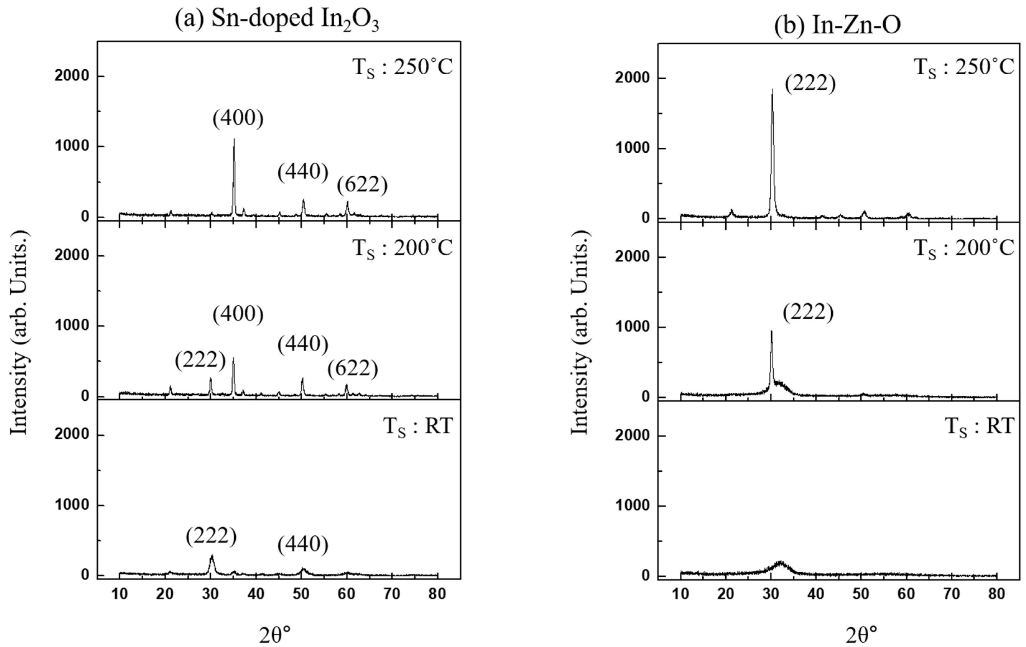
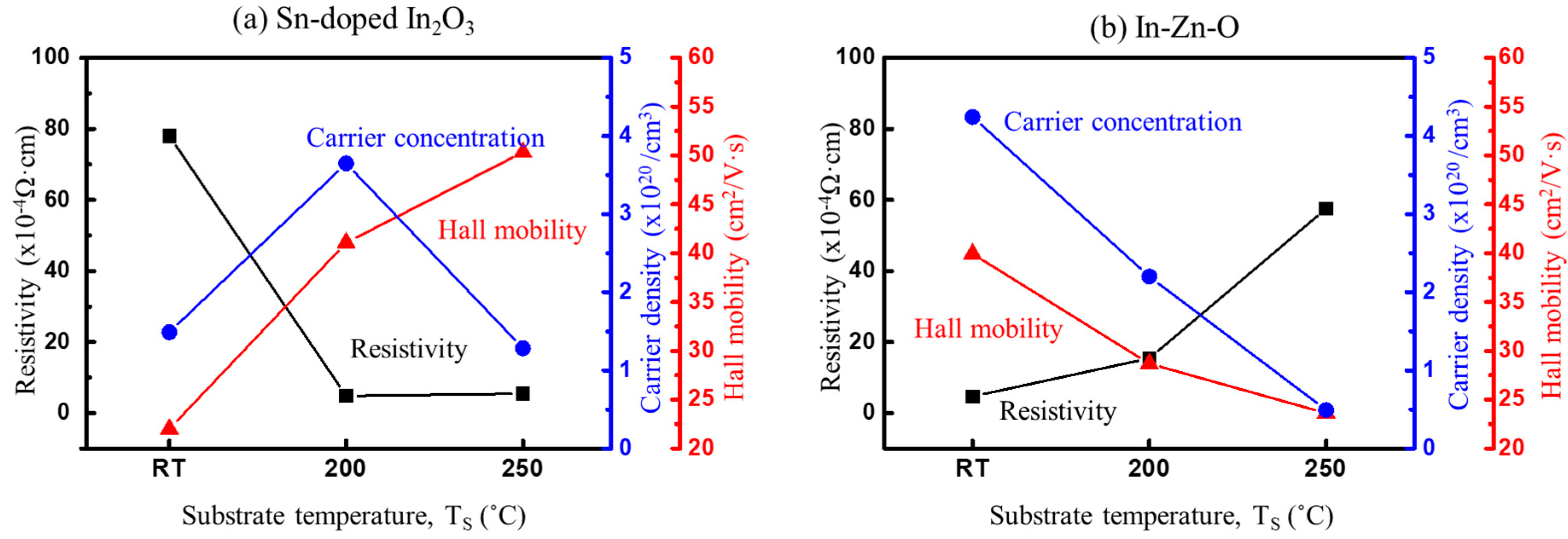
2. Experimental Details

ITO and IZO films with a thickness of 1 ± 0.05 μm were deposited on non-alkali glass by DC magnetron sputtering (DCMS) using ITO (SnO2 10 wt.%) and IZO (ZnO 10 wt.%) single sintered targets. The films were deposited with a DC sputtering power of 70 W (power density: 1.53 W/cm2). The base pressure was exhausted to 1.0 × 10⁻⁵ torr, the total gas pressure was maintained at 5 mtorr using pure Ar gas (5N purity), and the distance between the target and the substrate was 70 mm. The substrate temperature (TS) was varied from room temperature (RT) to 250 °C. The thin-film crystallinity was determined by X-ray diffraction (XRD; Cu kα radiation at 4 keV, 40 mA, θ–2θ mode, BRUKER GADDS, Billerica, MA, USA) analysis. The electrical properties of the thin films were investigated using a Hall effect measurements system (HMS-3000, ECOPIA, Anyang, Korea).
The Seebeck coefficient (S) in the thin films was estimated using a set up Seebeck voltage measurement system. In this measurement system, one side of a sample was maintained at 33 °C, while the temperature of the other side of the sample was maintained at 33, 36, 39 and 42 °C. At this point, the Seebeck voltages were measured. S was calculated from the measured Seebeck voltages and the temperature difference (<3 °C) of the sample ( S = Δ V / Δ T ) .
We estimated the ZT by estimating the value of κ for the thin film. The parameter for evaluating the efficiency of TE materials is the ZT, which is defined as follows:
ZT = S 2 σ T κ e + κ l
where σ is the electrical conductivity, T is the absolute temperature, κe is the electron thermal conductivity, and κl is the phonon thermal conductivity. The power factor (PF) is defined as Equation (2):
PF = S 2 σ
Generally, properties of thin-film TE materials are evaluated by using only PF, because it is hard to measure κ in thin films due to their low thickness compared to the substrate [40]. In his study, ZT was used to evaluate the properties of the TE thin film using the estimated κ value for the thin film. The κ value can be calculated by Equation (3) as follows:
κ = α ρ C p
where κ, α, ρ, and Cp are the total thermal conductivity, thermal diffusivity, density of the thin film, and specific heat of the thin film, respectively. The value of α was measured by the time-domain-thermo-reflectance (TDTR) method, which is a pump-probe optical technique for measuring the thermal properties of materials. The ρ value was measured by using X-ray reflectometry (XRR, EMPYREAN PANalytical, Worcestershire, UK), and a previously reported Cp was used [41]. By using these values, the κ and ZT values were evaluated for the thin films.

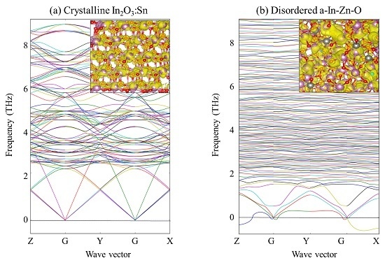
3. First-Principles Atomic Calculations

We performed the first-principles electronic structure calculations to understand the electrical property and the lattice dynamics, which should help to understand the TE properties of amorphous oxides. The calculated values for a-IZO and c-ITO are compared.
First principles calculations were performed with the Vienna ab-initio simulation package (VASP, 5.4.4) [42] using the project augmented wave (PAW) [43] formalism, Perdew–Burke–Ernzerhof (PBE) exchange correlation functional [44] approach, and generalized gradient approximation (GGA). The GGA + U method was used to describe the localized semi-core state of the In-3d and Zn-3d orbitals [45]. We used U = 7 eV for these orbitals, where the semi-core orbitals of Zn-3d is located below the valence band, which describes the microscopic and electronic structure of ZnO better. The U = 7 was applied also to In-d level for consistency to the Zn case.
The atomic structure of c-ITO was simulated by using an In2O3 supercell that consists of 160 atoms, including one Sn donor at an In-site. The atomic structure of a-IZO was generated through an ab-initio molecular dynamics simulation and thermal quenching simulation. In order to generate the metastable amorphous structure, we used a supercell consisting of 150 atoms. We employed the following molecular dynamics processes when performing our calculations. (1) The atoms were randomly located within the supercell, and (2) the melting process was performed at 3500 K with a 1 fs time step; (3) We performed a quenching process. The temperature was slowly lowered to RT, and the atomic structure was fully relaxed through the minimization of atomic forces. In this process, the thermal energy is not fully relaxed; hence, the metastable amorphous structure can be generated; (4) We repeated the above Processes (2) and (3), and the lowest energy structure was chosen. This randomly displaced metastable structure does not fully represent the amorphous structure, but we can gain insight into the physical properties of the amorphous structure.
We calculated the electronic structure of the metastable random structure by using first-principles electronic structure calculations, and phonon dispersion was calculated using the PHONOPY package (1.11.2.80) [46] coupled with the VASP package (5.4.4).
The atomic structure of disordered In−Zn−O simulating an amorphous state and crystalline ITO generated by the molecular dynamics simulation are described in Figure 2. In contrast to c-ITO, the a-IZO structure is severely distorted and the atoms have random locations.
The calculated electronic structure of c-ITO and the generated a-IZO are compared in Figure 3. Remarkably, both the conduction band edges of c-ITO and a-IZO show similar free-electron-like dispersion. Interestingly, even a-IZO shows free-electron-like behavior at the conduction band minimum (CBM). The electron wave function at the CBM is shown in Figure 2d, which is well delocalized, similar to that of c-ITO shown in Figure 2b. On the other hand, the band dispersion of the valence band maximum (VBM) is not free-carrier-like in a-IZO, in contrast to c-ITO. The hole carrier wave function at the VBM in a-IZO is shown in Figure 2c. The hole carrier wave function is strongly localized compared to that of c-ITO. The estimated electron effective mass (me) is 0.206 in ideal In2O3 and 0.209 in crystalline In63SnO96. The value becomes 0.235 for In55Sn9O96, indicating that it becomes larger in the presence of Sn. On the other hand, the me in In63ZnO96 is calculated to be 0.204 in the presence of Zn, which is similar to that for Sn-doped In2O3. However, the value becomes 0.191 for a higher concentration of In55Zn9O96.
For a-In−Zn−O, the estimated me in amorphous In54Zn8O88 is 0.181–0.185 and is nearly independent of the k-direction, which is surprisingly smaller than the value in c-ITO, as expected from the wave function. Since the band width of the conduction band edge in a-IZO is comparable to that in c-ITO, the effect of defects and thermal vibration should be weak, according to the Anderson localization concept, in both a-IZO and c-ITO.
In order to describe the localization characters of the wave functions, we performed the inverse participation ratio analysis of the wave functions of the electronic states. Through the angular momentum decompositions of wave functions and the summation of orbital components belonging to atoms, Ψ i ( E ) = i c i ,   E ϕ i were obtained, where i denotes atom, and φi includes all atomic orbitals of an i-atom. The normalized inverse participation ratio of the atomic mapping of the wave functions was calculated by the Equation (4):
IPR ( E ) = ( 1 N i c i ,   E 4 ) / ( 1 N i c i ,   E 2 ) 2
The IPR = 1 describes that a wave function is equally distributed over all atoms. The larger value of IPR indicates the more serious localization at some atoms. The calculated results of IPR(E) depending on the energy are shown at the right of the band structures in Figure 3. The calculated IPR indicate that the conduction band edges of both c-ITO and a-IZO are similarly well delocalized, and the IPR values are about 1.2 for both c-ITO and a-IZO. These results indicate that a-IZO should have good electrical conductivity and high μ, comparable to those of c-ITO. On the other hand, around the VBM, some localized band tail states develop in the a-IZO, differently from the c-ITO. The IPR value at VBM of a-IZO becomes 29.3. Furthermore, the band dispersion at the VBM of a-IZO is nearly flat. Thus, it is expected that the hole carrier mobility is low in a-IZO.
Figure 4 shows the calculated phonon dispersion relations in c-ITO and a-IZO. It is found that the phonon band in a-IZO is very different from that in c-ITO. The dispersion of the low energy phonon is flatter in a-IZO, which indicates that the phonon velocity should be lower than that in c-ITO. Furthermore, a-IZO shows a negative phonon frequency, indicating some phonon anomaly. It indicates that some phonons should be absorbed and destroyed more easily in the amorphous state compared to the crystalline state. Based those calculated results, we suggest that a-IZO should have good electrical n-type conductivity and poor κ, which are desirable for excellent TE materials. Conventionally, the 2-dimensional structured materials have been investigated to obtain the poor κ. Here it is shown that the poor κ is simply achieved by the amorphous structure.

4. Experimental Measurements and Discussion

ITO and IZO are typical transparent materials, however it is well known that the ITO is easily crystallized, whereas the In−Zn−O formed at low-temperature deposition tends to be amorphous [47,48]. Therefore, we compared the TE properties of these two materials.
Figure 5 shows the XRD patterns of the ITO and IZO thin films deposited at various temperature: RT, 200, and 250 °C. In the ITO films, all films showed the character of crystallized structure, regardless of substrate temperature (TS). The sample deposited at RT shows a prevalent preferred orientation C (222). However, the sample deposited at 200 and 250 °C shows a preferred orientation of (400). The peak intensity increased relative to TS, and the C (400) peak that appears near 2θ = 35° sharply increased. In general, the ITO thin film shows a preferential orientation, as indicated by the C (222) peak. However, in this case, the ITO film shows a C (400) preferential orientation caused by high energy bombardment, which occurs during relatively long deposition times, compared to the ITO thin film with thickness of 150 nm. It is well known that reflected neutral Ar and negative oxygen ions form during sputtering, and these high-energy particles cause the sputtered films to crystallize during deposition [48,49,50,51].
On the other hand, it is shown that the In−Zn−O deposited at RT exhibited the character of amorphous structure [52,53]. The IZO deposited at higher TS was partially crystallized. The samples deposited at 200 and 250 °C show a C (222) peak near 2θ = 30°, which indicates a crystalline structure. It is confirmed that the crystallization temperature of an In−Zn−O film with 1 μm thickness is between RT and 200 °C. It is found that the IZO sample deposited at RT could have a higher ZT value due to a low κ value in the amorphous structure, to be discussed below.
In Figure 6, we compare the resistivity, carrier density (n), and μ of (a) ITO and (b) IZO thin films deposited at RT, 200, and 250 °C. Notably, the resistivity of the ITO film decreased at higher TS values, whereas that of IZO increased. Even if the a-IZO film deposited at RT is in the amorphous state, it shows the lowest resistivity (4.644 × 10⁻⁴ Ω·cm), highest μ, and highest n values. The high n value should be due to non-stoichiometry by oxygen deficiency. As TS increase, both μ and the n decrease, which are understood to be due to improved crystallinity that causes decrease of oxygen vacancy.
The ITO film deposited at a higher temperature clearly showed a higher μ value. However, the n value in the sample grown at 250 °C is lower than that in the sample grown at 200 °C, despite the fact that μ was higher for a higher TS value. The lower n value for TS = 250 °C is due to a decrease of oxygen vacancies that comes from higher crystallinity [33,36,37].
Figure 7 shows a comparison between the S and PF value in the ITO and IZO films deposited at various TS values. In degenerated semiconductors, S is generally defined as follows:
S = 8 π 2 k B 2 3 e h 2 ( π 3 n ) 2 3 m * T
Every film has a negative S value, since these materials are n-type semiconductors. The value of S decreased in the case of ITO films with an increased TS value, whereas it increased in a-IZO.
The highest PF value (310.4 μW K−2 m−1) was observed in ITO deposited at 200 °C, whereas the highest PF value was observed in the a-IZO sample deposited at RT (PF: 354.6 μW K−2 m−1). PF was calculated by Equation (2), and the electrical conductivity was calculated using σ = neμ. In Equation (2) S and the conductivity values show a trade-off with respect to n, since σ ~ n, whereas S ~ 1/n. On the other hand, the electrical conductivity is proportional to µ.
We compared the best TE properties observed in c-ITO (TS = 200 °C) to those in the as-grown a-IZO in Table 1. An important finding is that a-IZO has much better TE properties compared to c-ITO, and a-IZO has a ZT value nearly twice that of c-ITO. Since their electrical conductivities are similar, the difference in TE properties are primarily due to a difference in κ, as expected from the theoretical calculation. The κ value in these materials is the sum of electron thermal conductivity (κe) and phonon thermal conductivity (κl) values. The κe value was estimated using the Equation (6) Wiedemann–Franz law [38]:
κ e = L 0 T / ρ
where L0 is the Lorentz constant. The κl value was estimated by subtracting the κe value from the κ value determined by TDTR. There are no significant differences in κe between c-ITO and a-IZO because they have similar n, although κe in a-IZO is slightly lower than that in c-ITO. This difference arises due to the structural properties. However, κl in c-ITO is much higher than in a-IZO, as expected, since the atomic structure of a-IZO should have random distortions as shown in Figure 2. Accordingly, the κ value in a-IZO is lower than that in c-ITO. In the case of an a-IZO thin film, the ZT value is high due to good electrical conductivity, while the low κ value is due to the amorphous structure.

5. Conclusions

It has been demonstrated through first-principles calculations and various experimental measurements that the transparent amorphous oxide semiconductor (TAOS) can function as an excellent thermoelectric material. It was shown that a-IZO can have high μ and electrical conductivity values, while having a low κ value. The first-principles calculations show that a-IZO has a lattice instability in the randomly distorted structure, which should prevent the phonon transport; meanwhile, the conduction band of a-IZO has a well-delocalized free-electron-like state, indicating that the μ should be comparable to that of crystalline oxide semiconductor. We estimated the electrical and TE properties of a-IZO and c-ITO and confirmed that the ZT values in a-IZO is approximately twice that in c-ITO. These results can be explained by the low κl value in a-IZO, while the PF values in c-ITO and a-IZO are comparable. Based on these results, we suggest that the thin-film TAOS should be an excellent thermoelectric material and can be engaged to resolve the heating problem in transparent display devices.

Author Contributions

Conceptualization, S.K. and P.S.; Data Curation, D.K., J.B., and S.P.; Formal Analysis, J.L.; Investigation, J.S.; Project Administration, S.P.; Supervision, S.K. and P.S.; Writing–Original Draft Preparation, S.K.; Writing–Review & Editing, S.K.

Funding

This work was funded by a National Research Foundation of Korea (NRF) grant funded by the Korea government (MSIP) (No. 2018R1A5A1025594), and partially supported by the National Research Foundation of Korea (NRF) grant (No. 2017R1A2B4012144 and 2015M3D1A1070609).

Conflicts of Interest

The authors declare no conflict of interest.

References

  1. Zhou, Y.; Tan, Q.; Zhu, J.; Li, S.; Liu, C.; Lei, Y.; Li, L. Thermoelectric properties of amorphous Zr–Ni–Sn thin films deposited by magnetron sputtering. J. Electron. Mater. 2015, 44, 1957–1962. [Google Scholar] [CrossRef]
  2. Kim, D.-H.; Byon, E.; Lee, G.H.; Cho, S. Effect of deposition temperature on the structural and thermoelectric properties of bismuth telluride thin films grown by co-sputtering. Thin Solid Films 2006, 510, 148–153. [Google Scholar] [CrossRef]
  3. Yoo, I.-J.; Song, Y.; Lim, D.C.; Myunug, N.V.; Lee, K.H.; Oh, M.; Lee, D.; Kim, Y.D.; Kim, S.; Choa, Y.H.; et al. Thermoelectric characteristics of Sb2Te3 thin films formed via surfactant-assisted electrodeposition. J. Mater. Chem. A 2013, 1, 5430–5435. [Google Scholar] [CrossRef]
  4. Liu, H.; Fang, L.; Wu, F.; Tian, D.; Li, W.; Lu, Y.; Kong, C.; Zhang, S. Thermoelectric and magneto-thermoelectric properties of Ga-doped ZnO thin films by RF magnetron sputtering. Surf. Rev. Lett. 2014, 21, 1450033. [Google Scholar] [CrossRef]
  5. Fang, L.; Yang, X.F.; Peng, L.P.; Zhou, K.; Wu, F.; Huang, Q.L.; Kong, C.Y. Thermoelectric and magnetothermoelectric properties of In-doped nano-ZnO thin films prepared by RF magnetron sputtering. J. Supercond. Nov. Magn. 2010, 23, 889–892. [Google Scholar] [CrossRef]
  6. Sajad, Y.; Pettes, M.T. Nanoscale self-assembly of thermoelectric materials: A review of chemistry-based approaches. Nanotechnology 2018, 29, 432001. [Google Scholar] [CrossRef] [PubMed]
  7. Harman, T.C.; Taylor, P.J.; Walsh, M.P.; LaForge, B.E. Quantum dot superlattice thermoelectric materials and devices. Science 2002, 297, 2229–2232. [Google Scholar] [CrossRef] [PubMed]
  8. Hsu, K.F.; Loo, S.; Guo, F.; Chen, W.; Dyck, J.S.; Uher, C.; Hogan, T.; Polychroniadis, E.K.; Kanatzidis, M.G. Cubic AgPbmSbTe2+m: Bulk thermoelectric materials with high figure of merit. Science 2004, 303, 818–821. [Google Scholar] [CrossRef] [PubMed]
  9. Dughaish, Z.H. Lead telluride as a thermoelectric material for thermoelectric power generation. Phys. B Condens. Matter 2002, 322, 205–223. [Google Scholar] [CrossRef]
  10. Lan, Y.; Minnich, A.J.; Chen, G.; Ren, Z. Enhancement of thermoelectric figure-of-merit by a bulk nanostructuring approach. Adv. Funct. Mater. 2010, 20, 357–376. [Google Scholar] [CrossRef]
  11. Kuo, C.H.; Jeng, M.S.; Ku, J.R.; Wu, S.K.; Chou, Y.W.; Hwang, C.S. p-Type PbTe thermoelectric bulk materials with nanograins fabricated by attrition milling and spark plasma sintering. J. Electron. Mater. 2009, 38, 1956–1961. [Google Scholar] [CrossRef]
  12. Poudel, B.; Hao, Q.; Ma, Y.; Lan, Y.; Minnich, A.; Yu, B.; Yan, X.; Wang, D.; Muto, A.; Vashaee, D.; et al. High-thermoelectric performance of nanostructured bismuth antimony telluride bulk alloys. Science 2008, 320, 634–638. [Google Scholar] [CrossRef] [PubMed]
  13. Wang, H.; Li, J.F.; Nan, C.W.; Zhou, M.; Liu, W.; Zhang, B.P.; Kita, T. High-performance Ag0.8Pb18+xSbTe20 thermoelectric bulk materials fabricated by mechanical alloying and spark plasma sintering. Appl. Phys. Lett. 2006, 88, 092104. [Google Scholar] [CrossRef]
  14. Blackburn, J.L.; Ferguson, A.J.; Cho, C.; Grunlan, J.C. Carbon-nanotube-based thermoelectric materials and devices. Adv. Mater. 2018, 30, 1704386. [Google Scholar] [CrossRef] [PubMed]
  15. Erickson, K.J.; Leonard, F.; Stavila, V.; Foster, M.E.; Spataru, C.D.; Jones, R.E.; Foley, B.M.; Hopkins, P.E.; Allendorf, M.D.; Talin, A.A. Thin film thermoelectric metal–organic framework with high Seebeck coefficient and low thermal conductivity. Adv. Mater. 2015, 27, 3453–3459. [Google Scholar] [CrossRef]
  16. Catellani, A.; Ruini, A.; Nardelli, M.B.; Calzolari, A. Unconventional co-existence of plasmon and thermoelectric activity in In:ZnO nanowires. RSC Adv. 2015, 5, 44865–44872. [Google Scholar] [CrossRef]
  17. Castro, M.V.; Tavares, C.J. Dependence of Ga-doped ZnO thin film properties on different sputtering process parameters: Substrate temperature, sputtering pressure and bias voltage. Thin Solid Films 2015, 586, 13–21. [Google Scholar] [CrossRef] [Green Version]
  18. Granqvist, C.G.; Hultaker, A. Transparent and conducting ITO films: New developments and applications. Thin Solid Films 2002, 411, 1–5. [Google Scholar] [CrossRef]
  19. Park, J.; Lee, J.; Noh, Y.-Y. Optical and thermal properties of large-area OLED lightings with metallic grids. Org. Electron. 2012, 13, 184–194. [Google Scholar] [CrossRef]
  20. Hosono, H. Ionic amorphous oxide semiconductors: Material design, carrier transport, and device application. J. Non-Cryst. Sol. 2006, 352, 851–858. [Google Scholar] [CrossRef]
  21. Nomura, K.; Ohta, H.; Takagi, A.; Kamiya, T.; Hirano, M.; Hosono, H. Room-temperature fabrication of transparent flexible thin-film transistors using amorphous oxide semiconductors. Nature 2004, 432, 488–492. [Google Scholar] [CrossRef]
  22. Carey, P.G.; Smith, P.M.; Theiss, S.D.; Wickboldt, P. Polysilicon thin film transistors fabricated on low temperature plastic substrates. J. Vac. Sci. Technol. A 1999, 17, 1946–1949. [Google Scholar] [CrossRef]
  23. Yang, C.-S.; Smith, L.L.; Arthur, C.B.; Parsons, G.N. Stability of low-temperature amorphous silicon thin film transistors formed on glass and transparent plastic substrates. J. Vac. Sci. Technol. B 2000, 18, 683–689. [Google Scholar] [CrossRef]
  24. Hong, M.-H.; Jung, S.-Y.; Ha, T.-J.; Seo, W.-S.; Lim, Y.S.; Shin, S.; Cho, H.H.; Park, H.-H. Thermoelectric properties of mesoporous TiO2 thin films through annealing temperature and ratio of surfactant. Surf. Coat. Technol. 2013, 231, 370–373. [Google Scholar] [CrossRef]
  25. Aksit, M.; Kolli, S.K.; Slauch, I.M.; Robinson, R.D. Misfit layered Ca3Co4O9 as a high figure of merit p-type transparent conducting oxide film through solution processing. Appl. Phys. Lett. 2014, 104, 161901. [Google Scholar] [CrossRef]
  26. Saini, S.; Mele, P.; Honda, H.; Suzuki, T.; Matsumoto, K.; Miyazaki, K.; Ichinose, A.; Molina Luna, L.; Carlini, R.; Tiwari, A. Effect of self-grown seed layer on thermoelectric properties of ZnO thin films. Thin Solid Films 2016, 605, 289–294. [Google Scholar] [CrossRef] [Green Version]
  27. Jha, P.; Sands, T.D.; Jackson, P.; Bomberger, C.; Favaloro, T.; Hodson, S.; Zide, J.; Xu, X.; Shakouri, A. Cross-plane thermoelectric transport in p-type La0.67Sr0.33MnO3/LaMnO3 oxide metal/semiconductor superlattices. J. Appl. Phys. 2013, 113, 193702. [Google Scholar] [CrossRef]
  28. Ravichandran, J. Thermoelectric and thermal transport properties of complex oxide thin films, heterostructures and superlattices. J. Mater. Res. 2017, 32, 183–203. [Google Scholar] [CrossRef]
  29. Fan, P.; Li, Y.Z.; Zheng, Z.H.; Lin, Q.Y.; Luo, J.T.; Liang, G.X.; Zhang, M.; Chen, M. Thermoelectric properties optimization of Al-doped ZnO thin films prepared by reactive sputtering Zn–Al alloy target. Appl. Surf. Sci. 2013, 284, 145–149. [Google Scholar] [CrossRef]
  30. Mele, P.; Saini, S.; Honda, H.; Matsumoto, K.; Miyazaki, K.; Hagino, H.; Ichinose, A. Effect of substrate on thermoelectric properties of Al-doped ZnO thin films. Appl. Phys. Lett. 2013, 102, 253903. [Google Scholar] [CrossRef]
  31. Saini, S.; Mele, P.; Honda, H.; Matsumoto, K.; Miyazaki, K.; Luna, L.M.; Hopkins, P.E. Influence of postdeposition cooling atmosphere on thermoelectric properties of 2% Al-doped ZnO thin films grown by pulsed laser deposition. J. Electron. Mater. 2015, 44, 1547–1553. [Google Scholar] [CrossRef]
  32. Robert, R.; Aguirre, M.H.; Bocher, L.; Trottmann, M.; Heiroth, S.; Lippert, T.; Döbeli, M.; Weidenkaff, A. Thermoelectric properties of LaCo1−xNixO3 polycrystalline samples and epitaxial thin films. Solid State Sci. 2008, 10, 502–507. [Google Scholar] [CrossRef]
  33. Saini, S.; Mele, P.; Honda, H.; Henry, D.J.; Hopkins, P.E.; Molina-Luna, L.; Matsumoto, K.; Miyazaki, K.; Ichinose, A. Enhanced thermoelectric performance of Al-doped ZnO thin films on amorphous substrate. Jpn. J. Appl. Phys. 2014, 53, 060306. [Google Scholar] [CrossRef]
  34. Vogel-Schäuble, N.; Romanyuk, Y.E.; Yoon, S.; Saji, K.J.; Populoh, S.; Pokrant, S.; Aguirre, M.H.; Weidenkaff, A. Thermoelectric properties of nanostructured Al-substituted ZnO thin films. Thin Solid Films 2012, 520, 6869–6875. [Google Scholar] [CrossRef]
  35. Vogel-Schäuble, N.; Jaeger, T.; Romanyuk, Y.E.; Populoh, S.; Mix, C.; Jakob, G.; Weidenkaff, A. Thermal conductivity of thermoelectric Al-substituted ZnO thin films. Phys. Status Solidi Rapid Res. Lett. 2013, 7, 364–367. [Google Scholar] [CrossRef]
  36. Brinks, P.; Heijmerikx, H.; Hendriks, T.A.; Rijnders, G.; Huijben, M. Achieving chemical stability in thermoelectric NaxCoO2 thin films. RSC Adv. 2012, 2, 6023–6027. [Google Scholar] [CrossRef]
  37. Tran Nguyen, N.H.; Nguyen, T.H.; Liu, Y.; Aminzare, M.; Pham, A.T.T.; Cho, S.; Wong, D.P.; Chen, K.-H.; Seetawan, T.; Pham, N.K.; et al. Thermoelectric properties of indium and gallium dually doped ZnO thin films. ACS Appl. Mater. Interfaces 2016, 8, 33916–33923. [Google Scholar] [CrossRef]
  38. Korotcenkov, G.; Brinzari, V.; Cho, B.K. In2O3-based multicomponent metal oxide films and their prospects for thermoelectric applications. Solid State Sci. 2016, 52, 141–148. [Google Scholar] [CrossRef]
  39. Ono, Y.; Satoh, K.-I.; Nozaki, T.; Kajitani, T. Structural, magnetic and thermoelectric properties of delafossite-type oxide, CuCr1−xMgxO2 (0 ≤ x ≤ 0.05). Jpn. J. Appl. Phys. 2007, 46, 1071. [Google Scholar] [CrossRef]
  40. Seo, D.K.; Shin, S.; Cho, H.H.; Kong, B.H.; Whang, D.M.; Cho, H.K. Drastic improvement of oxide thermoelectric performance using thermal and plasma treatments of the InGaZnO thin films grown by sputtering. Acta Mater. 2011, 59, 6743–6750. [Google Scholar] [CrossRef]
  41. Endoh, R.; Hirano, T.; Takeda, M.; Oishi, M.; Oka, N.; Shigesato, Y. Thermal conductivity of amorphous indium zinc oxide thin films. In Proceedings of the Transparent Conducting Oxides and Applications, Boston, MA, USA, 29 November–3 December 2010. [Google Scholar]
  42. Kresse, G.; Furthmuller, J. Efficient iterative schemes for ab initio total-energy calculations using a plane-wave basis set. Phys. Rev. B 1996, 54, 11169. [Google Scholar] [CrossRef]
  43. Blöchl, P.E. Projector augmented-wave method. Phys. Rev. B 1994, 50, 17953. [Google Scholar] [CrossRef]
  44. Perdew, J.P.; Burke, K.; Ernzerhof, M. Generalized gradient approximation made simple. Phys. Rev. Lett. 1996, 77, 3865. [Google Scholar] [CrossRef]
  45. Anisimov, V.I.; Zaanen, J.; Andersen, O.K. Band theory and Mott insulators: Hubbard U instead of Stoner I. Phys. Rev. B 1991, 44, 943. [Google Scholar] [CrossRef]
  46. Togo, A.; Tanaka, I. First principles phonon calculations in materials science. Scripta Mater. 2015, 108, 1–5. [Google Scholar] [CrossRef] [Green Version]
  47. Byeon, J.; Kim, S.; Lim, J.-H.; Song, J.Y.; Park, S.H.; Song, P. Thermoelectric and electrical properties of micro-quantity Sn-doped amorphous indium-zinc oxide thin films. Jpn. J. Appl. Phys. 2017, 56, 010304. [Google Scholar] [CrossRef]
  48. Song, P.K.; Shigesato, Y.; Kamei, M.; Yasui, I. Electrical and structural properties of tin-doped indium oxide films deposited by DC sputtering at room temperature. Jpn. J. Appl. Phys. 1999, 38, 2921. [Google Scholar] [CrossRef]
  49. Kim, H.; Gilmore, C.M.; Pique, A.; Horwitz, J.S.; Mattoussi, H.; Murata, H.; Kafafi, Z.H.; Chrisey, D.B. Electrical, optical, and structural properties of indium-tin-oxide thin films for organic light-emitting devices. J. Appl. Phys. 1999, 86, 6451–6461. [Google Scholar] [CrossRef]
  50. Kim, H.K.; Kim, D.G.; Lee, K.S.; Huh, M.S.; Jeong, S.H.; Kim, K.I.; Seong, T.Y. Plasma damage-free sputtering of indium tin oxide cathode layers for top-emitting organic light-emitting diodes. Appl. Phys. Lett. 2005, 86, 186503. [Google Scholar] [CrossRef]
  51. Shigesato, Y.; Paine, D.C. A microstructural study of low resistivity tin-doped indium oxide prepared by d.c. magnetron sputtering. Thin Solid Films 1994, 238, 44–50. [Google Scholar] [CrossRef]
  52. Yaglioglu, B.; Yeom, H.-Y.; Paine, D.C. Crystallization of amorphous In2O3–10 wt.% ZnO thin films annealed in air. Appl. Phys. Lett. 2005, 86, 261908. [Google Scholar] [CrossRef]
  53. Garf, M.J.; Yip, S.-K.; Sauls, J.A. Electronic thermal conductivity and the Wiedemann-Franz law for unconventional superconductors. Phys. Rev. B 1996, 53, 15147. [Google Scholar] [CrossRef]
Figure 1. Thermoelectric figure of merit of oxide thin films as a function of conductivity. The ZT measured at other temperature is calculated to 300 K.
Coatings 08 00462 g001
Figure 2. Atomic structure and electron densities of the band edges of polycrystalline In−Sn−O (c-ITO) and disordered amorphous In−Zn−O (a-IZO) generated by molecular dynamics simulation (a) valence band maximum (VBM), (b) conduction band minimum (CBM) of c-ITO, (c) VBM and (d) CBM of a-IZO. Except VBM of a-IZO, all wave-functions are well-delocalized. The pink and red balls represent In and O atoms, respectively, and grey balls represent the Sn atom in (a,b), and Zn in (c,d). The isosurface was selected at 0.0003 e/supercell.
Coatings 08 00462 g002
Figure 3. Electronic structures and IPR of (a) crystalline In55Sn9O96 and (b) disordered amorphous In54Zn8O88 generated by the ab-initio molecular dynamics simulation are compared. (a) was calculated by using an In2O3 supercell containing 160 atoms, where an In atom was replaced by a Sn atom. (b) was calculated using a supercell with 150 atoms.
Coatings 08 00462 g003
Figure 4. Calculated dispersion relations of phonon states by the first-principles calculation are compared between (a) crystalline In55Sn9O96 and (b) disordered amorphous In54Zn8O88 generated by the ab-initio molecular dynamics simulation. Here, Z, Y, X, and G are (0,0,1/2), (0,1/2,0), (1/2,0,0), and (0,0,0) points in the Brillouin zone, respectively.
Coatings 08 00462 g004
Figure 5. XRD patterns of (a) c-ITO and (b) a-IZO films with a thickness of 1 µm deposited under various substrate temperatures (TS: RT, 200, and 250 °C) are compared. The IZO grown at RT shows the amorphous state.
Coatings 08 00462 g005
Figure 6. Resistivity (■), carrier concentration (), and Hall mobility () of the (a) ITO and (b) IZO films deposited at various substrate temperatures (TS: RT, 200, and 250 °C).
Coatings 08 00462 g006
Figure 7. Seebeck coefficient () and power factor () of the (a) c-ITO and (b) a-IZO films deposited at various substrate temperatures (TS: RT, 200, and 250°C).
Coatings 08 00462 g007
Table 1. σ, S, κ, κe, κl, PF, and ZT values for the c-ITO (TS = 200 °C) and a-IZO (TS = RT) films. The a-IZO film shows twice higher ZT values compared to c−ITO due to low κl that comes from amorphous structure.
Sampleσ (S/cm)S (µV/K)κ (W/mK)κe (W/mK)κl (W/mK)PF (µW/mK)ZT
(S2 σ/κ)
c-ITO
(TS: 200 °C)
206138.8033.4321.5151.916310.3840.027
a-IZO
(TS: RT)
215340.5782.3771.5860.795354.5590.043

