Review

Lead Selenide Polycrystalline Coatings Sensitized Using Diffusion and Ion Beam Methods for Uncooled Mid-Infrared Photodetection

Shaanxi Key Laboratory of Optical Information Technology, School of Science, Northwestern Polytechnical University, Xi’an 710072, China
*
Author to whom correspondence should be addressed.
Coatings 2018, 8(12), 444; https://doi.org/10.3390/coatings8120444
Submission received: 18 October 2018 / Revised: 17 November 2018 / Accepted: 3 December 2018 / Published: 4 December 2018
(This article belongs to the Special Issue Polycrystalline Coatings)

Abstract

:
Polycrystalline lead selenide material that is processed after a sensitization technology offers the additional physical effects of carrier recombination suppression and carrier transport manipulation, making it sufficiently sensitive to mid-infrared radiation at room temperature. Low-cost and large-scale integration with existing electronic platforms such as complementary metal–oxide–semiconductor (CMOS) technology and multi-pixel readout electronics enable a photodetector based on polycrystalline lead selenide coating to work in high-speed, low-cost, and low-power consumption applications. It also shows huge potential to compound with other materials or structures, such as the metasurface for novel optoelectronic devices and more marvelous properties. Here, we provide an overview and evaluation of the preparations, physical effects, properties, and potential applications, as well as the optoelectronic enhancement mechanism, of lead selenide polycrystalline coatings.

1. Introduction

The photoelectric conversion is one of the important interaction effects between semiconductors and light, and has promoted the development of society and affected our daily life for decades. Numerous applications such as the optical communication, photography, biomedical imaging, security/defense, industry monitoring, gas sensing, and solar cells have been explored due to the developments of photosensitive semiconductor materials and relevant device integration technologies such as the complementary metal–oxide–semiconductor (CMOS). However, higher requirements on the optical and optoelectronic sensitivity, response speed, portability, sensitive wavelength range, as well as the ability to integrate with CMOS for the photoelectric devices, have been put forward due to the developments of industry and our society.
Lead selenide (PbSe) is an IV–VI narrow bandgap semiconductor material (Eg = 0.27 eV, 300 K) with outstanding physical properties [1,2,3,4,5,6,7,8]. A large dielectric constant makes it possibly compatible with gold or silver metasurfaces for an enhanced optical absorber or photodetector via surface plasmon resonance (SPR) [9,10]. An easily tunable bandgap has been reported in the PbSe nanocrystalline and polycrystalline coatings by changing the preparation method and conditions to control the crystallite size and film thickness for potential applications such as solar cells [11,12,13,14]. It also exhibits high optical nonlinearity effects, including second-order and third-order nonlinearity, which have potential applications in all-optical data processing, quantum information, ultrafast lasers, etc. [15,16,17]. Likewise, a large exciton Bohr radius of 46 nm in PbSe quantum dots enables strong electrons–holes quantum confinement, leading to the enhanced photo-conversion efficiency of solar cells by multiple exciton generation [18,19,20]. A good thermoelectric effect has also been achieved from the doped polycrystalline PbSe material [21,22,23]. Moreover, large classes of materials such as graphene, carbon nanotubes, and polymers can compound with PbSe to fabricate composites for optical, optoelectronic, and thermoelectric applications, since the composite materials are chemically stable, easily processed, and have promising physical properties [24,25,26,27,28].
The PbSe nanocrystalline and polycrystalline coatings are becoming more and more attractive in many potential applicable fields such as infrared optoelectronics [29,30], optical nonlinearity [15,16], mode-locked lasers [17], thermoelectric material [21,22,23], solar cells [18,19,20], and biomedical labeling [31,32]. Various fabrication methods, including chemical bath deposition (CBD) [33], electrochemical deposition [34,35], thermal evaporation [13,36], electron beam evaporation (EBE) [37], molecular beam epitaxy (MBE) [38,39] and RF magnetron sputtering [40,41], as well as other preparation methods [42,43], have been adopted to prepare PbSe nanocrystalline and polycrystalline coatings. Likewise, great efforts have been devoted to the structural, compositional, optical, electrical, and optoelectronic properties of this material, as well as the relevant physical mechanisms such as crystal growth and carrier transport [44,45,46,47]. Among these, high performance infrared-sensitive photodetectors based on the quantum dot [29,30], polycrystalline [48,49], and composite material [50], as well as the relevant heterojunctions [51], have attracted wider attention. However, absorbing and detecting mid-infrared photons should usually performed at low temperatures because of the thermally excited carriers and density fluctuations of carriers due to the narrow bandgap of the material. Chalcogens and halogens were discovered to be able to reduce the noise signal and enhance the photosensitivity of PbSe coatings by doping and incorporating them into a PbSe crystal lattice [52]. This technology, which is known as sensitization, consequently leads to the material being structurally polycrystalline and completely uncooled for mid-infrared photodetection. Compared with the thermal detector, the uncooled photodetector with sensitized PbSe polycrystalline coatings exhibits a variety of advantages, such as a high speed response, large dynamic range, the ability of miniaturization, and high spatial resolution, and can be a promising candidate in numerous mid-infrared applicable fields, as shown in Figure 1.
In this review, we present various material fabrication technologies using diffusion and ion beam techniques toward photosensitive PbSe polycrystalline coatings, and the resulting uncooled photodetectors in the mid-infrared range (1.5–5.5 μm). First, we introduce the initial motivation of optoelectronic sensitization and the relationship between the photosensitivity enhancement and it in detail. Then, the recent progress on the optical, electrical, and optoelectronic properties, as well as the structural and compositional dependences of PbSe polycrystalline coatings fabricated by currently different diffusion and ion beam technologies, is presented and discussed. Finally, the future development direction, as well as the possible interesting areas, challenges, and perspectives, are also discussed.

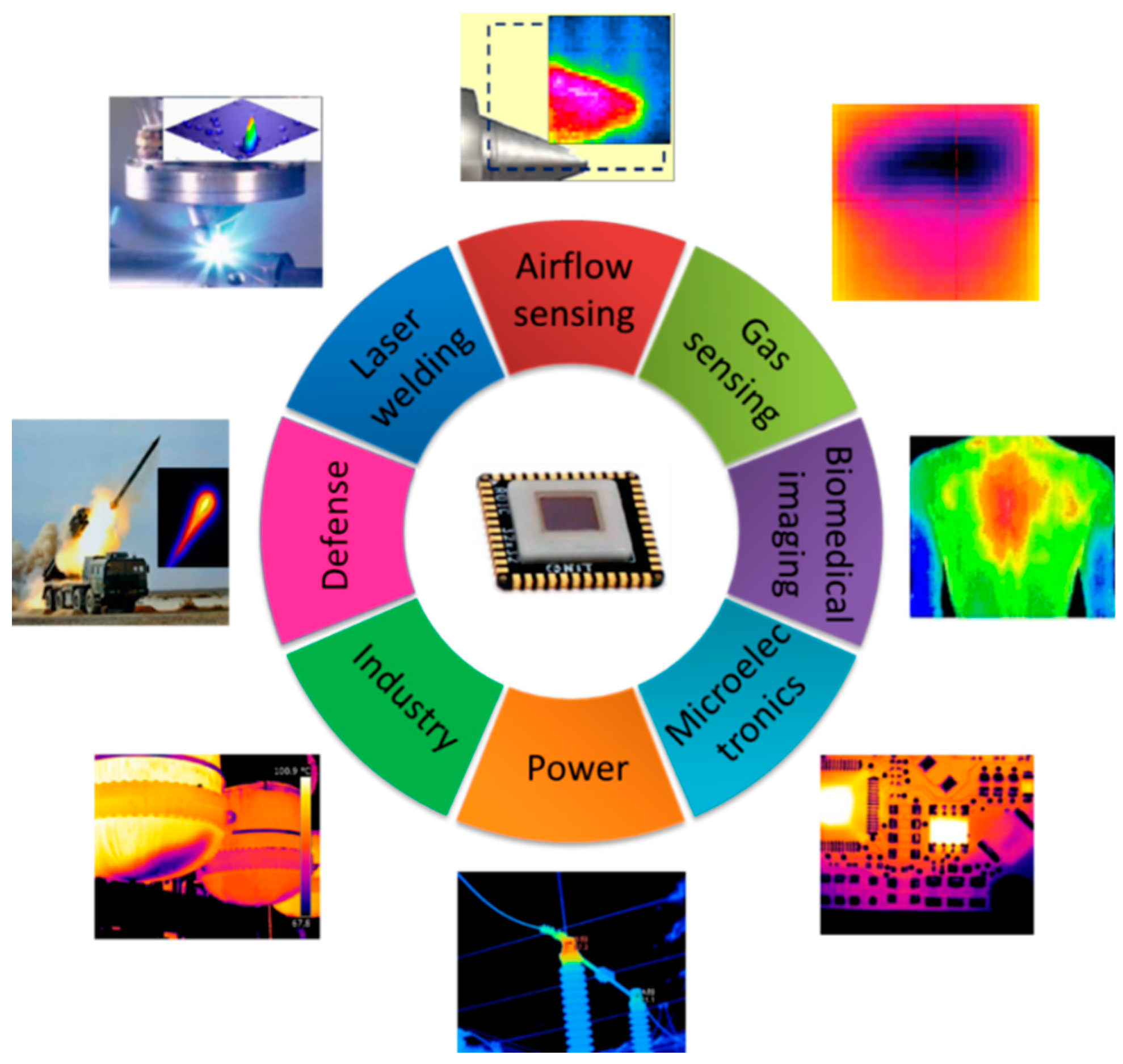
How Can the Optoelectronic Sensitization Enable Photosensitivity Enhancement Without Cooling?

Generally, the physical properties—including optical, electrical, and optoelectronic—of a photodetector are highly dominated by the structural and compositional properties of the material, which are determined by the preparation conditions and parameters. The optoelectronic performance of a photodetector is usually defined using the responsivity and the specific detectivity. The responsivity of a photoconductor can be expressed as
R ( λ ) = η λ τ V b A d h c n 0
where η is the internal quantum efficiency (IQE), λ is the wavelength, τ is the minority carrier lifetime, Vb is the bias voltage, A is the detector area, d is the thickness of the material, h is the Planck constant, c is light speed in vacuum, and n0 is the free carrier concentration [53]. Thus, the specific detectivity can be calculated by
D * = R ( λ ) ( A Δ f ) 1 / 2 V n
where Δf is the frequency bandwidth, and Vn is the rms noise voltage [51]. To improve the optoelectronic performance, the signal-to-noise ratio should be improved, but is hard to achieve at room temperature, since thermally excited carrier concentration and the carrier fluctuations are significant and comparable with the photogenerated carrier concentration at room temperature due to the narrow bandgap. An easy approach is cooling the photodetector platform to reduce the thermally induced noise signal and free carrier concentration, which are usually positively correlated. This cooling method uses thermoelectric cooler (TEC) or another cooling platform, which requires ultra-power, and makes the detector non-portable and complicated.
Another method is to improve the minority carrier lifetime that can be determined by another parameter: the photoconductive gain factor
G = ( τ n μ n + τ p μ p ) V b l 2
where τn and τp are the lifetime of the electrons and holes, respecitvely; μn and μp are the mobility of electrons and holes, respectively; and l denotes the electrode distance. It is seen that the G factor is affected by the carrier transport properties and the design of detector electrodes. An easy approach to improve the carrier lifetime is doping the near deep energy-level elements into the material to construct the minority carrier traps, which capture minority carriers and then release them. Oxygen has been found to be the proper one, and it can be diffused into the PbSe crystal lattice and activated by annealing at about 400 °C. Another effect of annealing in oxygen atmosphere is the material passivation by which the structural defects are passivated, and the free carrier concentration (n0) and the dark current are reduced. Therefore, the responsivity is highly enhanced to enable the photodetector to be much more sensitive to the infrared radiation without cooling. This is the initial motivation of the optoelectronic sensitization of the lead chalcogenides. The PbSe material after sensitization exhibits a polycrystalline structure with an average crystallite size of hundreds of nanometers.
Another sensitization technology is halogen treatment, which can further passivate the material to reduce the dark current, and is proven to be prone to highly improve the potential barrier height between crystallites, as well as be superior to oxygen [54]. A high potential barrier height between crystallites can reduce the dark current and the noise signal to further improve the specific detectivity of the photodetector, since the thermally excited carriers don’t have enough energy to move across the crystallite boundary barrier. These effects make the PbSe polycrystalline coatings able to work at room temperature (300 K) without cooling.

2. Optoelectronic Sensitization Models toward Physical Mechanisms

To exploit the physical mechanism of optoelectronic sensitization, many models have been presented. These models can be generally divided into four classes: the minority carrier trap model, the barrier model, the generalized model, and charge separation junction models. Each model describes a potential mechanism of carrier transport, although there may be multiple mechanisms in the PbSe polycrystalline coatings. Furthermore, the model referred to physical issues that are hard to be verified by experimental observations or theoretical calculations. Nevertheless, the specific parameters of the physical properties calculated by the models can be almost consistent with the experimental characterizations. Therefore, more experimental observations and verifications on a micro level such as structural defects, carrier transport, and crystal growth, and theoretical calculations on band structure using density functional theory (DFT) and the Monte Carlo method, should be performed to exploit or verify the physical mechanisms in the PbSe polycrystalline coatings.

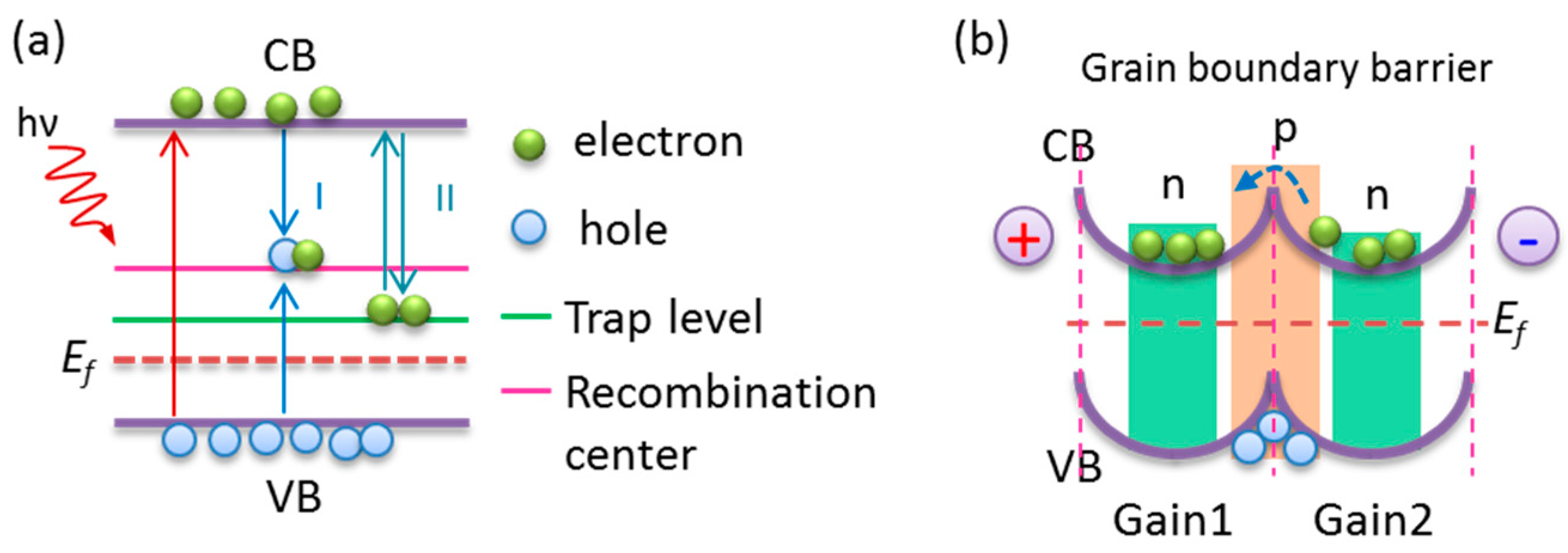
2.1. The Minority Carrier Trap Model

By doping near deep-level oxygen atoms into the crystal lattice of PbSe, a minority carrier trap level could be introduced into the band gap. Humphrey and Petritz suggested that a (PbO)+ generated by a (PbO)++ acceptor level after sensitization with oxygen may serve as an electron trap [55]. When the photons are absorbed, the electron–hole pairs are excited. Some electron–hole pairs recombine immediately, while some other electrons are trapped by the trap level, as shown in Figure 2a. The untrapped electrons will recombine with holes at the recombination center in a very short time of about tens of nanoseconds (process I), which is known as Shockley–Read–Hall (SRH) recombination. The trapped electrons should be released to the conduction band before recombination (process II). However, the release process is much slower than recombination within about serval microseconds. So, the minority carrier (electron) lifetime will be improved and enhance the responsivity of the photodetector, since the surface layer of the PbSe polycrystalline coating will be converted from n-type to p-type after sensitization with oxygen. This model can coherently explain the carrier lifetime improvements, but the minority carrier trap energy level and the composition have not been verified by experimental observations. Recently, a preliminary theoretical band diagram calculation by DFT was performed for the oxygen/iodine-doped crystal cell, showing that an acceptor level exists and may act as a hole trap by accepting an electron [54]. However, this calculation result exhibits a difference in carrier trap type. Any refined theoretical or experimental attempts should be made to verify or refute the carrier trapping mechanism.

2.2. The Barrier Model

Slater found that the temperature dependence of the electrical conductivity follows a linear relationship between lnσ and 1/T (Arrhenius behavior) [56]. Hence, he claimed that the grain boundary barrier exists between neighboring grains, and is caused by an n–p–n type region around the grain boundary, as shown in Figure 2b. Horn also pointed out that the grain boundary is surrounded by PbO to form a p–n heterojunction between grains in the PbSe polycrystalline coatings after sensitization [57]. This model suggests that the high resistance after sensitization is attributed to the grain boundary barrier, since free electrons are hard to move from a grain to another under a bias voltage, as shown in Figure 2b. However, the increase in photoconductivity is attributed to the decline of the barrier height due to the photogenerated carriers. The study on carrier transport from the recent literature found that the carrier transport indeed obeys the Arrhenius thermally-driven behavior at high temperature of >210 K, while an obvious deviation from the Arrhenius behavior occurs at low temperature of <210 K [54]. Therefore, there should be another transport mechanism that dominates the carrier transport and electrical conductivity at low temperatures.

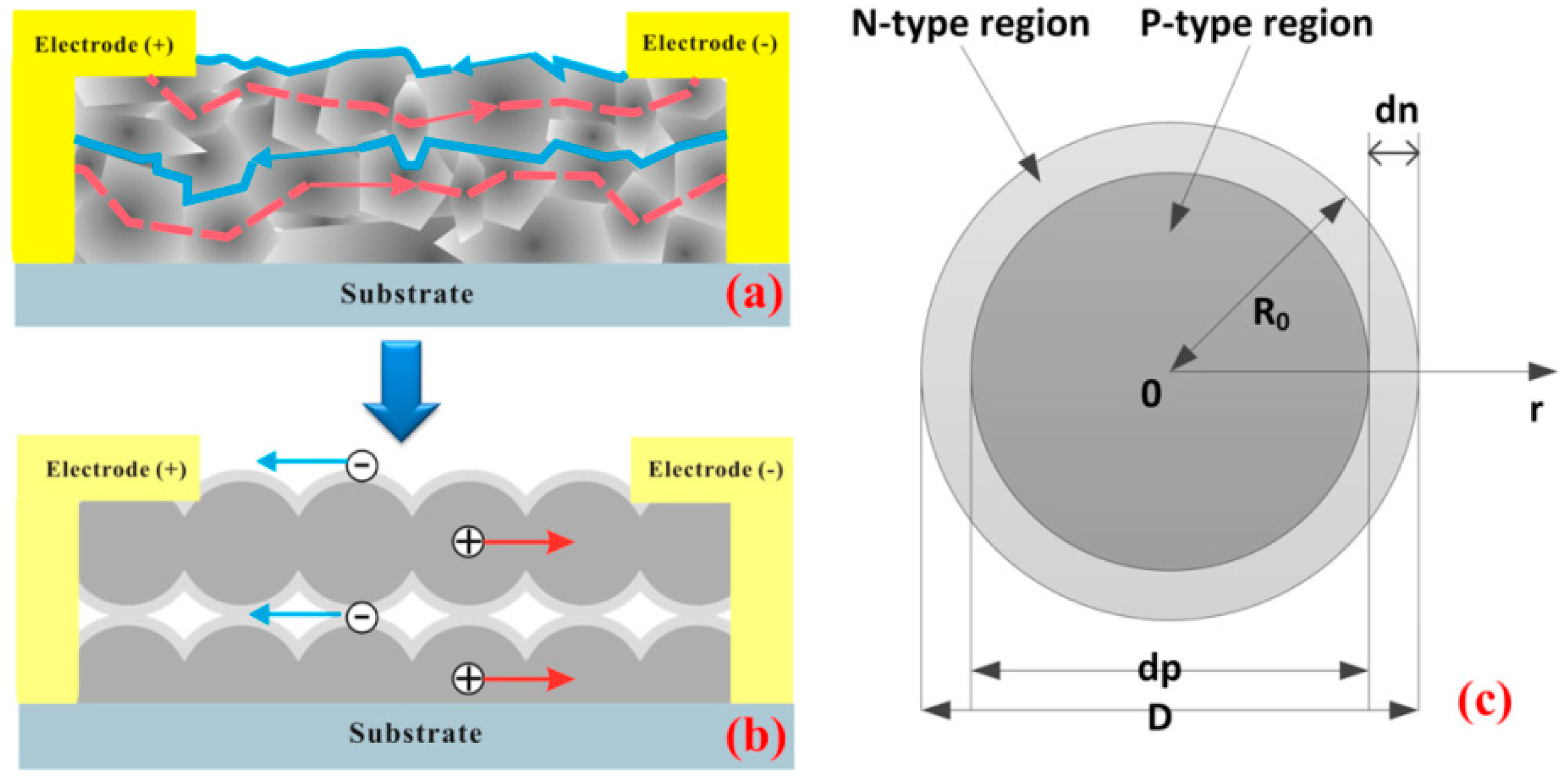
2.3. The Generalized Model

Considering the density of photogenerated carriers and the grain boundary barrier, Petrtiz presented a model that is similar to that of bulk material [58]. It suggests the electrical conductivity of the PbSe polycrystalline coating is the sum of that of every crystallite, and the photoconductivity enhancement is attributed to the variation of carrier mobility that depends on the grain boundary barrier. Likewise, the noise and sensitivity limit were also deduced. This model is mathematically coherent, and similar with that for polycrystalline silicon [59,60,61]. Unfortunately, no one has claimed that the experimental data is always in good agreement with this model until now. Some oriented experiments including measuring the minority carrier concentration and lifetime, quantum efficiency, majority carrier concentration, and mobility by the Van der Pauw method, responsivity, and noise voltage can perhaps be carried out to verify this model.

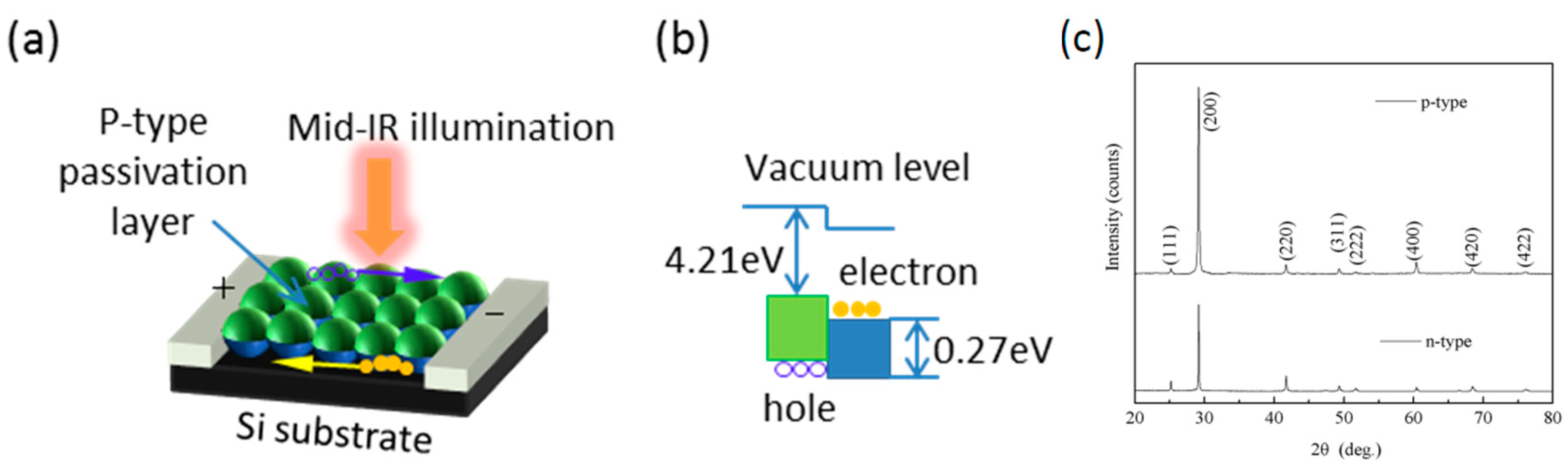
2.4. The Charge Separation Junction Model

This model was presented by Zhao et al. and has been accepted by many researchers, including us [62]. This model also supports the p–n junction region around the surface of the crystallites, which contains the oxides and iodides of PbSe, exhibiting an n-type conductive nature. On the contrary, it claims that the photogenerated carriers are just separated by the p–n junction into the corresponding channels (n-channel for electrons, p-channel for holes), and few carriers choose to move across the grain boundary barrier when biased [63], which is different from the previous p–n junction and barrier models [56,57]. Electrons move along the surface of crystallites, and holes move along the core of crystallites, since the neighboring crystallites will fuse and connect together, as shown in Figure 3. The separation of the photogenerated carrier leads to an improvement of the minority carrier lifetime. According to this model, the carrier concentration distribution in the crystallites, minority carrier lifetime, and resistance after sensitization were calculated. The shell microlayer of the crystallites was designated to be n-type, because iodine was assumed to be an n-type dopant for PbSe, which is completely different from the oxygen/halogen-induced p-type conductivity reported in the literature [52]. Furthermore, the previous works on the conductive types of PbSe polycrystalline coatings also revealed that only the as-grown PbSe thin film in n-type can trigger optoelectronic enhancement after sensitization, which implicitly supports the existence of the charge separation p–n junction, combining with the p-type shell of crystallites [64]. Unfortunately, the core/shell p–n junction structure and the carrier transport channels seem to be hard to verify experimentally. Perhaps the high-resolution scanning photocurrent imaging may be promising to observe the carrier transport channels [65,66].

3. Fabrications and Properties of the PbSe Polycrystalline Coatings

We now discuss the physical properties of PbSe polycrystalline coatings prepared by different fabrication technologies, and their possible connections with the physical mechanisms of structural evolution, carrier transport, optical absorbance, and optoelectronic enhancement.

3.1. The Functional Effects Induced by Oxygen Treatment

The oxygen treatments on the monocrystalline PbSe coating fabricated by molecular beam epitaxy (MBE) at different temperatures were performed by Zhao et al. [67]. They discovered that the oxygen treatment has a passivation effect on the carrier recombination in the PbSe polycrystalline coating, revealed by using the photoluminescence (PL) spectra operated at room temperature and 77 K, and the X-ray photoelectron spectroscopy (XPS) spectra, as shown in Figure 4. A high PL intensity revealed that the surface recombination and non-radiative recombination mechanisms, including Auger and SRH, were significantly inhibited after oxygen treatment, indicating that the surface states and the deep energy level recombination centers were passivated to improve the minority carrier lifetime and optoelectronic performance eventually. These results may be very useful for understanding the structural modification of the surface functional layer of the polycrystalline lead chalcogenides, and manufacturing ultrasensitive mid-infrared uncooled photodetectors [68,69]. Likewise, another study on the effect of oxygen treatment on the evaporated n-type PbSe coatings was also carried out, and focused on the impact of electrical conductive type on the structural, compositional, electrical, and optoelectronic properties [64]. Another effect of electrical conductive-type dependence of optoelectronic performance was discovered, and could be a direct experimental support for the charge separation model [62], as shown in Figure 5.

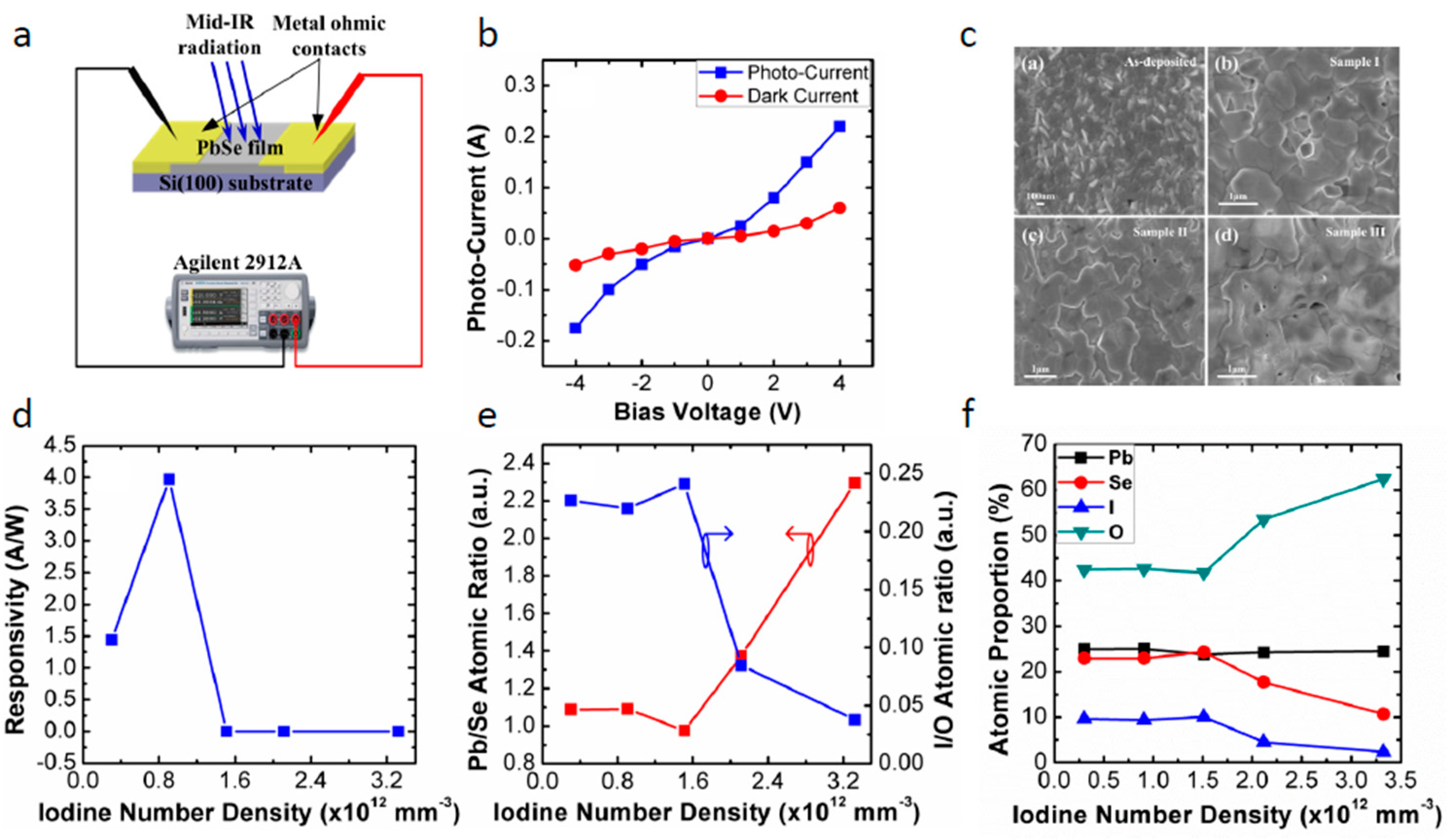
3.2. The Iodination Impact on the Photosensitivity

Iodine was verified to be another sensitizer for lead chalcogenides. Torquemada et al. reported that halogen only serves as a transport improver during the PbSe recrystallization in their work of thermally deposited PbSe treated with iodine years ago, which promotes the in situ incorporation of oxygen into the PbSe crystal lattice in an electrically active position [70,71,72,73,74]. However, Qiu et al. pointed out that it is iodine that triggers the photosensitivity of PbSe [75], compared with oxygen, by performing a variety of annealing experiments using nitrogen/oxygen/iodine single or hybrid atmosphere, as shown in Figure 6. A more blunted and coalescent boundary structure was observed after the iodination process, as shown in Figure 6a. The presence of PbSeO3 (301), as a result of the oxygen passivation, was revealed to be responsible for the optoelectronic enhancement of PbSe polycrystalline coatings, as shown in Figure 6b. It was stated that iodine is prone to decrease the PL intensity and increase the resistance of the p-type PbSe polycrystalline coatings, indicating that iodine will incorporate into the PbSe lattice, but the incorporated concentration could be very low [75].
The optoelectronic measurements indicated that the highest specific detectivity of 2.8 × 10¹⁰ Jones was obtained from their sample treated by 25 min of oxygen followed by five minutes of iodine, and was attributed to the combination of oxygen passivation and iodine incorporation [76]. Oxygen otherwise was revealed to serve as an improver to aid iodine incorporating into the PbSe lattice and a passivation agent to passivate structural defects such as Pb vacancies, as shown in Figure 6b,c. Low PL intensities in the iodized PbSe polycrystalline coatings may be attributed to the high surface recombination rate of minority carriers; this may be caused by the coalescent boundary in morphology, which introduces a lot of surface states again after iodination. These results promote a new understanding of the relationship between oxidation and iodination in the PbSe polycrystalline coatings.

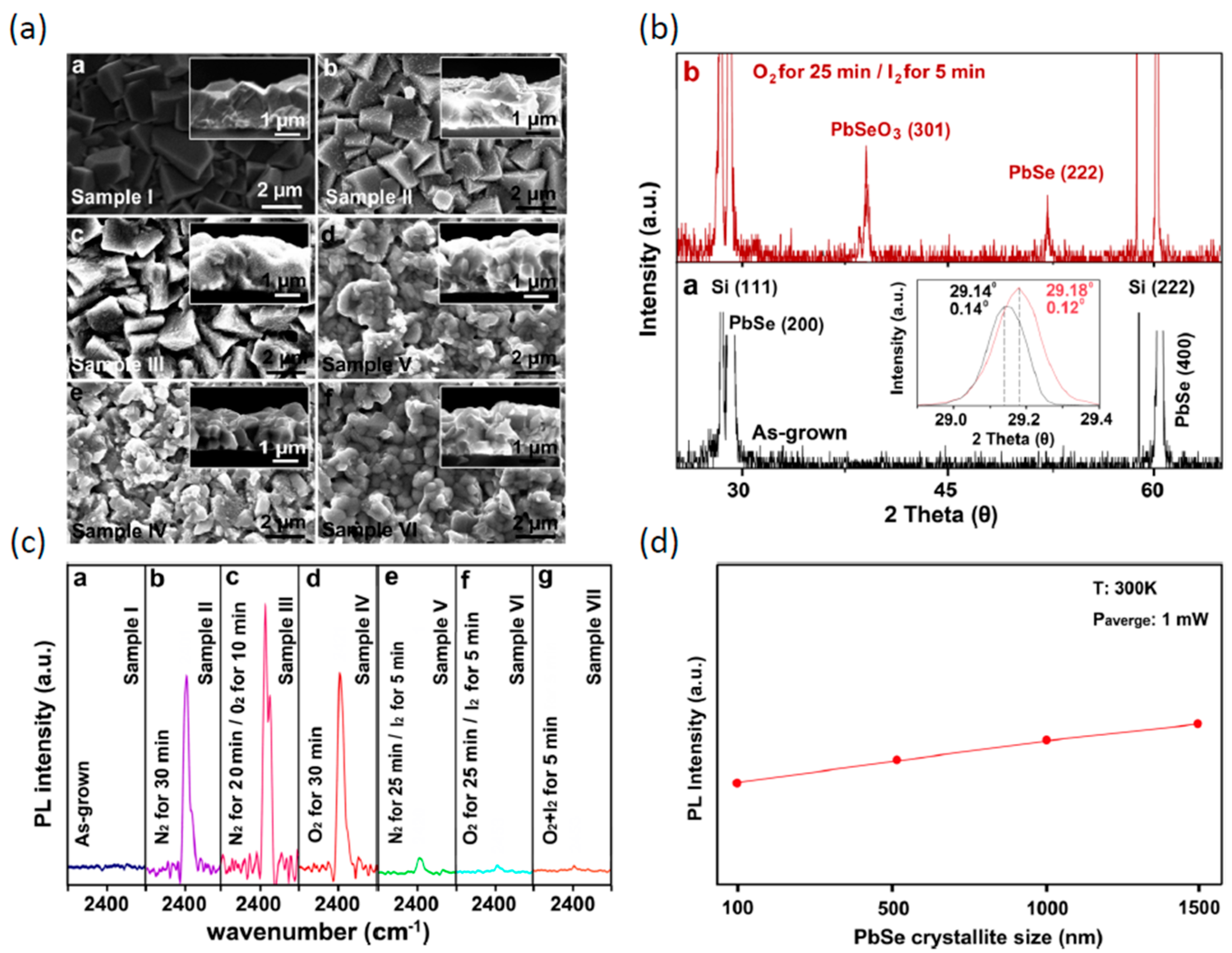
3.3. Stoichiometric Optimization via Iodine Concentration Regulation

Another work on iodination effect was carried out to fabricate the material by changing the iodine concentration, as shown in Figure 7, indicating that it is possible to manipulate the inherent stoichiometry of PbSe polycrystalline coatings via controlling the iodine concentration during the sensitization process [77]. It was revealed that the Pb/Se atomic ratio can be modulated by the I/O atomic ratio to change the stoichiometry of the material, as shown in Figure 7e. As is seen, the high responsivity of 3.97 A/W was achieved at the iodine concentration of 9.1 × 1011 mm−3, and a low iodine concentration of <1.5 × 1012 mm−3 was necessary to obtain the high photoelectric performance, as shown in Figure 7d. It was indicated that the significant deviation of the Pb/Se atomic ratio from 1:1 due to over-iodination was responsible for the significant decline of responsivity [73,74]. These results present a new role for halogens in the sensitization mechanism, and provide a direct approach to optimize the photosensitivity of the PbSe polycrystalline coatings at room temperature.

3.4. The Properties of Surface Functional Layer

The surface structure of PbSe polycrystalline coatings prepared by oxygen/iodine diffusion is an inexplicable issue due to the complexity of phases and crystalline structures. In the following sections, we introduce the characterization results and discoveries from the work reported by Kumar et al., since they made a comprehensive study on the phase and structural properties.

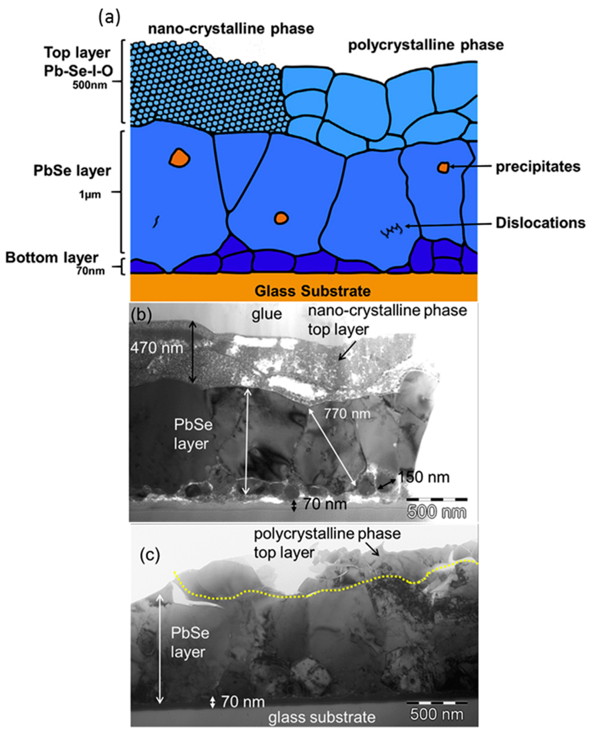
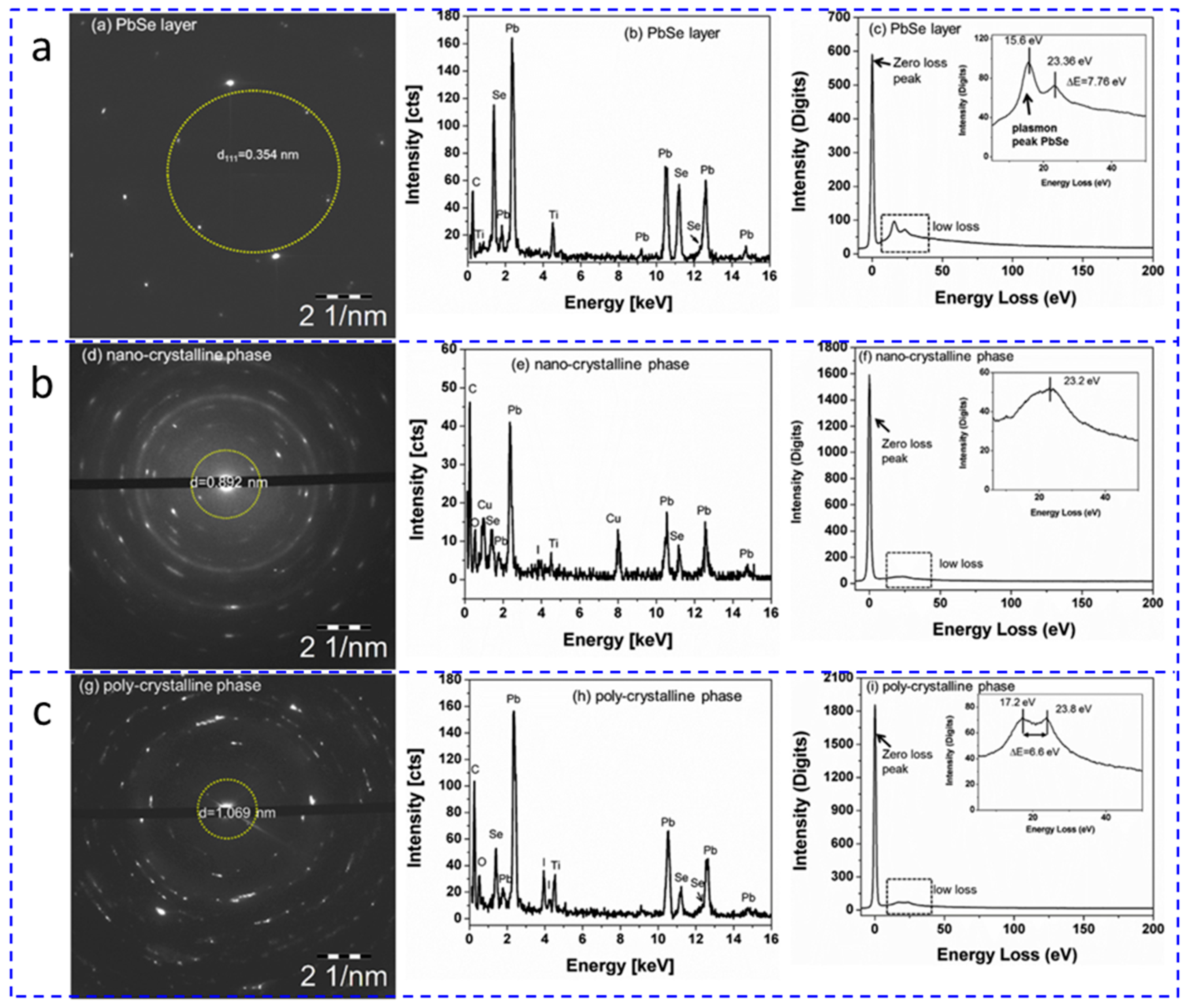
3.4.1. Phase Analysis

A further investigation on the surface phase analysis of PbSe polycrystalline coatings was made using selected area electron diffraction patterns (SAED), electron energy-loss spectroscopy (EELS), and energy-dispersive X-ray spectroscopy (EDX) by Kumar et al. [78]. They showed in detail that the PbSe polycrystalline coating after oxygen/iodine sensitization should consist of a bottom layer of PbSe and a top layer of Pb–Se–O–I, which can be divided into a polycrystalline and a nanocrystalline phase, as shown in Figure 8. The high iodine mole fraction of ~20 at % in the polycrystalline phase and that of <10 at % in the nanocrystalline phase were revealed by EDX characterizations via the Cliff–Lorimer method [79,80]. The nanocrystalline and polycrystalline phases in the top layer were confirmed by SAED, and exhibited large unit cells and d spacings of 0.892 and 1.069 nm, respectively, as shown in Figure 9. By EELS spectroscopes, the nanocrystalline Pb–Se–O–I phase with a broad plasmon peak centered at about 23.2 eV and the polycrystalline phase with two sharp plasmon peaks at 17.2 and 23.8 eV were distinguished from PbSe with plasmon energy of 15 eV, as shown in Figure 9. They suggested that the Pb–Se–O–I phase is responsible for the high photosensitivity of iodized PbSe polycrystalline coatings.

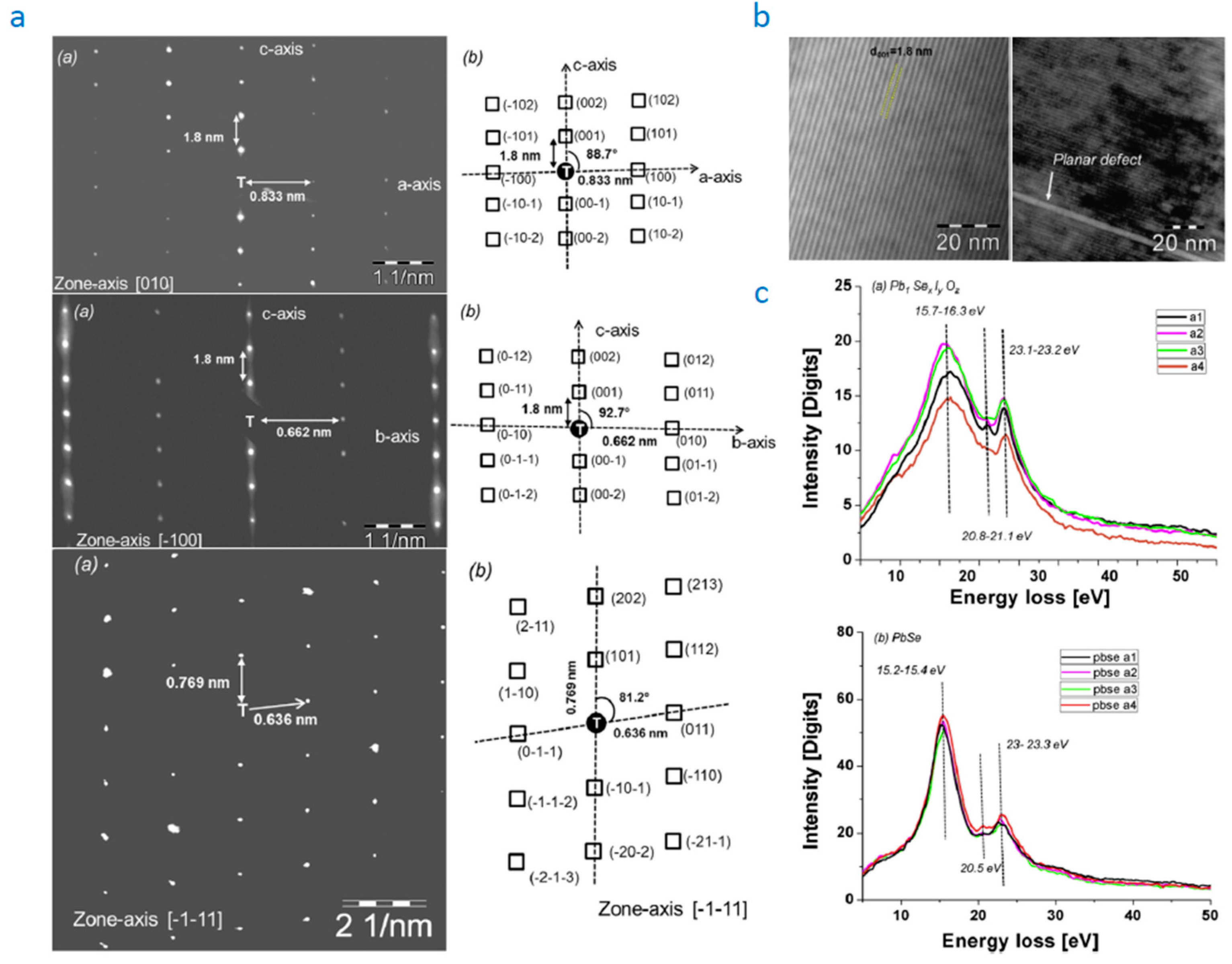
3.4.2. Structural Analysis

Another investigation of the surface structural properties was carried out by SAED, high-resolution transmission electron microscopy (HRTEM), EDX, and low loss EELS [81]. A pseudo-orthorhombic Bravais lattice of the PbSexIyOz phase of the top layer with lattice parameters of a = 0.833 nm, b = 0.662 nm, and c = 1.8 nm was eventually identified via energy-filtered SAED patterns in the [100], [010], and [111] poles, as shown in Figure 10a. The lattice parameter of c = 1.8 nm was confirmed by the high-resolution transmission electron microscopy (HRTEM) images, as shown in Figure 10b. The chemical composition of the quaternary phase PbSexIyOz was determined by EDX spectroscopy as 0.17 ≤ x ≤ 0.5 and 0.2 ≤ y ≤ 0.5 in atomic ratio. EELS spectra also proved the presence of the new phase with a double plasmon peak at 15.7–16.3 eV (peak 1) and 23.1–23.2 eV (peak 2), respectively [82], as shown in Figure 10c. These results promote the understanding of surface structure and stoichiometry. However, the role of this new phase in the photosensitivity enhancement needs further verifications experimentally.

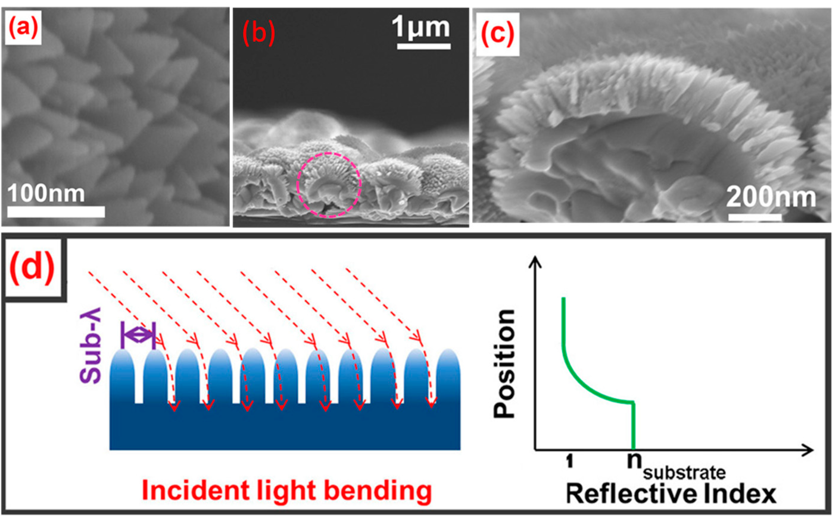
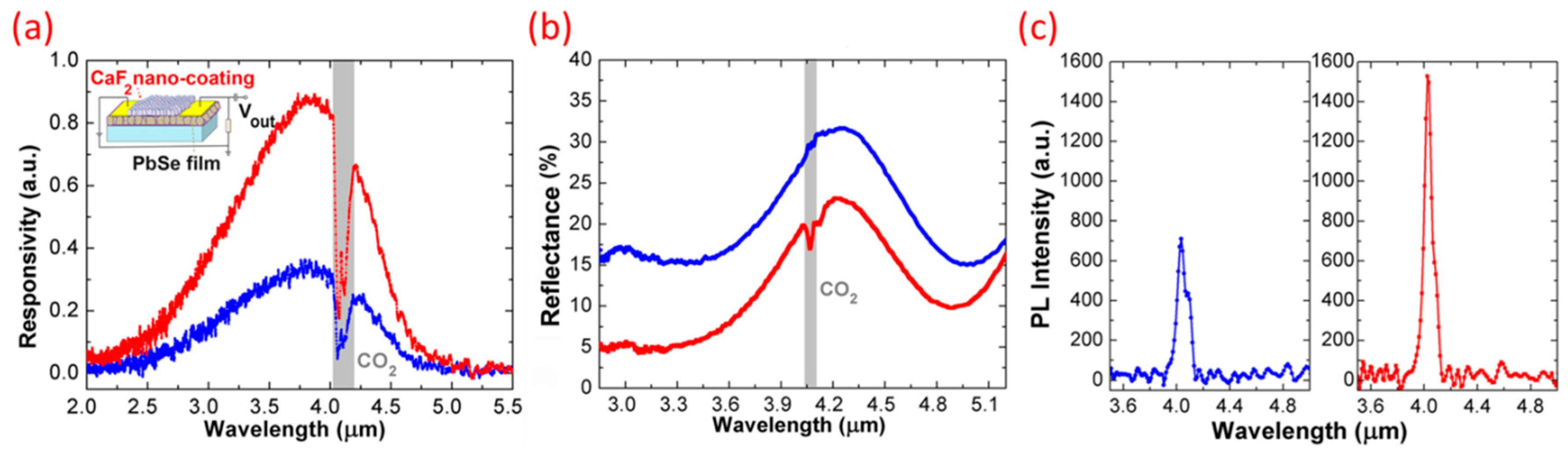
3.5. Growth with the Nanostructured Antireflective Coatings

Another approach to further enhance the photoresponsivity of PbSe polycrystalline coatings, as presented by Weng et al., is to use an alkaline earth metal fluoride coating such as CaF2 and BaF2 as an antireflective surface layer [83]. One reason to use it is the epitaxial compatibility with PbSe due to the similar crystal structure and lattice parameters, which can reduce the structural defects caused by lattice mismatch. Another reason is alkaline earth metal fluorides are transparent (~95% transmittance) in a wide range of 0.2–12 μm [84]. Figure 11a–c shows the PbSe polycrystalline film coated by a 200 nm thick CaF2 flower-like nanostructured coating with a tapered shape, which may be attributed to the predominant growth at the (111) plane according to the lowest surface energy mechanism [45,46]. It was revealed that light propagation will be bent by the sub-wavelength dimensional tapered structure to improve the light collection efficiency due to the induced gradient refractive index profile and a convergence effect as convex optical lens [85,86,87,88,89], as shown in Figure 11d.
The optical and the optoelectronic characterizations, including PL, optical reflectance, and responsivity spectra, were carried out by the Fourier transform infrared spectroscopy (FTIR), demonstrating that the photoresponsivity was enhanced by the CaF2 antireflective nanostructured coating to about 200% due to the broadband antireflective effect caused by light bending, as shown in Figure 12a,b. Another effect induced by the CaF2 nanostructured coating is surface passivation, which could decrease the surface recombination of minority carriers [90,91], as indicated by the PL spectra shown in Figure 12c. These effects and mechanisms were predicted to be responsible for the optoelectronic enhancement of this composite structure. These results show a good structural coupling between polycrystalline PbSe and alkaline earth metal fluorides, and provide an effective approach to further improve the optical and optoelectronic performances of photodetectors and light-emitting devices (LEDs) [92,93].

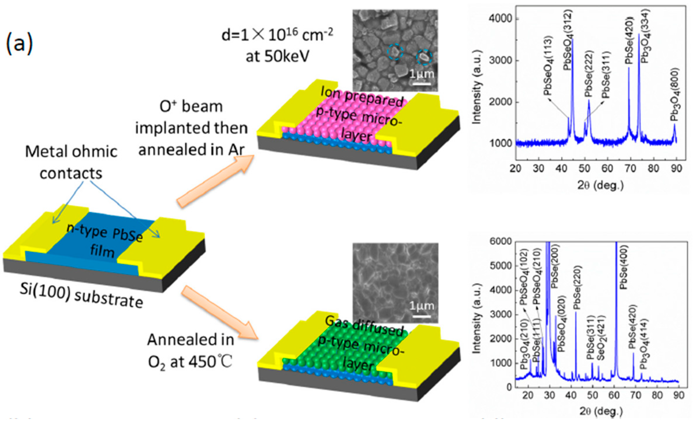
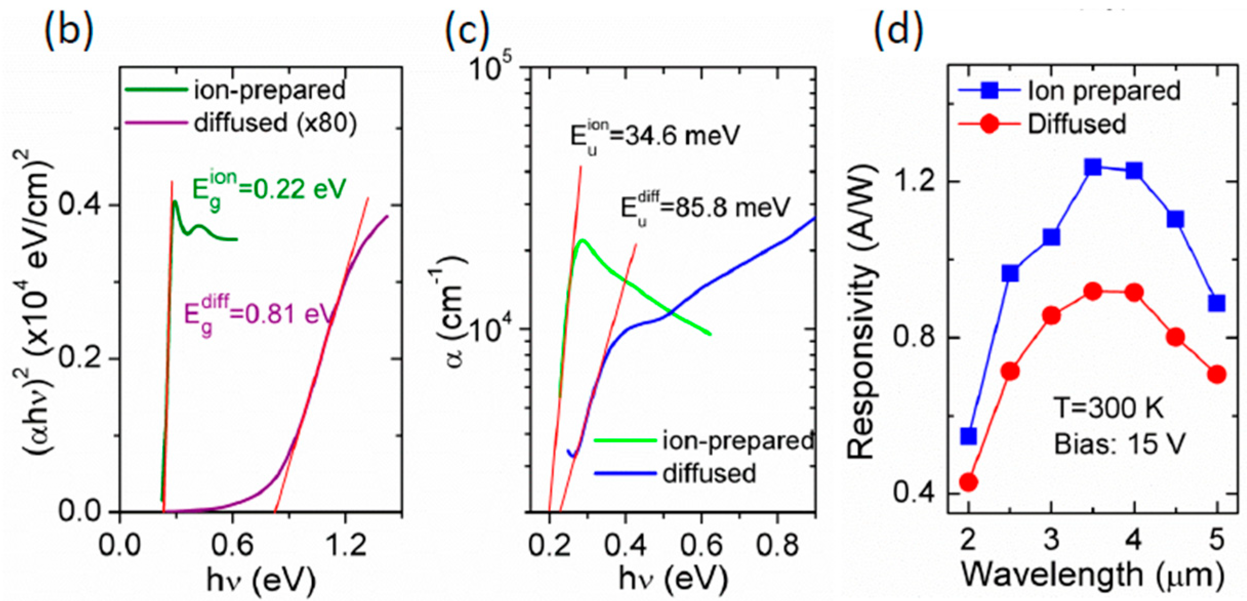
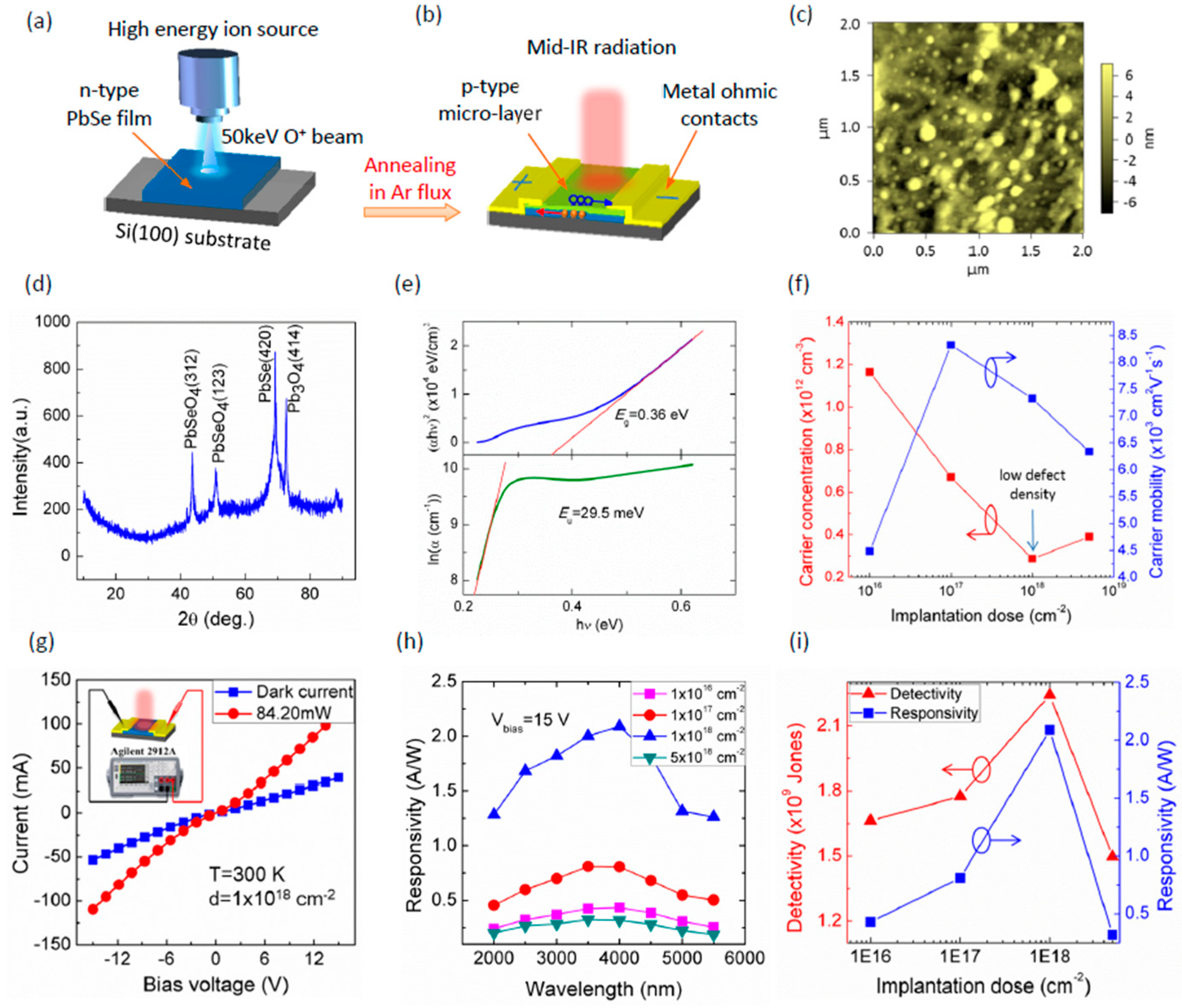
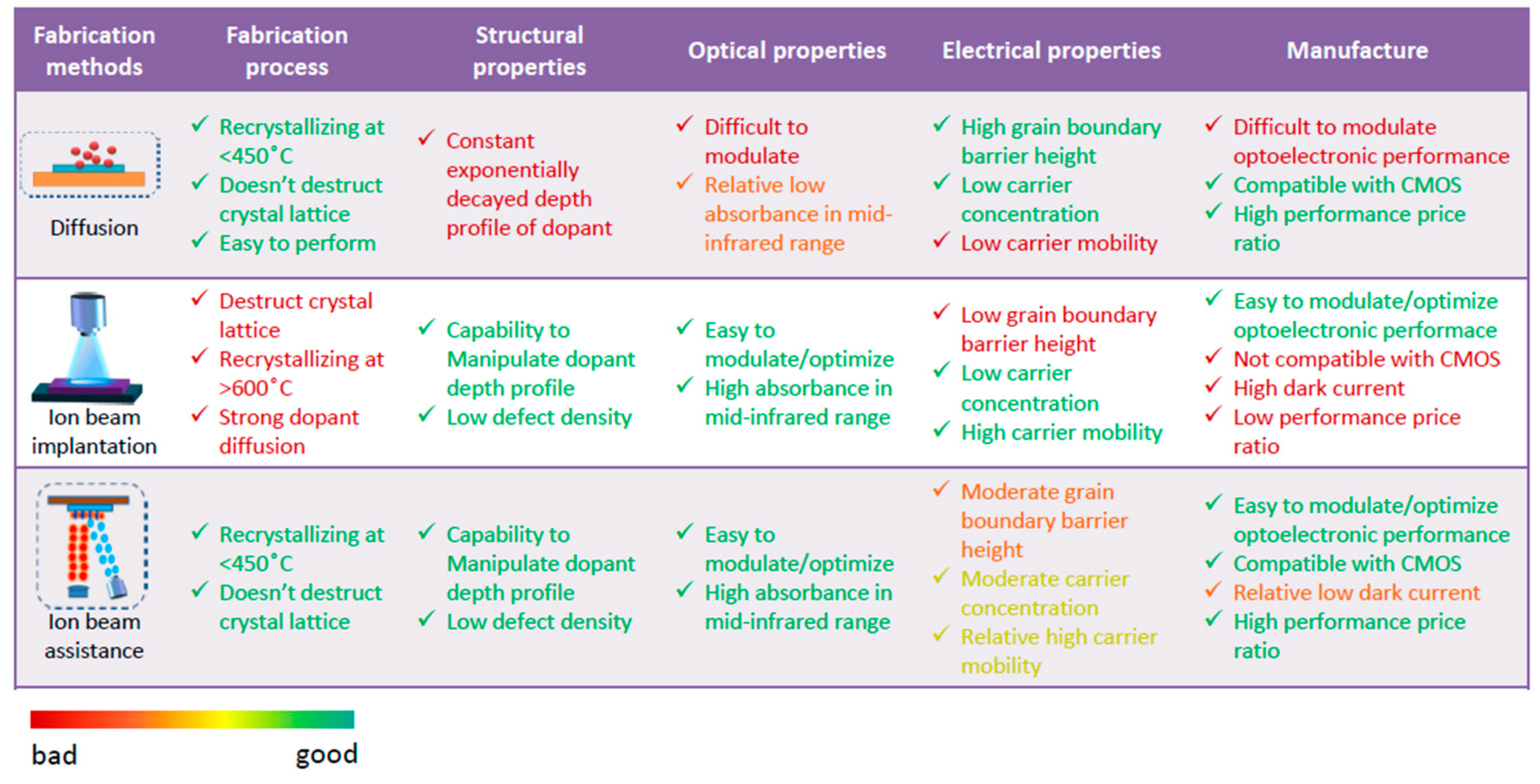
3.6. Preparation via Ion Beam Implantation

The diffusion technologies mentioned above actually provide an easy approach to dope and activate the oxygen/iodine atoms into lead chalcogenides. However, the profile of oxygen/iodine is exponentially decayed along the depth direction, which is constant and mainly prone to modify the surface properties [94,95]. Turning to modify the stoichiometric depth profile of the inner layer is a promising method to modulate/optimize the optical, electrical, and optoelectronic performances of materials [96,97,98,99].
A sensitization technology via O+ beam implantation at 50 keV followed by an annealing process in Ar atmosphere at 600 °C was demonstrated by us recently [100], as shown in Figure 13. Compared with the conventional oxygen diffused counterpart, the preliminary characterizations revealed that the ion beam-prepared PbSe material exhibited a polycrystalline structure with crystallite sizes of 300–700 nm, as shown in Figure 13a. The optical bandgap of 0.22 eV is more suitable for detecting mid-infrared photons, and the low Urbach energy of 34.6 meV indicates a well-ordered crystalline structure with low defect density, leading to higher optical absorption in the mid-infrared range and carrier mobility, which were responsible for the high responsivity of 1.23 A/W at 4 μm, as shown in Figure 13b–d.
Other ion beam preparations were performed with a higher following annealing temperature of 990 °C to further repair the damaged crystal structure [101], as shown in Figure 14a,b. It was revealed that the resulting material is nanocrystalline with high mid-infrared absorption and ultrahigh carrier mobility up to the magnitude of 103 cm2 V−1 s−1 due to the low defect density represented from the low Urbach energy of 29.5 meV [102,103], as shown in Figure 14c–f. It was indicated that the PbSe polycrystalline coatings prepared by ion beam implantation exhibited a high optoelectronic performance that can be modulated by the implantation dose. However, a high dark current was also observed, which limits the improvement of the specific detectivity, as shown in Figure 14g–i. The low size-dependent crystallite boundary barrier height may be responsible for the high dark current, since the free carrier concentration is relatively low due to the deep energy level doping of oxygen [104,105], as shown in Figure 14f. These results show a new approach to synthesize and sensitize PbSe polycrystalline coatings for high optical, electrical, and optoelectronic performances. More fundamental researches on how the dark current could be affected by carrier transport and how the electrical performance can be optimized by tuning the ion beam parameters, e.g., ion energy, should be considered to further explore the potential of these ion beam-prepared PbSe polycrystalline coatings.

4. Interesting Areas, Challenges, and Perspectives

4.1. Electrical Properties

The electrical properties have a close relation with the optical and optoelectronic properties. Although there are many comprehensive studies on PbSe polycrystalline coatings, a deep focus on the electrical properties such as the carrier transport mechanism, impurities, defects, and their impact on the carrier transport, and the fine electronic structure has rarely been reported in recent years. Especially, the carrier transport mechanism at low temperature is unclear [54]. Furthermore, deep-level impurities and defects (including vacancies, dislocations, stacking faults, etc.) can form non-equilibrium carrier traps or recombination centers. The characterizations on the concentration distribution, compositional identification, and the capture cross-section of the trap centers are important to understand the carrier transport and recombination mechanisms [47,106,107]. However, these characterizations seem to be difficult to perform, because they need more complex analysis to extract the physical mechanisms from limited experimental characterizations. The thermally stimulated current (TSC) spectroscopy and low temperature Hall effect measurement may be promising to exploit the mysterious electrical properties of PbSe polycrystalline coatings.

4.2. Growth Mechanism-Related Calculations

Growth mechanism on the morphological evolution, preferred growth orientation, the surface energy minimization, and defect formation, as well as the relation with the influencing factors such as preparation conditions, is another interesting area, which can be important to understand the crystal growth mechanism and effectively control the repeatability and reliability of the preparation technology. Recently, the growth mechanism of evaporated PbSe based on the Gibbs free energy variation minimization was calculated via DFT by Sun et al., which explained the preferred growth orientation of (200) for evaporated PbSe film on the Si substrate [45,46]. This is a good beginning for understanding the growth mechanism of PbSe polycrystalline material.

4.3. New Preparation Technologies

Another interesting area is developing new preparation methods for exploring new physical properties and mechanisms. As mentioned above, ion beam technology exhibits a variety of advantages, but also has drawbacks such as a high dark current and low performance/price ratio. A novel ion beam-assisted preparation method may be promising. Unlike the ion implantation, ion beam assistance doesn’t damage the crystal lattice. Therefore, a high temperature (>600 °C) annealing is unnecessary. The preliminary characterizations demonstrate that this technology exhibits the advantages that ion beam implantation has, as well as a high performance/price ratio. Figure 15 has summarized the properties of this technology with comparisons with currently developed technologies. As is seen, this ion beam-assisted method almost combines the advantages of ion beam implantation and diffusion technologies. Moreover, the improvements of other preparation methods such as CBD and RF magnetron sputtering are also attractive for the preparation of PbSe polycrystalline coatings for high optical, electrical, and optoelectronic performances.

4.4. Compounding with Other Materials and Structures

Constructing composite materials and nanostructures with metasurfaces, two-dimensional (2D) materials, and carbon nanotubes is another predictable development area, which enables taking advantage of the specific properties of these materials and structures. Coating with a metasurface can improve the optical absorbance intensively at a specified wavelength according to the induced SPR effect, which is very useful to enhance the internal quantum efficiency and the optoelectronic performance. Compounding with 2D materials such as graphene is another attractive technology for high-speed applications due to the high carrier mobility in graphene. These composite materials can highly expand the applications of PbSe polycrystalline coatings for novel properties and devices in optoelectronics.

5. Summary

In summary, we have discussed the initial motivation to make PbSe bulk material sensitive to mid-infrared radiation without cooling. Then, several physical models are introduced to explain and understand why the optoelectronic enhancement is possible. The structural, compositional, optical, electrical, and optoelectronic properties, as well as the corresponding physical effects of PbSe polycrystalline coating prepared by different diffusion and ion beam technologies, are discussed in detail, which show huge optical and optoelectronic potentials in this material. Finally, the interesting areas, challenges, and perspectives for novel hybrid optoelectronic devices, physical effects, and applications are also discussed. These devices and properties make PbSe polycrystalline material more attractive in the applications of high-speed, low-cost, and high-performance optical and optoelectronic devices.

Author Contributions

Conceptualization, H.Y. and J.Z.; Methodology, J.Z.; Investigation, X.L. and G.W.; Writing—Original Draft Preparation, H.Y.; Writing—Review & Editing, H.Y. and J.Z.; Funding Acquisition, H.Y.

Funding

This work is supported by the National Natural Science Foundation of China (No. 61505166), Natural Science Basic Research Plan in Shaanxi Province of China under Program (No. 2015JQ6244) and the Fundamental Research Funds for the Central Universities (No. 3102015ZY098).

Conflicts of Interest

The authors declare no conflict of interest.

References

  1. Tabachnyk, M.; Ehrler, B.; Gelinas, S.; Bohm, M.L.; Walker, B.J.; Musselman, K.P.; Greenham, N.C.; Friend, R.H.; Rao, A. Resonant energy transfer of triplet excitons from pentacene to PbSe nanocrystals. Nat. Mater. 2014, 13, 1033–1038. [Google Scholar] [CrossRef] [PubMed]
  2. Sykora, M.; Koposov, A.Y.; McGuire, J.A.; Schulze, R.K.; Tretiak, O.; Pietryga, J.M.; Klimov, V.I. Effect of Air Exposure on Surface Properties, Electronic Structure, and Carrier Relaxation in PbSe Nanocrystals. ACS Nano 2010, 4, 2021–2034. [Google Scholar] [CrossRef] [PubMed]
  3. Tisdale, W.A.; Williams, K.J.; Timp, B.A.; Norris, D.J.; Aydil, E.S.; Zhu, X.Y. Hot-Electron Transfer from Semiconductor Nanocrystals. Science 2010, 328, 1543–1547. [Google Scholar] [CrossRef] [PubMed]
  4. Sliem, M.A.; Chemseddine, A.; Bloeck, U.; Fischer, R.A. PbSe nanocrystal shape development: Oriented attachment at mild conditions and microwave assisted growth of nanocubes. CrystEngComm 2011, 13, 483–488. [Google Scholar] [CrossRef]
  5. Schaller, R.D.; Klimov, V.I. High efficiency carrier multiplication in PbSe nanocrystals: Implications for solar energy conversion. Phys. Rev. Lett. 2004, 92, 186601. [Google Scholar] [CrossRef] [PubMed]
  6. Liu, Y.; Gibbs, M.; Puthussery, J.; Gaik, S.; Ihly, R.; Hillhouse, H.W.; Law, M. Dependence of Carrier Mobility on Nanocrystal Size and Ligand Length in PbSe Nanocrystal Solids. Nano Lett. 2010, 10, 1960–1969. [Google Scholar] [CrossRef]
  7. Casavola, M.; van Huis, M.A.; Bals, S.; Lambert, K.; Hens, Z.; Vanmaekelbergh, D. Anisotropic Cation Exchange in PbSe/CdSe Core/Shell Nanocrystals of Different Geometry. Chem. Mater. 2012, 24, 294–302. [Google Scholar] [CrossRef]
  8. Skelton, J.M.; Parker, S.C.; Togo, A.; Tanaka, I.; Walsh, A. Thermal physics of the lead chalcogenides PbS, PbSe, and PbTe from first principles. Phys. Rev. B 2014, 89, 205203. [Google Scholar] [CrossRef] [Green Version]
  9. Akselrod, G.M.; Weidman, M.C.; Li, Y.; Argyropoulos, C.; Tisdale, W.A.; Mikkelsen, M.H. Efficient Nanosecond Photoluminescence from Infrared PbS Quantum Dots Coupled to Plasmonic Nanoantennas. ACS Photonics 2016, 3, 1741–1746. [Google Scholar] [CrossRef]
  10. Sadeghi, H.; Zolanvar, A.; Ranjgar, A. Effective dielectric constant of metal chalcogenides Ag-PbSe nanocomposite. Armen. J. Phys. 2014, 7, 75–86. [Google Scholar]
  11. Segets, D.; Lucas, J.M.; Taylor, R.N.K.; Scheele, M.; Zheng, H.M.; Alivisatos, A.P.; Peukert, W. Determination of the Quantum Dot Band Gap Dependence on Particle Size from Optical Absorbance and Transmission Electron Microscopy Measurements. ACS Nano 2012, 6, 9021–9032. [Google Scholar] [CrossRef] [PubMed]
  12. Jasieniak, J.; Califano, M.; Watkins, S.E. Size-Dependent Valence and Conduction Band-Edge Energies of Semiconductor Nanocrystals. ACS Nano 2011, 5, 5888–5902. [Google Scholar] [CrossRef]
  13. Feng, W.R.; Zhou, H.; Chen, F. Impact of thickness on crystal structure and optical properties for thermally evaporated PbSe thin films. Vacuum 2015, 114, 82–85. [Google Scholar] [CrossRef]
  14. Arivazhagan, V.; Parvathi, M.M.; Rajesh, S. Impact of thickness on vacuum deposited PbSe thin films. Vacuum 2012, 86, 1092–1096. [Google Scholar] [CrossRef]
  15. Kityk, I.V.; Demianiuk, M.; Majchrowski, A.; Ebothe, J.; Siemion, P. IR-induced second-harmonic generation in PbSe microcrystallites. J. Phys. Condens. Matter 2004, 16, 3533–3544. [Google Scholar] [CrossRef]
  16. Moreels, I.; Hens, Z.; Kockaert, P.; Loicq, J.; Van Thourhout, D. Spectroscopy of the nonlinear refractive index of colloidal PbSe nanocrystals. Appl. Phys. Lett. 2006, 89, 193106. [Google Scholar] [CrossRef] [Green Version]
  17. Wei, K.H.; Fan, S.H.; Chen, Q.G.; Lai, X.M. Passively mode-locked Yb fiber laser with PbSe colloidal quantum dots as saturable absorber. Opt. Express 2017, 25, 24901–24906. [Google Scholar] [CrossRef]
  18. Luther, J.M.; Gao, J.B.; Lloyd, M.T.; Semonin, O.E.; Beard, M.C.; Nozik, A.J. Stability Assessment on a 3% Bilayer PbS/ZnO Quantum Dot Heterojunction Solar Cell. Adv. Mater. 2010, 22, 3704–3707. [Google Scholar] [CrossRef]
  19. Nozik, A.J.; Beard, M.C.; Luther, J.M.; Law, M.; Ellingson, R.J.; Johnson, J.C. Semiconductor Quantum Dots and Quantum Dot Arrays and Applications of Multiple Exciton Generation to Third-Generation Photovoltaic Solar Cells. Chem. Rev. 2010, 110, 6873–6890. [Google Scholar] [CrossRef] [PubMed]
  20. Beard, M.C. Multiple Exciton Generation in Semiconductor Quantum Dots. J. Phys. Chem. Lett. 2011, 2, 1282–1288. [Google Scholar] [CrossRef]
  21. Wang, H.; Pei, Y.Z.; LaLonde, A.D.; Snyder, G.J. Heavily Doped p-Type PbSe with High Thermoelectric Performance: An Alternative for PbTe. Adv. Mater. 2011, 23, 1366–1370. [Google Scholar] [CrossRef] [PubMed]
  22. Gayner, C.; Kar, K.K.; Kim, W. Recent progress and futuristic development of PbSe thermoelectric materials and devices. Mater. Today Energy 2018, 9, 359–376. [Google Scholar] [CrossRef]
  23. Parker, D.; Singh, D.J. High-temperature thermoelectric performance of heavily doped PbSe. Phys. Rev. B 2010, 82, 035204. [Google Scholar] [CrossRef]
  24. Zhu, L.; Chung, J.D.; Oh, W.C. Rapid sonochemical synthesis of novel PbSe-graphene-TiO2 composite sonocatalysts with enhanced on decolorization performance and generation of ROS. Ultrason. Sonochem. 2015, 27, 252–261. [Google Scholar] [CrossRef]
  25. Zhu, L.; Park, T.-S.; Cho, K.-Y.; Oh, W.-C. Sonochemical synthesis of graphene based PbSe nanocomposite as efficient catalytic counter electrode for dye-sensitized solar cell. J. Mater. Sci. Mater. Electron. 2016, 27, 2062–2070. [Google Scholar] [CrossRef]
  26. Woo, S.; Kim, Y.R.; Chung, T.D.; Piao, Y.; Kim, H. Synthesis of a graphene-carbon nanotube composite and its electrochemical sensing of hydrogen peroxide. Electrochim. Acta 2012, 59, 509–514. [Google Scholar] [CrossRef]
  27. Zhang, H.F.; Meng, Z.C.; Wang, Q.; Zheng, J.B. A novel glucose biosensor based on direct electrochemistry of glucose oxidase incorporated in biomediated gold nanoparticles-carbon nanotubes composite film. Sens. Actuator B Chem. 2011, 158, 23–27. [Google Scholar] [CrossRef]
  28. Tripathi, S.K.; Sharma, M. Analysis of the forward and reverse bias I-V and C-V characteristics on Al/PVA:n-PbSe polymer nanocomposites Schottky diode. J. Appl. Phys. 2012, 111, 074513. [Google Scholar] [CrossRef]
  29. Sarasqueta, G.; Choudhury, K.R.; So, F. Effect of Solvent Treatment on Solution-Processed Colloidal PbSe Nanocrystal Infrared Photodetectors. Chem. Mater. 2010, 22, 3496–3501. [Google Scholar] [CrossRef]
  30. Wang, H.W.; Li, Z.X.; Fu, C.J.; Yang, D.; Zhang, L.; Yang, S.Y.; Zou, B.S. Solution-Processed PbSe Colloidal Quantum Dot-Based Near-Infrared Photodetector. IEEE Photonics Technol. Lett. 2015, 27, 612–615. [Google Scholar] [CrossRef]
  31. Zhao, P.; Xu, Q.; Tao, J.; Jin, Z.W.; Pan, Y.; Yu, C.M.; Yu, Z.Q. Near infrared quantum dots in biomedical applications: Current status and future perspective. Wiley Interdiscip. Rev. Nanomed. Nanobiotechnol. 2018, 10, e1483. [Google Scholar] [CrossRef] [PubMed]
  32. Resch-Genger, U.; Grabolle, M.; Cavaliere-Jaricot, S.; Nitschke, R.; Nann, T. Quantum dots versus organic dyes as fluorescent labels. Nat. Methods 2008, 5, 763–775. [Google Scholar] [CrossRef] [PubMed]
  33. Hone, F.G.; Ampong, F.K.; Abza, T.; Nkrumah, I.; Paal, M.; Nkum, R.K.; Boakye, F. The effect of deposition time on the structural, morphological and optical band gap of lead selenide thin films synthesized by chemical bath deposition method. Mater. Lett. 2015, 155, 58–61. [Google Scholar] [CrossRef]
  34. Ivanou, D.K.; Streltsov, E.A.; Fedotov, A.K.; Mazanik, A.V.; Fink, D.; Petrov, A. Electrochemical deposition of PbSe and CdTe nanoparticles onto p-Si(100) wafers and into nanopores in SiO2/Si(100) structure. Thin Solid Films 2005, 490, 154–160. [Google Scholar] [CrossRef]
  35. Beaunier, L.; Cachet, H.; Cortes, R.; Froment, M. Electrodeposition of PbSe epitaxial films on (111) InP. Electrochem. Commun. 2000, 2, 508–510. [Google Scholar] [CrossRef]
  36. El-Shazly, E.A.A.; Zedan, I.T.; Abd El-Rahman, K.F. Determination and analysis of optical constants for thermally evaporated PbSe thin films. Vacuum 2011, 86, 318–323. [Google Scholar] [CrossRef]
  37. Ali, H.M.; Saleh, S.A. Growth and opto-electro-structural properties of nanocrystalline PbSe thin films. Thin Solid Films 2014, 556, 552–559. [Google Scholar] [CrossRef]
  38. Weng, B.B.; Zhao, F.H.; Ma, J.G.; Yu, G.Z.; Xu, J.A.; Shi, Z.S. Elimination of threading dislocations in as-grown PbSe film on patterned Si(111) substrate using molecular beam epitaxy. Appl. Phys. Lett. 2010, 96, 251911. [Google Scholar] [CrossRef]
  39. Ma, J.G.; Curtis, M.E.; Zurbuchen, M.A.; Keay, J.C.; Weng, B.B.; Li, D.H.; Zhao, F.H.; Johnson, M.B.; Shi, Z. Growth mechanism of cuboid growth pits in lead selenide epilayers grown by molecular beam epitaxy. J. Phys. D Appl. Phys. 2010, 43, 455411. [Google Scholar] [CrossRef]
  40. Jung, H.; Kuljic, R.; Stroscio, M.A.; Dutta, M. Confinement in PbSe wires grown by rf magnetron sputtering. Appl. Phys. Lett. 2010, 96, 153106. [Google Scholar] [CrossRef]
  41. Feng, W.R.; Wang, X.Y.; Zhou, H.; Chen, F. Effects of sputtering power on properties of PbSe nanocrystalline thin films deposited by RF magnetron sputtering. Vacuum 2014, 109, 108–111. [Google Scholar] [CrossRef]
  42. Ma, D.W.; Cheng, C. Preparations and characterizations of polycrystalline PbSe thin films by a thermal reduction method. J. Alloy. Compd. 2011, 509, 6595–6598. [Google Scholar] [CrossRef]
  43. Mccann, P.J.; Fonstad, C.G. Liquid-Phase Epitaxial-Growth of Pbse on (111) and (100) Baf2. J. Cryst. Growth 1991, 114, 687–692. [Google Scholar] [CrossRef]
  44. Khan, S.A.; Khan, Z.H.; El-Sebaii, A.A.; Al-Marzouki, F.M.; Al-Ghamdi, A.A. Structural, optical and electrical properties of cadmium-doped lead chalcogenide (PbSe) thin films. Phys. B Condens. Matter 2010, 405, 3384–3390. [Google Scholar] [CrossRef]
  45. Sun, X.G.; Gao, K.W.; Pang, X.L.; Sun, Q.L.; Li, J.N. Thermodynamic energy variation diagram to speculate preferred growth orientation of magnetron sputtered PbSe thin films on monocrystalline silicon substrates. Appl. Surf. Sci. 2018, 452, 1–10. [Google Scholar] [CrossRef]
  46. Sun, X.G.; Gao, K.W.; Pang, X.L.; Yang, H.S. Interface and Strain Energy Revolution Texture Map To Predict Structure and Optical Properties of Sputtered PbSe Thin Films. ACS Appl. Mater. Interface 2016, 8, 625–633. [Google Scholar] [CrossRef]
  47. Kang, M.S.; Sahu, A.; Norris, D.J.; Frisbie, C.D. Size- and Temperature-Dependent Charge Transport in PbSe Nanocrystal Thin Films. Nano Lett. 2011, 11, 3887–3892. [Google Scholar] [CrossRef]
  48. Torquemada, M.C.; Villamayor, V.; Gomez, L.J.; Vergara, G.; Rodrigo, M.T.; Perez, G.; Genova, I.; Catalan, I.; Fernandez, D.; Almazan, R.M.; et al. Monolithic integration of uncooled PbSe bicolor detectors. Sens. Actuators A Phys. 2013, 199, 297–303. [Google Scholar] [CrossRef]
  49. Vergara, G.; Herrero, R.L.; Alvarez, R.G.; Montojo, C.F.; Gomez, L.J.; Villamayor, V.; Ramirez, A.B.; Montojo, M.T. 80 × 80 VPD PbSe: The first uncooled MWIR FPA monolithically integrated with a Si-CMOS ROIC. Proc. SPIE 2013, 8704. [Google Scholar]
  50. Prabhakaran, P.; Kim, W.J.; Lee, K.S.; Prasad, P.N. Quantum dots (QDs) for photonic applications. Opt. Mater. Express 2012, 2, 578–593. [Google Scholar] [CrossRef]
  51. Weng, B.B.; Qiu, J.J.; Zhao, L.H.; Chang, C.; Shi, Z.S. CdS/PbSe heterojunction for high temperature mid-infrared photovoltaic detector applications. Appl. Phys. Lett. 2014, 104, 121111. [Google Scholar] [CrossRef]
  52. Humphrey, J.N.; Scanlon, W.W. Photoconductivity in Lead Selenide Experimental. Phys. Rev. 1957, 105, 469–476. [Google Scholar] [CrossRef]
  53. Chu, J.; Sher, A. Device Physics of Narrow Gap Semiconductors; Springer: New York, NY, USA, 2009; pp. 341–344. [Google Scholar]
  54. Yang, H.; Li, X.J.; Wang, G.D.; Zheng, J.B. The electrical properties of carrier transport between lead selenide polycrystallites manipulated by iodine concentration. AIP Adv. 2018, 8, 085316. [Google Scholar] [CrossRef]
  55. Humphrey, J.N.; Petritz, R.L. Photoconductivity of Lead Selenide-Theory of the Mechanism of Sensitization. Phys. Rev. 1957, 105, 1736–1740. [Google Scholar] [CrossRef]
  56. Slater, J.C. Barrier Theory of the Photoconductivity of Lead Sulfide. Phys. Rev. 1956, 103, 1631–1644. [Google Scholar] [CrossRef]
  57. Horn, S.; Lohrmann, D.; Norton, P.; McCormack, K.; Hutchinson, A. Reaching for the sensitivity limits of uncooled and minimally-cooled thermal and photon infrared detectors. Proc. SPIE 2005, 5783, 401–411. [Google Scholar]
  58. Petritz, R.L. Theory of Photoconductivity in Semiconductor Films. Phys. Rev. 1956, 104, 1508–1516. [Google Scholar] [CrossRef]
  59. Tarng, M.L. Carrier Transport in Oxygen-Rich Polycrystalline-Silicon Films. J. Appl. Phys. 1978, 49, 4069–4076. [Google Scholar] [CrossRef]
  60. Scheller, L.P.; Nickel, N.H. Charge transport in polycrystalline silicon thin-films on glass substrates. J. Appl. Phys. 2012, 112, 013713. [Google Scholar] [CrossRef]
  61. Levinson, J.; Shepherd, F.R.; Scanlon, P.J.; Westwood, W.D.; Este, G.; Rider, M. Conductivity Behavior in Polycrystalline Semiconductor Thin-Film Transistors. J. Appl. Phys. 1982, 53, 1193–1202. [Google Scholar] [CrossRef]
  62. Zhao, L.H.; Qiu, J.J.; Weng, B.B.; Chang, C.; Yuan, Z.J.; Shi, Z.S. Understanding sensitization behavior of lead selenide photoconductive detectors by charge separation model. J. Appl. Phys. 2014, 115, 084502. [Google Scholar] [CrossRef]
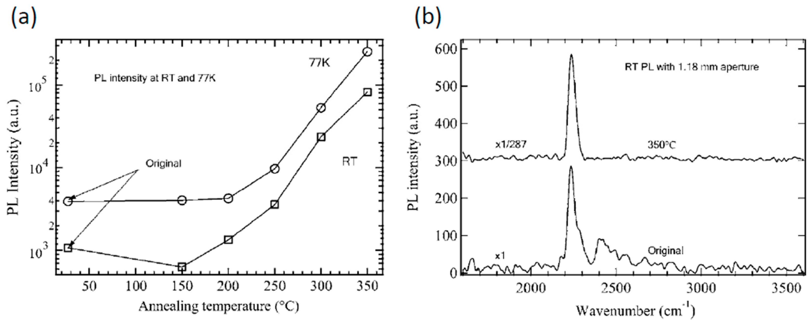
  63. Dashevsky, Z.; Kasiyan, V.; Radovsky, G.; Shufer, E.; Auslender, M. Mid-infrared photoluminescence of PbSe film structures up to room temperature. In Proceedings of the Sixth International Conference on Advanced Optical Materials and Devices (Aomd-6), Riga, Latvia, 24–27 August 2008. [Google Scholar]
  64. Yang, H.; Chen, L.; Zheng, J.B.; Qiao, K.; Li, X.J. Influence of as-deposited conductive type on sensitization process of PbSe films. Appl. Phys. A Mater. 2016, 122, 710. [Google Scholar] [CrossRef]
  65. Ubrig, N.; Jo, S.; Berger, H.; Morpurgo, A.F.; Kuzmenko, A.B. Scanning photocurrent microscopy reveals electron-hole asymmetry in ionic liquid-gated WS2 transistors. Appl. Phys. Lett. 2014, 104, 171112. [Google Scholar] [CrossRef] [Green Version]
  66. Liu, C.H.; Chang, Y.C.; Norris, T.B.; Zhong, Z.H. Graphene photodetectors with ultra-broadband and high responsivity at room temperature. Nat. Nanotechnol. 2014, 9, 273–278. [Google Scholar] [CrossRef] [PubMed]
  67. Zhao, F.; Mukherjee, S.; Ma, J.; Li, D.; Elizondo, S.L.; Shi, Z. Influence of oxygen passivation on optical properties of PbSe thin films. Appl. Phys. Lett. 2008, 92, 211110. [Google Scholar] [CrossRef]
  68. Golubchenko, N.V.; Moshnikov, V.A.; Chesnokova, D.B. Doping effect on the kinetics and mechanism of thermal oxidation of polycrystalline PbSe layers. Inorg. Mater. 2006, 42, 942–950. [Google Scholar] [CrossRef]
  69. Kastek, M.; Piatkowski, T.; Polakowski, H.; Barela, J.; Firmanty, K.; Trzaskawka, P.; Vergara, G.; Linares, R.; Gutierrez, R.; Fernandez, C.; et al. Technology of uncooled fast polycrystalline PbSe focal plane arrays in systems for muzzle flash detection. Proc. SPIE 2014, 9074. [Google Scholar]
  70. Vergara, G.; Gomez, L.J.; Villamayor, V.; Alvarez, M.; Torquemada, M.C.; Rodrigo, M.T.; Verdu, M.; Sanchez, F.J.; Almazan, R.M.; Plaza, J.; et al. Monolithic uncooled IR detectors of polycrystalline PbSe: A real alternative-art. Proc. SPIE 2007, 6542, 654220. [Google Scholar]
  71. Sanchez, F.J.; Rodrigo, M.T.; Vergara, G.; Lozano, M.; Santander, J.; Torquemada, M.C.; Gomez, L.J.; Villamayor, V.; Alvarez, M.; Verdu, M.; et al. Progress on monolithic integration of cheap IR FPAs of polycrystalline PbSe. Proc. SPIE 2005, 5783, 441–447. [Google Scholar]
  72. Vergara, G.; Montojo, M.T.; Torquemada, M.C.; Rodrigo, M.T.; Sanchez, F.J.; Gomez, L.J.; Almazan, R.M.; Verdu, M.; Rodriguez, P.; Villamayor, V.; et al. Polycrystalline lead selenide: The resurgence of an old infrared detector. Opto-Electron. Rev. 2007, 15, 110–117. [Google Scholar] [CrossRef]
  73. Torquemada, M.C.; Rodrigo, M.T.; Vergara, G.; Sanchez, F.J.; Almazan, R.; Verdu, M.; Rodriguez, P.; Villamayor, V.; Gomez, L.J.; Montojo, M.T.; et al. Role of halogens in the mechanism of sensitization of uncooled PbSe infrared photodetectors. J. Appl. Phys. 2003, 93, 1778–1784. [Google Scholar] [CrossRef]
  74. Diezhandino, J.; Vergara, G.; Perez, G.; Genova, I.; Rodrigo, M.T.; Sanchez, F.J.; Torquemada, M.C.; Villamayor, V.; Plaza, J.; Catalan, I.; et al. Monolithic integration of spectrally selective uncooled lead selenide detectors for low cost applications. Appl. Phys. Lett. 2003, 83, 2751–2753. [Google Scholar] [CrossRef]
  75. Qiu, J.J.; Weng, B.B.; Yuan, Z.J.; Shi, Z.S. Study of sensitization process on mid-infrared uncooled PbSe photoconductive detectors leads to high detectivity. J. Appl. Phys. 2013, 113, 103102. [Google Scholar] [CrossRef]
  76. Weng, B.B.; Qiu, J.J.; Zhao, L.H.; Yuan, Z.J.; Chang, C.; Shi, Z.S. Recent development on the uncooled mid-infrared PbSe detectors with high detectivity. Proc. SPIE 2014, 8993, 899311. [Google Scholar]
  77. Yang, H.; Chen, L.; Li, X.J.; Zheng, J.B. Intrinsic stoichiometry optimization of polycrystalline lead selenide film in the sensitization process by iodine concentration regulation. Mater. Lett. 2016, 169, 273–277. [Google Scholar] [CrossRef]
  78. Kumar, P.; Pfeffer, M.; Schweda, E.; Eibl, O.; Qiu, J.J.; Shi, Z.S. PbSe mid-IR photoconductive thin films (part I): Phase analysis of the functional layer. J. Alloy. Compd. 2017, 724, 316–326. [Google Scholar] [CrossRef]
  79. Peranio, N.; Eibl, O. Quantitative EDX microanalysis of Bi2Te3 in the TEM. Phys. Status Solidi A 2007, 204, 3243–3255. [Google Scholar] [CrossRef]
  80. Virt, I.S.; Rudyi, I.O.; Lopatynskyi, I.Y.; Dubov, Y.; Tur, Y.; Lusakowska, E.; Luka, G. Growth Mechanisms and Structural Properties of Lead Chalcogenide Films Grown by Pulsed Laser Deposition. J. Electron. Mater. 2017, 46, 175–181. [Google Scholar] [CrossRef]
  81. Kumar, P.; Pfeffer, M.; Berthold, C.; Eibl, O. PbSe mid-IR photoconductive thin films (part-II): Structural analysis of the functional layer. J. Alloy. Compd. 2018, 735, 1654–1661. [Google Scholar] [CrossRef]
  82. Kumar, P.; Pfeffer, M.; Peranio, N.; Eibl, O.; Bassler, S.; Reith, H.; Nielsch, K. Ternary, single-crystalline Bi2 (Te, Se)3 nanowires grown by electrodeposition. Acta Mater. 2017, 125, 238–245. [Google Scholar] [CrossRef]
  83. Weng, B.B.; Qiu, J.J.; Yuan, Z.J.; Larson, P.R.; Strout, G.W.; Shi, Z.S. Responsivity enhancement of mid-infrared PbSe detectors using CaF2 nano-structured antireflective coatings. Appl. Phys. Lett. 2014, 104, 021109. [Google Scholar] [CrossRef]
  84. Retherford, R.S.; Sabia, R.; Sokira, V.P. Effect of surface quality on transmission performance for (111) CaF2. Appl Surf. Sci. 2001, 183, 264–269. [Google Scholar] [CrossRef]
  85. Brunner, R.; Sandfuchs, O.; Pacholski, C.; Morhard, C.; Spatz, J. Lessons from nature: Biomimetic subwavelength structures for high-performance optics. Laser Photonics Rev. 2012, 6, 641–659. [Google Scholar] [CrossRef]
  86. Chang, C.H.; Dominguez-Gaballero, J.A.; Choi, H.J.; Barbastathis, G. Nanostructured gradient-index antireflection diffractive optics. Opt. Lett. 2011, 36, 2354–2356. [Google Scholar] [CrossRef] [PubMed]
  87. Linn, N.C.; Sun, C.H.; Jiang, P.; Jiang, B. Self-assembled biomimetic antireflection coatings. Appl. Phys. Lett. 2007, 91, 101108. [Google Scholar] [CrossRef]
  88. Park, K.C.; Choi, H.J.; Chang, C.H.; Cohen, R.E.; McKinley, G.H.; Barbastathis, G. Nanotextured Silica Surfaces with Robust Superhydrophobicity and Omnidirectional Broadband Supertransmissivity. ACS Nano 2012, 6, 3789–3799. [Google Scholar] [CrossRef] [PubMed]
  89. Kuo, M.L.; Poxson, D.J.; Kim, Y.S.; Mont, F.W.; Kim, L.K.; Schuhert, E.F.; Lin, S.Y. Realization of a near-perfect antireflection coating for silicon solar energy utilization. Opt. Lett. 2008, 33, 2527–2529. [Google Scholar] [CrossRef] [PubMed]
  90. Hill, D.M.; Meyer, H.M.; Weaver, J.H.; Nelson, D.L. Passivation of High-Tc Superconductor Surfaces with CaF2 and Bi, Al, and Si Oxides. Appl. Phys. Lett. 1988, 53, 1657–1659. [Google Scholar] [CrossRef]
  91. Mukherjee, S.; Li, D.; Bi, G.; Ma, J.; Elizondo, S.L.; Gautam, A.; Shi, Z. CaF2 surface passivation of lead selenide grown on BaF2. Microelectron. Eng. 2011, 88, 314–317. [Google Scholar] [CrossRef]
  92. Ladany, I.; Zanzucchi, P.J.; Andrews, J.T.; Kane, J.; Depiano, E. Scandium Oxide Antireflection Coatings for Superluminescent Leds. Appl. Opt. 1986, 25, 472–473. [Google Scholar] [CrossRef] [PubMed]
  93. Tsai, D.S.; Lin, C.A.; Lien, W.C.; Chang, H.C.; Wang, Y.L.; He, J.H. Ultra-High-Responsivity Broadband Detection of Si Metal-Semiconductor-Metal Schottky Photodetectors Improved by ZnO Nanorod Arrays. ACS Nano 2011, 5, 7748–7753. [Google Scholar] [CrossRef] [PubMed]
  94. Kowall, J.; Peak, D.; Corbett, J.W. Impurity-Concentration Profile for an Exponentially Decaying Diffusion-Coefficient in Irradiation Enhanced Diffusion. Phys. Rev. B 1976, 13, 477–478. [Google Scholar] [CrossRef]
  95. Willems, G.J.; Maes, H.E. Analytical Model for the out-Diffusion of an Exponentially Decaying Impurity Profile-Application to Nitrogen in Silicon. J. Appl. Phys. 1993, 73, 3256–3260. [Google Scholar] [CrossRef]
  96. Armstrong, D.E.J.; Edmondson, P.D.; Roberts, S.G. Effects of sequential tungsten and helium ion implantation on nano-indentation hardness of tungsten. Appl. Phys. Lett. 2013, 102, 251901. [Google Scholar] [CrossRef]
  97. Battiato, A.; Bosia, F.; Ferrari, S.; Olivero, P.; Sytchkova, A.; Vittone, E. Spectroscopic measurement of the refractive index of ion-implanted diamond. Opt. Lett. 2012, 37, 671–673. [Google Scholar] [CrossRef] [PubMed]
  98. Katsidis, C.C. Refractive index, free carrier concentration, and mobility depth profiles of ion implanted Si: Optical investigation using FTIR spectroscopy. J. Opt. Soc. Am. B 2008, 25, 854–864. [Google Scholar] [CrossRef]
  99. Kepaptsoglou, D.; Hardcastle, T.P.; Seabourne, C.R.; Bangert, U.; Zan, R.; Amani, J.A.; Hofsass, H.; Nicholls, R.J.; Brydson, R.M.D.; Scott, A.J.; et al. Electronic Structure Modification of Ion Implanted Graphene: The Spectroscopic Signatures of p- and n-Type Doping. ACS Nano 2015, 9, 11398–11407. [Google Scholar] [CrossRef] [Green Version]
  100. Yang, H.; Li, X.J.; Mei, T.; Zheng, J.B. Deep inherent sensitization of lead selenide material via an effective oxygen ion preparation method. Mater. Lett. 2017, 194, 142–144. [Google Scholar] [CrossRef]
  101. Yang, H.; Li, X.J.; Mei, T.; Zheng, J.B. The lead selenide photoconductive sensitization via oxygen ion implantation with enhanced optical absorption and carrier mobility. J. Mater. Sci. 2017, 52, 10779–10786. [Google Scholar] [CrossRef]
  102. De Wolf, S.; Holovsky, J.; Moon, S.J.; Loper, P.; Niesen, B.; Ledinsky, M.; Haug, F.J.; Yum, J.H.; Ballif, C. Organometallic Halide Perovskites: Sharp Optical Absorption Edge and Its Relation to Photovoltaic Performance. J. Phys. Chem. Lett. 2014, 5, 1035–1039. [Google Scholar] [CrossRef]
  103. Cody, G.D.; Tiedje, T.; Abeles, B.; Brooks, B.; Goldstein, Y. Disorder and the Optical-Absorption Edge of Hydrogenated Amorphous-Silicon. Phys. Rev. Lett. 1981, 47, 1480–1483. [Google Scholar] [CrossRef]
  104. Sun, X.G.; Gao, K.W.; Pang, X.L.; Yang, H.S.; Volinsky, A.A. Structure and composition effects on electrical and optical properties of sputtered PbSe thin films. Thin Solid Films 2015, 592, 59–68. [Google Scholar] [CrossRef]
  105. Song, Q.C.; Zhou, J.W.; Meroueh, L.; Broido, D.; Ren, Z.F.; Chen, G. The effect of shallow vs. deep level doping on the performance of thermoelectric materials. Appl. Phys. Lett. 2016, 109, 263902. [Google Scholar] [CrossRef] [Green Version]
  106. Yoon, Y.; Yan, Y.X.; Ostrom, N.P.; Kim, J.; Rozgonyi, G. Deep level transient spectroscopy and minority carrier lifetime study on Ga-doped continuous Czochralski silicon. Appl. Phys. Lett. 2012, 101, 222107. [Google Scholar] [CrossRef]
  107. Chen, G.; Hoang, A.M.; Bogdanov, S.; Haddadi, A.; Bijjam, P.R.; Nguyen, B.M.; Razeghi, M. Investigation of impurities in type-II InAs/GaSb superlattices via capacitance-voltage measurement. Appl. Phys. Lett. 2013, 103, 033512. [Google Scholar] [CrossRef]
Figure 1. Various potential applications for uncooled photodetector with lead selenide (PbSe) polycrystalline coating in mid-infrared range. Reprinted with permission from [49]. Copyright SPIE 2013.
Coatings 08 00444 g001
Figure 2. The schematics of (a) the minority carrier trap and (b) the grain boundary barrier models.
Coatings 08 00444 g002
Figure 3. The schematic of the charge separation model, showing (a) the conversion of crystallites’ surfaces from p- to n-type, (b) the charge carrier transport, and (c) the crystallite structure. Reprinted with permission from [62]. Copyright AIP 2014.
Coatings 08 00444 g003
Figure 4. The defect passivation effect on the PbSe thin films fabricated by molecular beam epitaxy (MBE), (a) photoluminescence (PL) intensities versus annealing temperature at room temperature and 77 K, (b) a comparison of PL intensities of PbSe thin films treated at 350 °C and an as-grown one at room temperature. Reprinted with permission from [67]. Copyright AIP 2008.
Coatings 08 00444 g004
Figure 5. (a) A schematic of charge separation under mid-infrared (IR) illumination and (b) the corresponding energy diagram in the sensitized PbSe polycrystalline coatings based on electrical conductive type effect, (c) the X-ray diffraction (XRD) patterns of n-type and p-type PbSe thin fims. Reprinted with permission from [64]. Copyright Springer 2016.
Coatings 08 00444 g005
Figure 6. The (a) morphological, (b) structural, and (c) photoluminescence (PL) optical properties of PbSe polycrystalline coatings fabricated by annealing in single or hybrid atmosphere, and (d) the PL intensity as a function of crystallite size. Reprinted with permission from [75]. Copyright AIP 2013.
Coatings 08 00444 g006
Figure 7. (a) Schematic of I–V tests under mid-IR illumination, (b) I–V test results for iodine concentration of 9.1 × 1011 mm−3, (c) scanning electron microscopy (SEM) morphologies for as-grown and iodized samples using different iodine concentrations, (d) the responsivity, (e) Pb/Se and I/O atomic ratios, and (f) the atomic proportions versus iodine concentration. Reprinted with permission from [77]. Copyright Elsevier 2016.
Coatings 08 00444 g007
Figure 8. The cross-section structure of PbSe polycrystalline coating sensitized in an oxygen/iodine hybrid atmosphere, (a) a schematic, (b) nanocrystalline phase, and (c) polycrystalline phase. Reprinted with permission from [78]. Copyright Elsevier 2017.
Coatings 08 00444 g008
Figure 9. Selected area electron diffraction patterns (SAED) patterns, energy-dispersive X-ray spectroscopy (EDX) spectra, and electron energy-loss spectroscopy (EELS) spectra of (a) PbSe bottom layer, (b) a nanocrystalline phase of the top layer with the largest d spacing of 0.892 nm, and (c) a polycrystalline phase of the top layer with the largest d spacing of 1.069 nm. Reprinted with permission from [78]. Copyright Elsevier 2017.
Coatings 08 00444 g009
Figure 10. (a) Energy-filtered selected area diffraction patterns in the [100], [010], and [111] poles, and the corresponding schematics of the pseudo-orthorhombic crystal structure of the iodized PbSe polycrystalline coatings; (b) the high-resolution transmission electron microscopy (HRTEM) images along the c-axis; (c) low-loss electron energy-loss spectroscopy (EELS) spectra for distinguishing the PbSexIyOz phase from PbSe. Reprinted with permission from [81]. Copyright Elsevier 2017.
Coatings 08 00444 g010
Figure 11. The morphological and optical properties of CaF2 nanostructure-coated PbSe polycrystalline film; (a) high-resolution field emission scanning electron microcopy (FESEM) image of CaF2 nanostructure arrays; (b) cross-sectional FESEM image; and (c) magnified view of PbSe polycrystalline film with CaF2 nanostructured coating; (d) schematics of light bending effect and gradient refractive index profile of CaF2 nanostructured coating. Reprinted with permission from [83]. Copyright AIP 2014.
Coatings 08 00444 g011
Figure 12. Comparisons of the (a) responsivity; (b) reflectance; and (c) PL spectra of PbSe polycrystalline film with and without CaF2 nanostructured coating. Reprinted with permission from [83]. Copyright AIP 2014.
Coatings 08 00444 g012
Figure 13. Preparations and characterizations of PbSe polycrystalline coatings prepared by oxygen ion beam implantation: (a) morphological and structural; (b) Tauc’s plot; (c) Urbach tail; and (d) responsivity spectra with a comparison with the diffused one. Reprinted with permission from [100]. Copyright Elsevier 2017.
Coatings 08 00444 g013aCoatings 08 00444 g013b
Figure 14. Schematics of (a) preparation and (b) photosensitivity mechanism; the (c) morphological, (d) structural, (e) optical, and (f) electrical properties; (gi) the optoelectronic characterizations. Reprinted with permission from [101]. Copyright Springer 2017.
Coatings 08 00444 g014
Figure 15. The summaries and comparisons of different sensitization methods.
Coatings 08 00444 g015

