Article

Enhancement for Potential-Induced Degradation Resistance of Crystalline Silicon Solar Cells via Anti-Reflection Coating by Industrial PECVD Methods

1
Institute of Photonic System, National Chiao Tung University, Tainan 71150, Taiwan
2
E-ton Solar Tech Co., Ltd., Tainan City 709, Taiwan
3
Department of Materials Science and Engineering, National Dong Hwa University, Hualien 97401, Taiwan
*
Authors to whom correspondence should be addressed.
Coatings 2018, 8(12), 418; https://doi.org/10.3390/coatings8120418
Submission received: 7 October 2018 / Revised: 3 November 2018 / Accepted: 21 November 2018 / Published: 22 November 2018
(This article belongs to the Special Issue Advanced Thin Film Materials for Photovoltaic Applications)

Abstract

:
The issue of potential-induced degradation (PID) has gained more concerns due to causing the catastrophic failures in photovoltaic (PV) modules. One of the approaches to diminish PID is to modify the anti-reflection coating (ARC) layer upon the front surface of crystalline silicon solar cells. Here, we focus on the modification of ARC films to realize PID-free step-by-step through three delicate experiments. Firstly, the ARC films deposited by direct plasma enhanced chemical vapor deposition (PECVD) and by indirect PECVD were investigated. The results showed that the efficiency degradation of solar cells by indirect PECVD method is up to −33.82%, which is out of the IEC 62804 standard and is significantly more severe than by the direct PECVD method (−0.82%). Next, the performance of PID-resist for the solar cell via indirect PECVD was improved significantly (PID reduced from −31.82% to −2.79%) by a pre-oxidation step, which not only meets the standard but also has higher throughput than direct PECVD. Lastly, we applied a novel PECVD technology, called the pulsed-plasma (PP) PECVD method, to deal with the PID issue. The results of the HF-etching rate test and FTIR measurement indicated the films deposited by PP PECVD have higher potential against PID in consideration of less oxygen content in this film. That demonstrated the film properties were changed by applied a new control of freedom, i.e., PP method. In addition, the 96 h PID result of the integrated PP method was only −2.07%, which was comparable to that of the integrated traditional CP method. In summary, we proposed three effective or potential approaches to eliminate the PID issue, and all approaches satisfied the IEC 62804 standard of less than 5% power loss in PV modules.

1. Introduction

Photovoltaic (PV) has been recognized as the most competitive renewable energy among various renewable technologies according to its diverse applications and is a candidate of next generation large-volume power plants. For instance, Águas et al. [1] applied the PV for building-integrated photovoltaics (BIPV) application; Águas et al. [2] also fabricated thin film solar cells on cellulose paper for flexible, wearable application; and most of all was for large-scale power plants. According to the statistic reports of International Energy Agency (IEA), it pointed out that the cumulative installed capacity of solar installations was almost 303 GW at the end of 2016 [3]. Based on the demand for long-term and safe operation, the reliabilities of PV modules gain more attention. In Figure 1, we depicted the components of crystalline silicon module under negative bias. Solar cells were held in between the front glass cover and the rear backsheet. The glass was used for light transmission and module protection; the backsheet was implemented for the reflection of incident lights shined at the gap between individual solar cells and for the reflection of residual lights that penetrate the solar cells. In general, the lifetime of PV modules was designed over 25 years. However, several kinds of issues resulted in irreversible degradation of PV modules, in which one of the most catastrophic failures was noted as potential-induced degradation (PID).
PID was firstly reported for both crystalline silicon modules and amorphous silicon thin film modules by the Jet Propulsion Laboratory in 1985, but it was observed by SunPower Corp. until 2005 and coined by Pingel et al. in 2010 [4,5]. PID is ascribed to a high electric potential difference across a PV module inducing a leakage current flowing through the solar cells, which results in reversible or irreversible power conversion efficiency degradation. The schematic diagram is shown in Figure 1. Currently, 1000 V is applied in a PV power system to minimize the electric power transportation loss by serially connected PV modules. Nevertheless, the PID of PV modules is significantly enhanced under a high bias. For p-type Si-based solar cells, the most remarkable type of PID mechanism is “potential induced shunting” (PID-s). PID-s describes a degradation ascribed to both sodium ions and solar cells under a negative-biased condition. Sodium ions (Na+), coming from soda-lime glass, are drifted through the anti-refractive coating (ARC) layer, and then accumulate at the ARC/Si interface or in the stacking faults. Finally, the shunting paths are formed, and then the p-n junction is damaged.
Several promising strategies to approach PID-resistant PV systems have been proposed for cell-, module-, or system-levels [6,7]. On the cell-level, modifying the ARC layer by elevating its refractive index (RI) has well been demonstrated to alleviate the PID-s issue [5,7,8,9,10]. In the factory of c-Si solar cells, various plasma enhanced chemical vapor deposition (PECVD) methods provide the ARC layers for solar cells, including direct, remoter, continuous-plasma (CP) and pulsed-plasma (PP) types. From the literature, it was reported that increasing the RI of the ARC layer improves its electric conductivity which can prevent positive charges accumulating in the surface and Na+ drifted by electric field. However, if the RI of the ARC layer deviates from the theoretically optimal value (i.e., the square-root of the RI of silicon), the light trapping performance of ARC degrades. Hence, there is a trade-off between PID-resistant ability and power conversion efficiency (PCE). In addition, Mishina et al. [11] pointed out that the film quality of the ARC has a great impact on PID-resistant ability. They showed that the ARC films deposited by the novel direct PECVD performed better PID-resistance than the one deposited by remoter PECVD, even without scarifying the PCE (i.e., keeping the conventional RI value). However, direct PECVD, in comparison with remoter PECVD, has relatively low throughput and gains additional running costs in commercialized applications. Beside the modification of ARC films, a thin oxide film between the ARC and Si substrate has been proven as another efficient solution for PID-resistant solar cells [7,12,13]. Furthermore, Nagel et al. demonstrated that the cells with this thin thermal oxide layer gained a 0.2% increase in PCE, which is ascribed to the improvement of surface passivation in the front surface [12].
Recently, a novel PECVD method, PP modulated PECVD, is commonly used for modifying SiNx films by controlling the ion bombardment and film nucleation process [14,15,16,17]. Contrary to continuous-plasma PECVD, the manipulation of pulsed-plasma PECVD is by using a frequency modulated glow discharge during deposition, and then modifying the film qualities. After ionization, the lifetimes between free radicals remain different, and then the clusters during the film synthesization have been designated by controlling the duty cycle and periods. The duty cycle is the ratio of conducting glow discharge to the periods, as shown in the schematic diagram in Figure 2. In the scenario of low frequency modulated radio frequency (RF) discharge (40 Hz) in Watanabe et al.’s study [18], lifetimes of SiHn (n = 0–2) radicals were shorter than 10 ms (these were estimated to be below 3 ms); whereas the lifetime of SiH3 was longer than 20 ms. Regarding the achievement of film quality modification by PP PECVD, Watanabe et al. also pointed out the film mainly composed of SiH3 shows fewer dangling bonds and reduced powder particle in size during deposition [18]. In addition, Viera et al. reported a high purity and controllable nanostructure achieved by the PP method [19], and Byungwhan Kim et al. pointed out that the films made by the PP method present denser and smoother surface roughness [20].
The PID issue has been addressed for years. Current PV power plants have enrolled different kinds of cutting edge technologies to solve uprising PID concern. For instance, other types of solar cells (PERC and HIT) with inherent high voltage output are becoming mainstream, and 1500 V power system are replacing traditional 1000 V power systems [10,21]. In consideration of even stricter PID-resistant demands, improved or novel PID-resistant solutions are necessary in the future. In this work, we firstly proposed a PP PECVD technology to deal with the PID issue. Besides, the comparisons of the ARC films deposited by direct and indirect PECVD, and the enhancement of the PID-resistant ability by the additional interface oxide layer were investigated.

2. Materials and Methods

In this work, three closely related experiments were designed to approach PID-free c-Si solar cells. The cell structure is depicted in Figure 1. First, we compared PID-resistant abilities between different kinds of commercially available PECVD, namely direct PECVD (Shimadzu Corporation, Kyoto, Japan) and indirect PECVD (OTB SOLAR DEPX 2400). For the direct PECVD system, the electrodes are placed across the specimens, and the reactant gases are ionized nearby the specimens. Besides, the electric field across the electrodes can boost the moment of ions and thus these energetic ions bombard the deposited film during deposition. Contrary to direct PECVD, the gaseous ions are generated separately from the substrates and sent to target locations through an inlet for the indirect PECVD. Secondly, in consideration of the relatively higher throughput of the OTB system, we introduced a thin oxide layer at the interface of the ARC film and Si to solve the PID issue. For these two experiments, we used 6-inch multi-crystalline silicon (mc-Si) solar cells with traditional Al back surface field (BSF), and these specimens were tested by the standard PID testing procedure. Moreover, we investigated the SiNx films deposited by PP and CP PECVD (Otb Solar Depx 2400 by Roth & Rau, Hohenstein-Ernstthal, Germany). In common, there are two approaches to modulate the glow discharge for realizing the PP method by either controlled inlet gas or controlled bias. The latter one was employed in this work. The deposition parameters of RF frequency, modulated frequency, and duty cycle are 13.56 MHz, 80 Hz and 50%, respectively. For the PID test, we replaced the conventional mc-Si solar cells by the PERC-type mono-crystalline silicon (c-Si) solar cells which had a thin oxide layer located at the interface of the ARC and Si as well. For the characterizations of these films, we also conducted a dilute HF etching test. The dilute HF-etching rate has been pointed out as a good indicator of the film quality against PID [11]. A total of eight specimens with an RI value of 2.06 deposited by the CP and PP method were dipped in 3.85 vol % HF solution at room temperature. Fourier transform infrared (FTIR) spectra were conducted for the chemical composition of SiNx films.
Based on the instruction of standard reliability test of PID, IEC-62804-1 [22], we followed and even tested a more severe testing condition to clarify the significance of experimental variables. All specimens in this experiment were carried out by the same PID testing procedures as following:
(1)
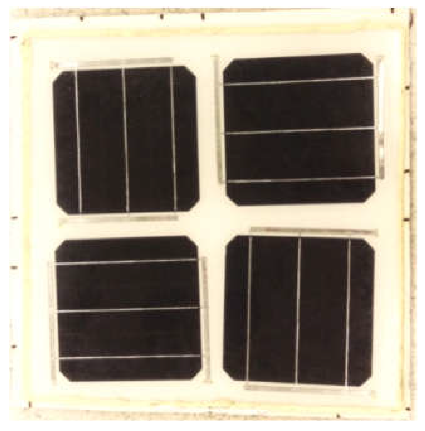
Four solar cells were laminated in one module but disconnected from each other as shown in Figure 3.
(2)
The electric performances and electroluminescence (EL) images of the PV modules were recorded before PID testing.
(3)
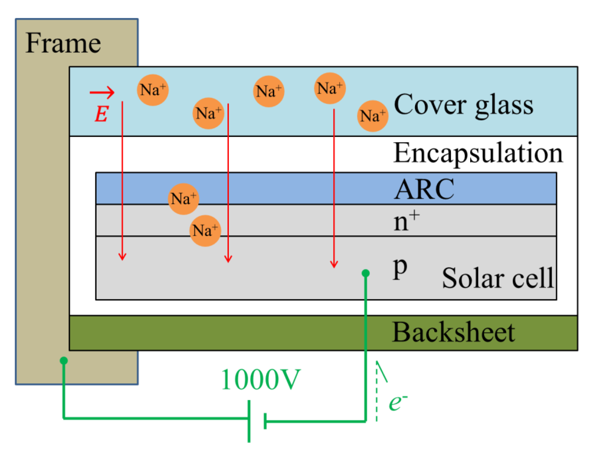
Aluminum foils with deionized water wetted were attached upon the front glasses of modules, and then connected with the positive terminal of a high-voltage power source.
(4)
On the other hand, the negative terminal of this high-voltage power source was connected to the shunted cathodes and anodes of solar cells.
(5)
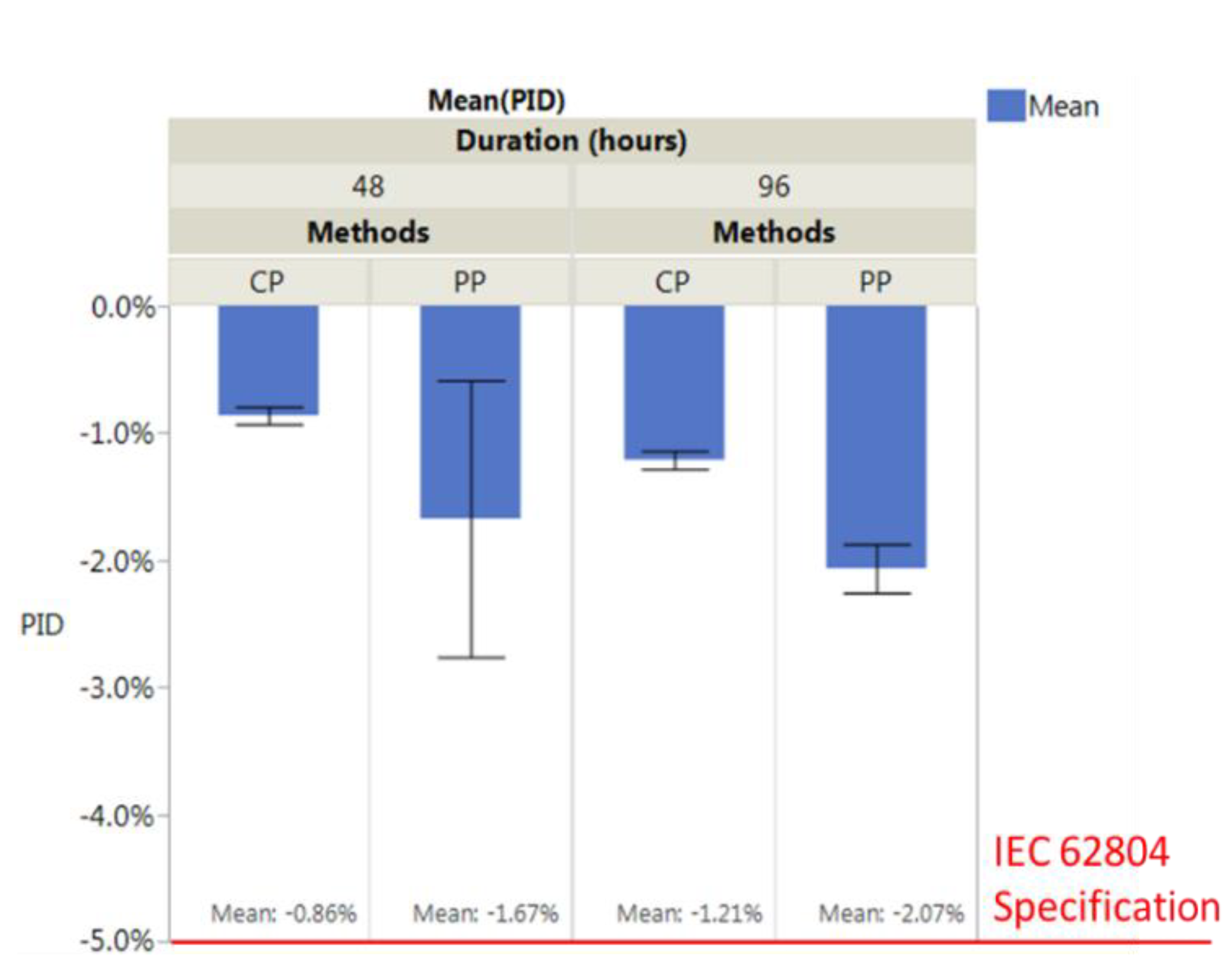
PV modules were processed in a climate chamber for 48/96 h, at 85 °C, with 85% relative humidity, and −1000 V bias.
(6)
After PID treatment, the measurements referred to in Step 2 were repeated.
The equation for characterizing PID is listed as Equation (1):
PID   ( % ) = ( P m p p , A F P m p p , B F ) P m p p , B F
where Pmpp,AF is the maximum output power under standard testing conditions after PID treatment, and Pmpp,BF is the one before PID treatment. Under the IEC 62804 standard, modules with less than 5% power loss and without induced major defects could be recognized as PID resistance [23,24].

3. Results and Discussion

3.1. PID-Resistant Approach via Film-Quality Modification

The PID-resistance of two film deposition methods was compared in this experiment, i.e., direct and indirect PECVD. The detail comparison of our equipment of these two approaches and the corresponding results are listed in Table 1. After performing the PID test, the results for mc-Si solar cells with SiNx films deposited by the direct and indirect PECVD are presented in Table 2, showing the EL images before and after the PID test and power conversion efficiency loss. For the EL images, before PID treatment, both kinds of cells perform uniform illumination under forward bias. The EL image of the cells via indirect PECVD is relatively less uniform than via direct PECVD, which is ascribed to the inherent less gas inlets in indirect PECVD equipment. After the PID test, the apparent dark areas (marked by a red oval) were observed for the EL image of the cells via indirect PECVD, but barely seen for the direct PECVD. It indicates the more severe power conversion efficiency loss for the cell via indirect PECVD. The power conversion efficiency loss of the cell via the indirect PECVD method is up to −33.82%, significantly more severe than the one via the direct PECVD method (−0.82%). The highlighted areas in the red circles in Table 2 are located between two bus bars. This phenomenon can be interpreted by the PID-shunt model [7], where Na+ ions are firstly accumulated on the surface of the ARC driven by the applied negative bias, and are then drifted through the ARC layer, and finally shunt the p-n junction dramatically.
Comparing the two deposition methods, the SiNx films deposited by direct PECVD are denser, more compact, and more conformal, but had more surface damages due to ions bombardment. Therefore, we deduce that the denser SiNx film made by direct PECVD can resist Na+ penetration due to less pin holes and smaller clusters during deposition. However, its lower productivity is a concern from the point-of-view of industrial applications [11,16,25,26].

3.2. PID-Resistant Approach via Pre-Oxidation Treatment

Although Si solar cells via indirect PECVD is associated with severe PID concern, we note the advantages of ultrahigh deposition rate (5 nm/s), which has high throughput for mass production [26]. A pre-oxidation step before ARC films by indirect PECVD was introduced to improve PID-resistance ability. Therefore, a thin oxide layer (SiO2 or SiOxNy) was formed between ARC and Si substrate by using a furnace with an atmosphere of O2 and N2 and with the setting temperature of 800 °C. The thickness of this oxide layer was around 2 to 5 nm confirmed by ellipsometer. In this section, the specimens with and without this interface oxide layer were produced. The PID testing results are presented in Table 3. The PID effect was dramatically improved and was down to −2.79% by inserting an oxide layer, which well fulfills the IEC 62804 standard of power loss less than −5%. The root cause about the role of the oxide layer was explained by Naumann et al. [27], and the extensive research about the role of oxide layer in the recovery process of PID was reported by Lausch et al. [28]. Volker Naumann pointed out two facts by investigating the cross section of the solar cell after PID treatment by TEM and EDX mapping. (1) Na was accumulated at the c-Si stacking fault resulting in the creation of a shunting path. (2) The results of O mapping identified the position of the interface oxide layer, and, moreover, the Na was also “trapped” and scatteringly distributed in the oxide layer. Lausch et al. further proved that this oxide layer may assist the Na to diffuse out from c-Si stacking fault when performing a PID recover experiment. In addition, the oxide layer served as a barrier against Na drift into the silicon base. In short, the PID-resistant ability can be improved by a factor of 10 in this experiment by introducing a thin oxide layer between Si and SiNx films in the case of indirect PECVD which can fit the high-throughput requirement of the fabrication of Si solar cells.

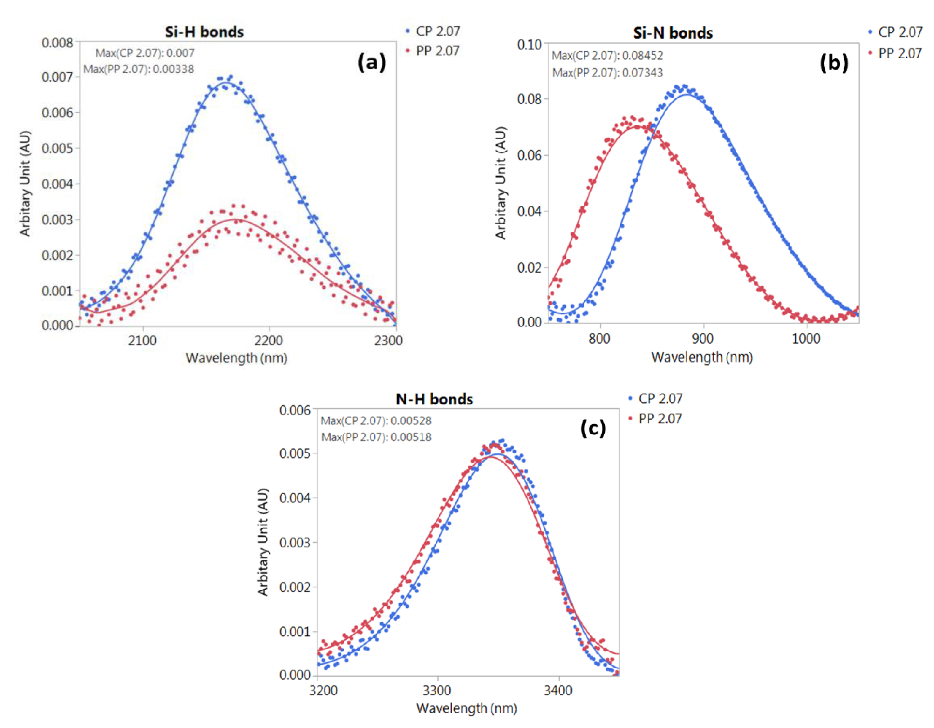
3.3. A Novel PID-Resistant Approach via SiNx Film Deposited by PP PECVD

Recently, PP PECVD is becoming the mainstream technique for the fabrication of c-Si solar cells. This novel method has some remarkable advantages, including higher throughput, no additional process step, being easier to control the film quality, and so on. Hence, we firstly proposed a novel study to improve the PID-resistance of SiNx films by PP PECVD. In addition, regarding higher PID-resistant demands for modern solar cells, we evaluated the PID-resistance of 6-inch c-Si PERC-type solar cells. For the characterization of these films, we conducted a dilute HF etching test, FTIR measurement, and PID test for SiNx films deposited by CP and PP methods.
The etched film thickness for different etching duration is presented in Figure 4. The film thicknesses of origin, and after 3, 6, and 9 min etched, were measured by ellipsometer, and the discrepancies were calculated. The HF-etching rates were deduced by linear fitting. The HF-etching rate of SiNx film deposited by PP PECVD is 2.5 nm/min, 2.6 times lower than the one by CP PECVD. Mishina et al. [11] pointed out that the mechanism of HF etching is associated with the SiNx dissociations via oxygen assistance, i.e., higher oxygen density in the SiNx film leads to a larger HF-etching rate. In addition, the SiNx film with lower HF etching rate (lower oxygen density) is related to high PID-resistance [11]. The root cause is that the oxygen contained in SiNx may be in the form of SiN2O or SiO2, and subsequently, the SiO2 dissolved in the molten salt (Na+) will form a liquid sodium silicate (Na2O·(SiO2)) [11,29,30]. The oxygen-assisted corrosion of the SiNx film in molten salt would create a shunting path and then worsens the original PID-resistance of the ARC film. Accordingly, since our ARC films made by the PP method contain less oxygen atoms than by the CP method, we derived the SiNx film bade by the PP method to perform better PID-resistance.
FTIR measurement was employed to characterize the chemical composition discrepancies between the films deposited by CP and by PP methods, and the results are shown in Figure 5. The absorbance at 850 cm−1 was designated as the asymmetric stretching vibration mode of Si–N bonding [31]; the absorbance at 2160 cm−1 was designated as the in phase stretching vibration mode of Si-rich Si–H bonds [32]. Compared to the peak of Si–N stretching mode of the SiNx film deposited by the PP method located at 831.2 cm−1, the one deposited by the CP method is at 881 cm−1. Shinichi Kobayashi reported that the large blue shift of the Si–N stretching mode is ascribed to oxidation because of the net change of electronegativity around the Si–N bonds due to the increase in the Si–O bond density [33]. The blue-shifted peak of Si–N mode indicates that the CP method-deposited SiNx film contains inherently higher oxygen, which agrees with the result of the dilute HF etching test. These results also suggest that the PP method can diminish the oxygen content in SiNx as well as can increase the PID-resistant ability. The absorbance peak at 3350 cm−1 is designated as N–H bonds [34], and these N–H bonds present almost identical for the films deposited both PP and CP methods. In addition, Si–N and Si–H peak magnitudes of the PP method-deposited SiNx film are significantly less than that of the CP method-deposited SiNx film. These results indicate that our PP method-deposited SiNx film is either relatively thinner or has a smaller RI value (or less Si content) than that of the CP method-deposited one. Ideally, to compare the PID-resistant ability of SiNx films deposited by CP and PP methods, it should have the same thickness and Si content. Therefore, these observed either thinner or lower Si content films might lead us under evaluate the anti-PID ability of the PP method SiNx film because Na+ can easier penetrate into thinner and accumulate on lower conductivity SiNx films. Nevertheless, we succeeded in the modification of the SiNx property of film thickness, silicon content, or oxygen content by introducing the PP method as an additional control of freedom.
Finally, not only the 48- but also 96-h PID treatments for c-Si PERC-type solar cells, in which there were four and two pieces respectively, were performed and are shown in Figure 6. Simultaneously, EL images are shown in Table 4. PID results revealed that both groups of samples fit the requirement of IEC 62804 specification, i.e., power conversion efficiency loss of the cells after PID test is under 5%. It was noticeable that the PP group for 48-h testing had shown the largest error bar. This is because we retained all data and one of them seemed to be an outlier (−1.07%, −1.09%, −1.23%, −3.30%). As the duration of PID test increases, the power conversion efficiency loss gets higher.
The PID-resistant ability of the PP group was slightly lower than the one of the CP group. Since the oxide layer between the ARC film and Si plays an important role in the resistance of PID, the weighting of the PID-resistance ability via the PP modulated PECVD is reduced. Another reason is that the realistic deposition condition of the PP modulated PECVD is slightly away from our expectation. We thought that we had controlled the same RI value (2.07) for both groups and controlled comparable film thicknesses (of 78.6 nm (CP) and 77.9 nm (PP) by single wavelength ellipsometer at 632.8 nm). However, by taking an empirical relation of refractive index with the stoichiometry from Dauwe [35] or complemented to low-pressure PECVD from Lelièvre et al. as below [36]:
n = 1.22 + 0.61 [ Si ] [ N ]
The empirical RI can be estimated through chemical stoichiometry of Si and N. Hence, according to our FTIR results, the film deposited by PP PECVD contains a lower Si concentration, and thus has a lower RI value than the CP method-deposited SiNx film. Therefore, the extracted RI value by single wavelength ellipsometer might not be that accurate, and influences this delicate experiment at the beginning.
To the best of our knowledge, we may be the first team studying PID-resistant ability through the pulsed-plasma indirect PECVD method. This additional control of freedom was realized in adjusting film properties, which was confirmed by the mentioned dilute HF etching test and FTIR measurement. The PID results of the PP method are qualified for the generalized criteria of less than −5%, and has potentially achieved lower power loss if fine-tuning the SiNx film towards a higher RI value. In summary, we demonstrated the ARC of solar cells deposited by the PP method has advantages for higher PID demands.

4. Conclusions

The comparison of PID-resistance for the SiNx films deposited by the direct and indirect PECVD was evaluated. After the PID test, the power conversion efficiency loss of the cell via indirect PECVD method was −33.82%, however, the loss of the cell via direct PECVD method was only −0.82%. Direct PECVD provides dense SiNx films for increasing the PID-resistant ability. By taking the main advantage of the extremely high throughput of inline-type indirect PECVD, we demonstrated that the anti-PID ability can be much improved from −31.82% to −2.79% by introducing a thin oxide layer between indirect PECVD-deposited SiNx film and Si through a simple pre-oxidation step. The oxide layer prevents sodium ions from accumulating at the silicon stacking faults and diminishes the possible shunting path.
Regarding to the uprising PID concern, we introduced a novel PP PECVD method for ARC deposition on PERC-type solar cells. The films made by the PP PECVD method were investigated by dilute HF etching and FTIR, and the corresponding cells were tested by PID treatments. The HF-etching rate of PP deposited SiNx film is 2.5 nm/min, which is 2.6 times lower than that of CP deposited SiNx film. A lower HF-etching rate indicates that the films made by the PP method contain less oxygen atoms and prevent chemical decomposition ascribed to oxidation of Na. The FTIR results consistently showed the lower oxygen content of the PP deposited SiNx film and revealed that the PP deposited SiNx films are thinner or have a smaller refractive index if compared to the CP deposited ones. As a result, we demonstrated the PID results of the cells with PP deposited SiNx film were comparable to the ones with CP deposited SiNx film, and the degradations of all cells satisfied the general criteria of the IEC 62804 specification. In addition, the involvement of pulsed plasma exhibits an extra degree of freedom to tune the film properties. Moreover, we expect the PP deposited SiNx films, with further optimal film thickness and RI, would perform more aggressive PID-resistance than the conventional CP deposited ones.

Author Contributions

Conceptualization, C.-H.K.; Methodology and Data Curation, T.-W.K. and Y.-L.L.; Writing-Original Draft Preparation, T.-C.C.; Writing-Review & Editing, Z.-P.Y. and I.-S.Y.

Funding

This research was funded by Taiwan Ministry of Science and Technology, grant number MOST 106 2221-E-009-199 and MOST 107-2221-E-259-001-MY2.

Acknowledgments

The authors would like to thank the financial support from Ministry of Science and Technology, Taiwan. We also thank E-Ton Solar Tech. for the fabrication of Si solar cells and modules.

Conflicts of Interest

The authors declare no conflict of interest.

References

  1. Águas, H.; Ram, S.K.; Araújo, A.; Gaspar, D.; Vicente, A.; Filonovich, S.A.; Fortunato, E.; Martins, R.; Ferreira, I. Silicon thin film solar cells on commercial tiles. Energy Environ. Sci. 2011, 4, 4620–4632. [Google Scholar] [CrossRef]
  2. Águas, H.; Mateus, T.; Vicente, A.; Gaspar, D.; Mendes, M.J.; Schmidt, W.A.; Pereira, L.; Fortunato, E.; Martins, R. Thin film silicon photovoltaic cells on paper for flexible indoor applications. Adv. Funct. Mater. 2015, 25, 3592–3598. [Google Scholar] [CrossRef]
  3. Masson, G.; Kaizuka, L. Trends 2017 in Photovoltaic Applications; IEA PVPS T1-32:2017; International Energy Agency (IEA): Paris, France, 2017. [Google Scholar]
  4. Swanson, R.; Cudzinovic, M.; DeCeuster, D.; Desai, V.; Jürgens, J.; Kaminar, N.; Mulligan, W.; Rodrigues-Barbarosa, L.; Rose, D.; Smith, D.; et al. The surface polarization effect in high-efficiency silicon solar cells. In Proceedings of the 15th International Photovoltaic Science and Engineering Conference (PVSEC-15), Shanghai, China, 10–15 October 2005; pp. 410–413. [Google Scholar]
  5. Pingel, S.; Frank, O.; Winkler, M.; Daryan, S.; Geipel, T.; Hoehne, H.; Berghold, J. Potential induced degradation of solar cells and panels. In Proceedings of the 35th IEEE Photovoltaic Specialists Conference, Honolulu, HI, USA, 20–25 June 2010; IEEE: Piscataway, NJ, USA, 2010; pp. 2817–2822. [Google Scholar]
  6. Naumann, V.; Hagendorf, C.; Grosser, S.; Werner, M.; Bagdahn, J. Micro structural root cause analysis of potential induced degradation in c-Si solar cell. Energy Procedia 2012, 27, 1–6. [Google Scholar] [CrossRef]
  7. Luo, W.; Khoo, Y.S.; Hacke, P.; Naumann, V.; Lausch, D.; Harvey, S.P.; Singh, J.P.; Chai, J.; Wang, Y.; Aberle, A.G.; et al. Potential-induced degradation in photovoltaic modules: A critical review. Energy Environ. Sci. 2017, 10, 43–68. [Google Scholar] [CrossRef]
  8. Berghold, J.; Frank, O.; Hoehne, H.; Pingel, S.; Richardson, B.; Winkler, M. Potential induced degradation of solar cells and panels. In Proceedings of the 25th European Photovoltaic Solar Energy Conference and Exhibition, Valencia, Spain, 6–10 September 2010; pp. 3753–3759. [Google Scholar]
  9. Koch, S.; Nieschalk, D.; Berghold, J.; Wendlandt, S.; Krauter, S.; Grunow, P. Potential induced degradation effects on crystalline silicon cells with various antireflective coatings. In Proceedings of the 27th European Photovoltaic Solar Energy Conference and Exhibition, Frankfurt, Germany, 24–28 September 2012; pp. 1985–1990. [Google Scholar]
  10. Pop, S.C.; Schulze, R.; Wang, X.; Wang, H.; Nee, J.; Inns, D.; Meisel, A.; Kapur, J.; Antoniadis, H. Pathways towards advanced PID resistance of 1500 V. In Proceedings of the 31st European Photovoltaic Solar Energy Conference and Exhibition, Hamburg, Germany, 14–18 September 2015; pp. 15–19. [Google Scholar]
  11. Mishina, K.; Ogishi, A.; Ueno, K. Investigation on PID-resistant anti-reflection coating for crystaline silicon solar cells. In Proceedings of the 28th European Photovoltaic Solar Energy Conference and Exhibition, Paris, France, 30 September–4 October 2013; pp. 1139–1143. [Google Scholar]
  12. Nagel, H.; Saint-Cast, P.; Glatthaar, M.; Glunz, S. Inline processes for the stabilization of p-type crystalline Si solar cells against potential-induced degradation. In Proceedings of the 29th European Photovoltaic Solar Energy Conference and Exhibition, Amsterdam, The Netherlands, 22–26 September 2014; pp. 2351–2355. [Google Scholar]
  13. Mehlich, H.; Decker, D.; Scheit, U.; Uhlig, M.; Frigge, S.; Runge, M.; Heinze, B.; Sperlich, H.P.; Mai, J.; Schlemm, H.; et al. A new method for high resistance against potential induced degradation. In Proceedings of the 27th European Photovoltaic Solar Energy Conference and Exhibition, Frankfurt, Germany, 24–28 September 2012; pp. 3411–3413. [Google Scholar]
  14. Parsons, G.N.; Boland, J.J.; Tsang, J.C. Selective deposition and bond strain relaxation in silicon PECVD using time modulated silane flow. Jpn. J. Appl. Phys. 1992, 31, 1943–1947. [Google Scholar] [CrossRef]
  15. Kudlacek, P.; Rumphorst, R.F.; van de Sanden, M.C.M. Accurate control of ion bombardment in remote plasmas using pulse-shaped biasing. J. Appl. Phys. 2009, 106, 073303. [Google Scholar] [CrossRef] [Green Version]
  16. Liu, X.M.; Wang, Y.; Song, Y.H.; Wang, Y.N. Effect of pulse duration on characteristics of modulated radio-frequency SiH4/N2/NH3 discharges. Thin Solid Films 2011, 519, 6951–6954. [Google Scholar] [CrossRef]
  17. Kim, D.; Lee, S.; Kim, B.; Kang, B.J.; Kim, D. Duty ratio-controlled reflective property of silicon nitride films deposited at room temperature using a pulsed-PECVD at SiH4–NH3 plasma. Curr. Appl. Phys. 2011, 11, S43–S46. [Google Scholar] [CrossRef]
  18. Watanabe, Y.; Shiratani, M.; Kubo, Y.; Ogawa, I.; Ogi, S. Effects of low-frequency modulation on RF discharge chemical vapor deposition. Appl. Phys. Lett. 1988, 53, 1263–1265. [Google Scholar] [CrossRef]
  19. Viera, G.; Andújar, J.L.; Sharma, S.N.; Bertran, E. Nanopowder of silicon nitride produced in radio frequency modulated glow discharges from SiH4 and NH3. Surf. Coat. Technol. 1998, 100, 55–58. [Google Scholar] [CrossRef]
  20. Kim, B.; Kim, S.; Seo, Y.H.; Kim, D.H.; Kim, S.J.; Jung, S.C. Surface morphology of SiN film deposited by a pulsed-plasma enhanced chemical vapor deposition at room temperature. J. Nanosci. Nanotechnol. 2008, 8, 5363–5366. [Google Scholar] [CrossRef] [PubMed]
  21. International Technology Roadmap for Photovoltaic (ITRPV), 9th ed.; VDMA: Frankfurt, Germany, 2018.
  22. TS IEC 62804-1 Photovoltaic (PV) Modules—Test Methods for the Detection of Potential-Induced Degradation—Part 1: Crystalline Silicon; International Electrotechnical Commission (IEC): Geneva, Switzerland, 2015.
  23. Understanding Potential Induced Degradation; ENG-PID-270-01 3/13; Advanced Energy Industries, Inc.: Fort Collins, CO, USA, 2013.
  24. Hacke, P. Establishment of a PID pass/fail test for crystalline silicon modules by examining field performance for five years. In Proceedings of the 27th Workshop on Crystalline Silicon Solar Cells & Modules: Materials and Processes, Breckenridge, CO, USA, 30 July–2 August 2017. [Google Scholar]
  25. Wan, Y.; McIntosh, K.R.; Thomson, A.F. Characterisation and optimisation of PECVD SiNx as an antireflection coating and passivation layer for silicon solar cells. AIP Adv. 2013, 3, 032113. [Google Scholar] [CrossRef]
  26. van den Oever, P.J.; Kessels, W.M.M.; Hoex, B.; Bosch, R.C.M.; van Erven, A.J.M.; Pennings, R.L.J.R.; Stals, W.T.M.; Bijker, M.D.; van de Sanden, M.C.M. Plasma properties of a novel commercial plasma source for high-throughput processing of c-Si solar cells. In Proceedings of the 31st IEEE Photovoltaic Specialists Conference, Lake Buena Vista, FL, USA, 3–7 January 2005; IEEE: Piscataway, NJ, USA, 2005; pp. 1320–1323. [Google Scholar]
  27. Naumann, V.; Lausch, D.; Hähnel, A.; Bauer, J.; Breitenstein, O.; Graff, A.; Werner, M.; Swatek, S.; Großer, S.; Bagdahn, J.; et al. Explanation of potential-induced degradation of the shunting type by Na decoration of stacking faults in Si solar cells. Sol. Energy Mater. Sol. Cells 2014, 120, 383–389. [Google Scholar] [CrossRef]
  28. Lausch, D.; Naumann, V.; Graff, A.; Hahnel, A.; Breitenstein, O.; Hagendorf, C.; Bagdahn, J. Sodium out diffusion from stacking faults as root cause for the recovery process of potential-induced degradation. Energy Procedia 2014, 55, 486–493. [Google Scholar] [CrossRef]
  29. Munro, R.G.; Dapkunas, S.J. Corrosion characteristics of silicon carbide and silicon nitride. J. Res. Nat. Inst. Stand. Technol. 1993, 98, 607–631. [Google Scholar] [CrossRef] [PubMed]
  30. Mayer, M.Y.; Riley, F.L. Sodium-assisted oxidation of reaction-bonded silicon nitride. J. Mater. Sci. 1978, 13, 1319–1328. [Google Scholar] [CrossRef]
  31. Lipiñski, M. Silicon nitride for photovoltaic application. Arch. Mater. Sci. Eng. 2010, 46, 69–87. [Google Scholar]
  32. Blech, M.; Laades, A.; Ronning, C.; Schröter, B.; Borschel, C.; Rzesanke, D.; Lawerenz, A. Detailed study of PECVD silicon nitride and correlation of various characterization techniques. In Proceedings of the 24th European Photovoltaic Solar Energy Conference and Exhibition, Hamburg, Germany, 21–25 September 2009; pp. 507–511. [Google Scholar]
  33. Kobayashi, S.I. IR spectroscopic study of silicon nitride films grown at a low substrate temperature using very high frequency plasma-enhanced chemical vapor deposition. World J. Condens. Matter Phys. 2016, 6, 287–293. [Google Scholar] [CrossRef]
  34. Bugaev, K.O.; Zelenina, A.A.; Volodin, V.A. Vibrational spectroscopy of chemical species in silicon and silicon-rich nitride thin films. Int. J. Spectrosc. 2012, 2012, 281851. [Google Scholar] [CrossRef]
  35. Dauwe, S. Low Temperature Surface Passivation of Crystalline Silicon and Its Applications on the Rear Side of Solar Cells. Ph.D. thesis, University of Hannover, Hannover, Germany, 2004. [Google Scholar]
  36. Lelièvre, J.F.; Fourmond, E.; Kaminski, A.; Palais, O.; Ballutaud, D.; Lemiti, M. Study of the composition of hydrogenated silicon nitride SiNx:H for efficient surface and bulk passivation of silicon. Sol. Energy Mater. Sol. Cells 2009, 93, 1281–1289. [Google Scholar] [CrossRef]
Figure 1. The structure of a crystalline Si PV module was introduced. In this diagram, the solar cells are negative-biased and the shunting model via sodium ions (Na+) is depicted.
Coatings 08 00418 g001
Figure 2. Time modulated RF source and the definition of duty cycle and of period.
Coatings 08 00418 g002
Figure 3. The photo of the (PID) test module with four cells packaged separately.
Coatings 08 00418 g003
Figure 4. Etched thicknesses of SiNx films deposited by PP and CP PECVD in 3.85 vol % HF solution. The film thicknesses were measured by ellipsometer. Each specimen was recorded at five locations and the variations may come from the non-uniform etching rate in whole wafers and from the measuring uncertainties.
Coatings 08 00418 g004
Figure 5. IR absorbance of (a) Si–H, (b) Si–N, and (c) N–H bonds by Fourier transform infrared (FTIR) characterizations for the SiNx films deposited by the CP and PP methods. The smooth curves are provided as a guide to the eye for indicating the absorbance peaks.
Coatings 08 00418 g005
Figure 6. Distributions of 48/96 h PID testing results for the solar cells with CP and PP deposited anti-reflection coating. The red line represents the IEC 62804 specification (−5.0%).
Coatings 08 00418 g006
Table 1. The comparison of direct and indirect PECVD and the controlled film thickness and refractive index of specimens.
FeaturesDirect PECVDIndirect PECVD
RF systemDirect plasmaRemote plasma
Pressure controlPressure control
(APC valve)
Pump speed control
(pump frequency)
Pressure67 Pa23–25 Pa
Deposition rateLow speedHigh speed
Process time120 s18 s
Temperature controlSet temperatureSet heater power
Process temperature450 °C450 °C
Gas flow ratio (SiH4:NH3)1:31:3
Film thickness85 nm85 nm
Refractive index2.102.10
Table 2. The PID testing results and EL images for the solar cells with SiNx films deposited by the direct and indirect PECVD.
Deposition MethodsBefore PIDAfter PIDPID Results
ARC by direct PECVD Coatings 08 00418 i001 Coatings 08 00418 i002−0.86%
ARC by indirect PECVD Coatings 08 00418 i003 Coatings 08 00418 i004−33.82%
Table 3. The PID testing results and EL images for the solar cells with or without an interface oxide layer between the ARC and Si substrate on indirect PECVD.
ApproachesBefore PIDAfter PIDPID Results
With interface oxide layer Coatings 08 00418 i005 Coatings 08 00418 i006−2.79%
Without interface oxide layer Coatings 08 00418 i007 Coatings 08 00418 i008−31.82%
Table 4. The 48/96 h PID testing results and EL images for the solar cells with CP and PP deposited anti-reflection coating.
ApproachesBefore PIDAfter 48 hAfter 96 h
CP method PID −0.8%PID −1.2%
Coatings 08 00418 i009 Coatings 08 00418 i010 Coatings 08 00418 i011
PP method PID −1.2%PID −2.2%
Coatings 08 00418 i012 Coatings 08 00418 i013 Coatings 08 00418 i014

