Review

Recent Studies of Semitransparent Solar Cells

Department of Applied Physics and Institute of Natural Sciences, Kyung Hee University, Yongin 17104, Korea
*
Author to whom correspondence should be addressed.
Coatings 2018, 8(10), 329; https://doi.org/10.3390/coatings8100329
Submission received: 12 August 2018 / Revised: 3 September 2018 / Accepted: 15 September 2018 / Published: 20 September 2018
(This article belongs to the Special Issue Thin Films for Energy Harvesting, Conversion, and Storage)

Abstract

:
It is necessary to develop semitransparent photovoltaic cell for increasing the energy density from sunlight, useful for harvesting solar energy through the windows and roofs of buildings and vehicles. Current semitransparent photovoltaics are mostly based on Si, but it is difficult to adjust the color transmitted through Si cells intrinsically for enhancing the visual comfort for human. Recent intensive studies on translucent polymer- and perovskite-based photovoltaic cells offer considerable opportunities to escape from Si-oriented photovoltaics because their electrical and optical properties can be easily controlled by adjusting the material composition. Here, we review recent progress in materials fabrication, design of cell structure, and device engineering/characterization for high-performance/semitransparent organic and perovskite solar cells, and discuss major problems to overcome for commercialization of these solar cells.

1. Introduction

Rapid increase in industrialization and world population has sparked a strong demand for sustainable energy sources that can replace fossil fuels. In recent years, searching for environmental-friendly energy sources has been recognized as one of the most challenging issues in the scientific and engineering research fields. Among them, solar energy has received strong attention as one of the most promising candidates because it is clean, infinite, and relatively accessible. However, the main obstacle to overcome for further growth of the solar energy market and the spread of its technologies is the insufficient energy harvesting of the solar irradiation. One way to increase the energy harvesting is to incorporate semitransparent photovoltaic modules (PVMs) into transparent surfaces of high-rise buildings and automobiles or window panels in individual homes.
Currently, Si is a principal material for semitransparent photovoltaic products most available in the solar cell market [1]. A crystalline Si (c-Si) solar cell is usually placed on glass for semitransparency, and is manufactured by employing a technique of partial shading. Due to the opaqueness of c-Si cell, the transparency and electrical output can be adjusted by controlling the space between the cells of the panel. The light is transmitted through the exposed area of semitransparent photovoltaic c-Si panels during the generation of the electricity. Maximum power conversion efficiency (PCE) of c-Si solar cells is currently very close to 26.7% [2], but to achieve this, the active layer should be thick due to the low absorption coefficient of Si, as shown in Table 1 [3,4]. Despite high performance of c-Si PVMs, they are not aesthetically appealing due to the limitation in the color selection, originating from the inherent absorption characteristics of Si. The c-Si PVMs for power generation of buildings are therefore placed on the ceilings/roofs instead of the sidewalls. For the use of semitransparent photovoltaic cells for the sidewall windows of buildings, their solar energy density should be enhanced. On the other hand, the semitransparency of dye-sensitized solar cells (DSSCs) was first demonstrated by using porous TiO2 nanoparticles (NPs) in 1991 [5]. After that, many researchers have been intensively studying DSSCs [6,7,8,9,10,11,12] due to their potentially-high semitransparency [13]. In general, the TiO2/fluorine-doped tin oxide (FTO)/glass photo-anode offers high average visible light transmittance (AVT) of >80% at micron-level thicknesses for 10–20 nm TiO2 NPs, but the mesoporous TiO2 photo-anode contains a number of grain boundaries, leading to poor charge transport, thereby degrading the device performance [14]. Furthermore, the liquid nature of the materials used in DSSCs still induces several problems due to the leaks [15], which requires solid-state conductors to be substituted for the liquid ones for their practical applications, a tough challenge at the moment.
Semitransparent PVMs employing using organic solar cells (OSCs) and perovskite solar cells (PSCs) are recently highly attractive due to their high absorption coefficient. Organic semiconductors are inherently excitonic with high absorption intensity in the wavelength rang of 250 to 350 nm, originating from the intramolecular charge transfer (ICT) within the organic molecules or polymers. By changing the chemical arrangements, the ICT absorption occurs in near infrared (NIR) region, resulting in considerably-high transparency in the visible region [16,17]. Compared to OSCs with low charge carrier mobility and efficiency, PSCs are recognized as a major breakthrough in view of cost. PSCs showed a certified efficiency of 22.7% due to their high extinction coefficient [18], high mobility of charge carriers [19], small binding energy of excitons [20], long diffusion length of charge carriers [21], and solution processability [22]. Based on these considerations, semitransparent OSCs and PSCs have great potentials for power generation that promises flexibility, neutral coloring, and pleasant appearance when there are assembled on windows, foldable curtains, automotive windshields, and other architectural and fashionable items.
This review focuses on the recent studies of semitransparent OSCs (STOSCs) and semitransparent PSCs (STPSCs), including their transparent electrodes and harvesting materials. Unlike opaque cells, the performance characteristics of STOSCs and STPSCs strongly depend on the optical parameters affecting not only the PCE but also the visual comfort. Despite several review papers on this topic, most of them dealt with single-junction cells and some of them were biased to STOSCs or STPSCs [23,24,25,26], but this review covers a wide range of multi-junction cells as well as single-junction ones. Table 2 and Table 3 provide overview for the progress of semitransparent photovoltaic cells.

2. Figure of Merits for Characterizing Semitransparent Solar Cells

Semitransparent photovoltaic windows are considered as an effective solution for balancing between energy generation and visual comfort by integrating photovoltaic cells into existing and new buildings. Visible light is only part of the total solar irradiation, whose power is spectrally distributed in the 380–780 nm range. The solar power distribution of the light transferred to buildings and houses through the transparent window has a big influence on visual comfort of humans. Other parameters in addition to PCE, such as AVT, transparency color perception, corresponding color temperature, and color rendering index (CRI) should be evaluated for optimizing semitransparent solar cells (STSCs). Semitransparency of photovoltaic cells provide wide varieties in the color selection from light source, which allows residents to enjoy outside scenes with natural colors.

2.1. Average Visible Light Transmittance

The AVT can be estimated from the averaged transparency of a cell in the visible wavelength range of 400 to 700 nm, considering the spectral response of the human eye. The transmittance required for semitransparent photovoltaic cells depends on where they are actually used, but it is generally accepted that 20–30% AVT is the minimum requirement for the window applications [86]. To further evaluate the sensed transmittance, the measured transmittance spectrum of STSCs should be calibrated with respect to human sensitivity for obtaining their lightness or visible light transmittance. The spectrum integral value of the visible light transmitted through the semitransparent photovoltaic devices corresponds to the light recognized by the human eye [87,88]. In addition, the color of STSCs is generally determined by the photoactive layers and electrodes.

2.2. Transparency Color Perception

The optical perception of STSCs by human eye was first taken into account in 2010 [87] because their transparency color perception by human eye is usually different from that disclosed by measurements. International Lighting Commission (CIE) 1931 xy chromaticity diagram, specially established for color perception by humans, can be used to characterize the transparency color of STSCs. The transparency color recognition of STSCs is determined by calculating the color coordinates (x, y, z) from their transmittance pattern, based on the CIE 1931 xyz standard [89]. In fact, the sum of x, y, and z is equal to 1 so that the color coordinates can be simplified to two-dimensional coordinates (x, y). Standard daylight illuminant D65 and air mass 1.5 global (AM 1.5G) solar spectrum are typically selected as reference light sources (incident light) for evaluating the color parameters of STSCs. Even if colorful STSCs can be useful for the decoration, neutral-color STSCs with color coordinates close to “white point” (0.3333, 0.3333), illuminant D65 (0.3128, 0.3290) and AM 1.5G light (0.3202, 0.3324) are usually taken for window applications because the environmental lighting condition is almost not changed [90].

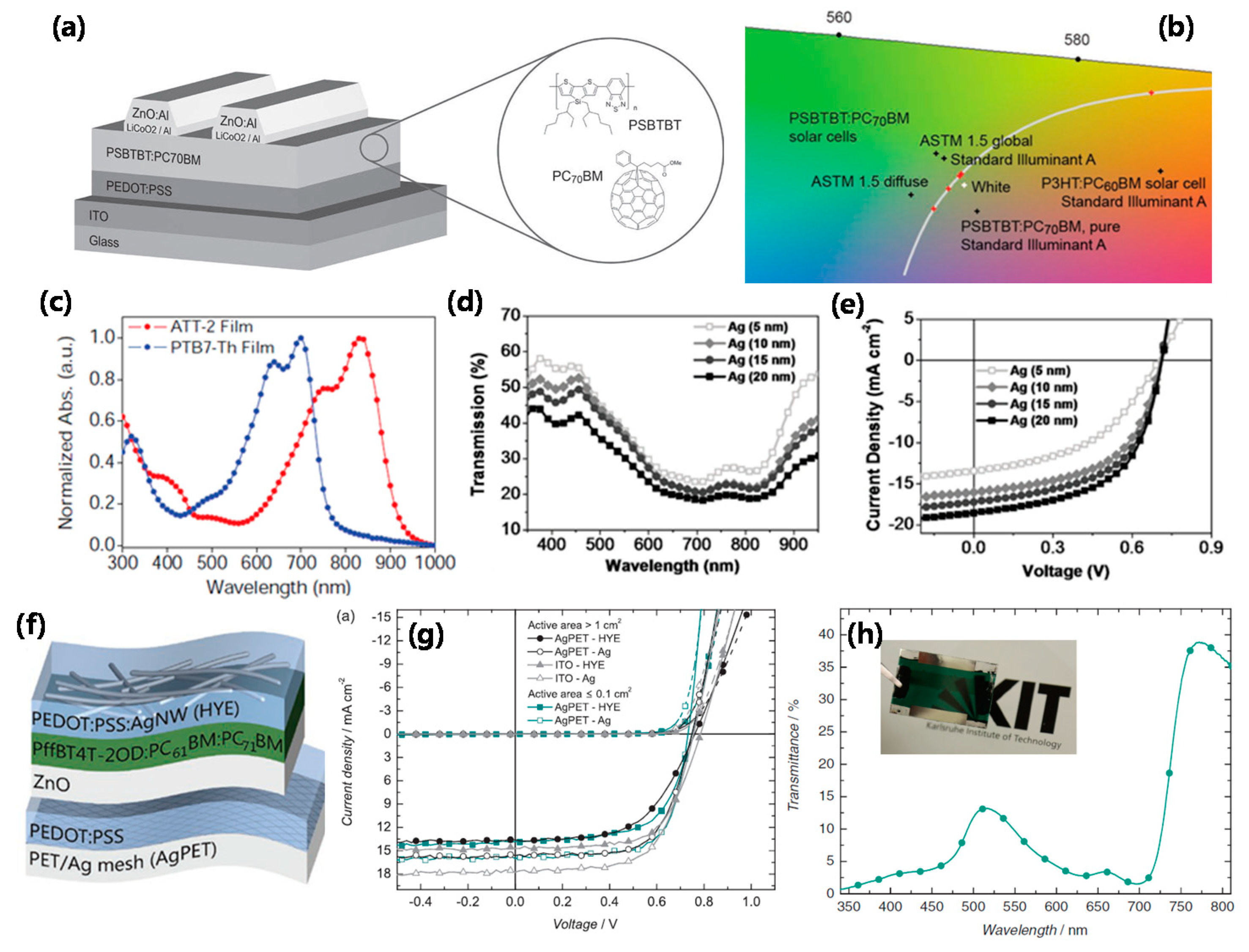
2.3. Corresponding Color Temperature

The human eye can adjust white light perception to any virtual blackbody radiator. The absolute temperature of the black body (full radiator) having the chromaticity closest to that of the white light source color is defined as the correlated color temperature. Chromaticity point cloud group with the same color temperature exists on the black body locus. That is, even though the correlated color temperature is the same, the chromaticity is not the same. In this case, the degree and direction deviating from the blackbody locus are displayed together with the color temperature. The color temperature of the light source at the closest point on the Planckian orbit is referred to as the corresponding color temperature when the color coordinates are in CIE 1931 color space chromaticity.

2.4. Color Rendering Index

As another important parameter, the color rendering properties of STSCs cannot be simply determined from their transparency perception. Therefore, color rendering index (CRI) should be evaluated for presenting the degree of the variation between the transmitted and the incident lights for the cells. The CRI of a STSC is evaluated from the transmitted light, following the standard CIE procedure, and is scaled from 0 to 100. Higher CRI indicates better color rendering capacity, i.e., higher neutral color degree. In other words, the higher the CRI, the more the transmitted light that can adequately represent the color, and the lower the CRI, the less the ability to express color. The CRI of STSCs is influenced by a number of factors such as device architecture, active material, and electrode transmittance. Several methods have been employed to improve the CRI of STSCs. For example, the use of the materials with low band gap [45,46] or complementary optical absorption [63] and the combination of dyes for the active layer [90] have been proposed, but most CRI values must be compromised with the device compliance. Recently, a new strategy has been developed to improve the CRI of STSCs while maintaining the device performance. In this approach, a reflective layer was located on top of the semitransparent metal anode of OSCs, resulting in a CRI close to 100% [91].

3. Semitransparent Organic Solar Cells

Unlike inorganic solar cells, the OSCs have inherent advantages that can provide a wide range of functional abilities for semi-transparent PVMs. Especially, the color of STOSCs can be changed controlled by varying the components of the photoactive layer, useful for aesthetic architectural applications in electric windows of buildings and automobiles [16,92,93]. The transmittance of STOSCs is typically characterized by an AVT measured in the visible range of 370 to 740 nm. For semitransparent solar cells, the front and back electrodes must be transparent, and it is therefore important to develop high-transparency/low-sheet-resistance transparent conductive electrodes (TCEs) that can be easily prepared on the photoactive layer. The material/device design is also essential for achieving high-performance STSCs. For example, theoretical expectations for selecting the photoactive layer and determining the thickness of the electrode are required to obtain optimized current density (Jsc) [94]. Simulating the optical field distribution of the cell while varying the thickness of photoactive layer can help optimize the electrical and optical performance of the cell [95].
The TCEs of STOSCs serve to transmit the light, to transfer the carriers to the photoactive layer, or to provide a distributed electric field by which the carriers transport [96]. Recently, many studies have focused on the development of transparent conductive oxide (TCO)-free TCEs such as conductive polymers, carbon nanotubes (CNTs), graphene, ultra-thin metal films, and metal nanowires (NWs). The TCO-free TCE-based STOSCs are discussed in the following sections.

3.1. Transparent Conductive Electrodes for Semitransparent Organic Solar Cells

3.1.1. Transparent Conducting Polymers

Transparent conductive polymers are regarded as attractive electrodes for STOSCs because they can be prepared on a large area in an easy and simple way. In particular, poly(3,4-ethylenedioxythiophene):poly(styrenesulfonate) (PEDOT:PSS) among various transparent conductive polymer electrode materials have been intensively employed for STOSCs [97,98]. Recently, a structure of PEDOT:PSS CPP 105D (H.C.Starck GmbH, Goslar, Germany) (CPP-PEDOT:PSS)/poly(3-hexylthiophene) (P3HT):phenyl-C61-butyric acid methyl ester (PC61BM)/ZnO/indium tin oxide (ITO) for STOSCs has been studied by using ITO and PEDOT:PSS as the bottom cathode and the top anode, respectively, thereby showing a PCE of 2.4% [27]. In another approach, an ITO/polyethylene oxide (PEO)/poly[2,7-(9,9-dioctylfluorene)-alt-5,5-(4,7′-di-2-thienyl-2′,1′,-3-benzothiadiazole) (APFO3):PC61BM/low-conductive PEDOT:PSS P VP Al 4083 (PEDOT-EL)/PH500 PEDOT:PSS-type OSC employing PEO as a reflector has exhibited a PCE of 0.7% [28]. In the same structure, by inserting poly(allylamine hydrochloride)-dextran between the PEDOT:PSS electrode and the active layer and changing the active layer with P3HT:PC61BM, the PCE increased to 1.86% [29]. When P3HT:IDT-2BR (non-fullerene acceptor) as a photoactive layer and PH1000 PEDOT:PSS as a top electrode were used for semitransparent, non-phenylene, and flexible OSCs, resulting PCE and AVT were 2.88% and ~50%, respectively, as shown in Figure 1 [30]. These results show the possibility of further progress in the performance of the STOSCs with transparent conducting polymer electrodes in near future, but the improvement may be limited due to the inherently-low conductivity (high sheet resistance) of the transparent conducting polymers.

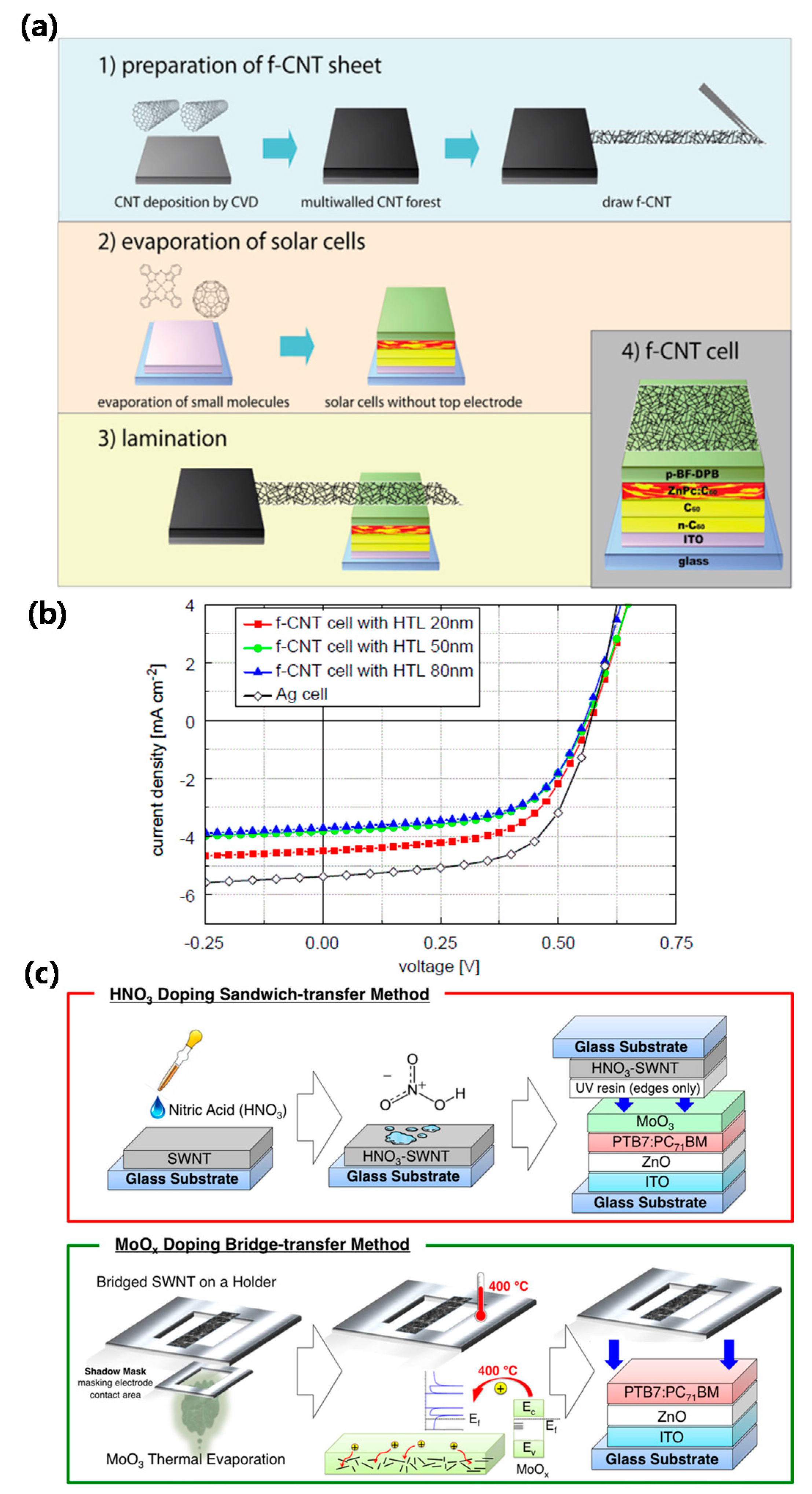
3.1.2. Carbon Nanotubes
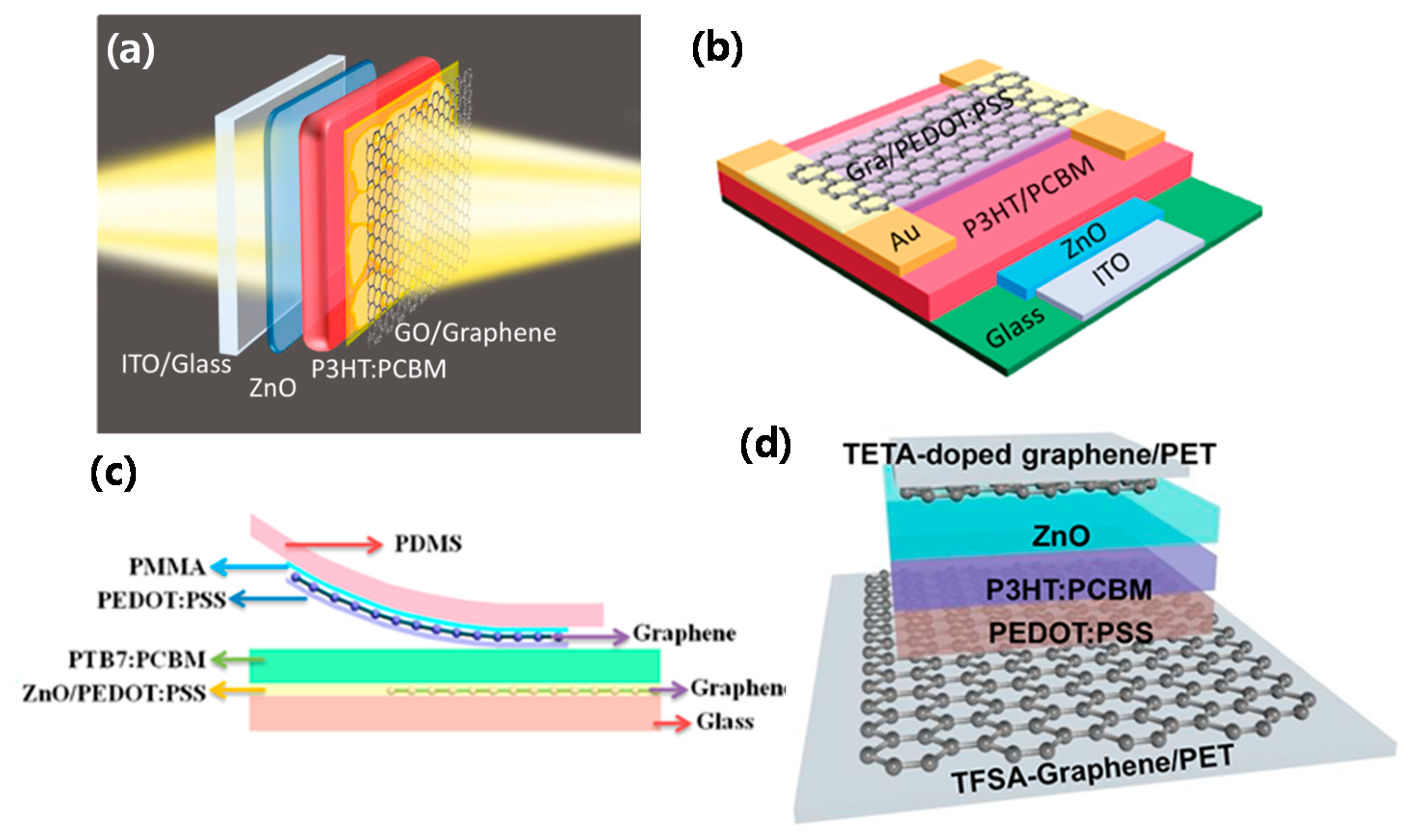
CNTs are attractive for flexible electrodes due to the uniform transparency in the entire visible wavelength range, intrinsically excellent electrical characteristics, high flexibility, and simple solution process at room temperature [99,100]. The resistance of a CNT network is determined by the contact resistance between the CNTs and their individual resistance, depending on length, diameter, metallic/semiconducting volume ratio, synthesis method, and purity. In addition, the surface roughness of CNT films is another major factor as a TCE for OSCs because it can result in significant shunt resistance loss. Recently, free-standing multi-walled-CNTs (f-MWCNT)-based STOSCs have been fabricated by depositing f-MWCNTs on the active layer by room-temperature self-laminating process [31], as shown in Figure 2a. Figure 2b shows current density-voltage (J-V) curves of the zinc phthalocyanine (ZnPc):C60-based STOSCs as a function of hole transfer layer (HTL) thickness, resulting in 60% FF and 1.5% PCE at a HTL thickness of 20 nm. In another approach, STOSCs with CNT film TCE and P3HT:PC61BM as the active layer showed 2.48% PCE and 60%–80% transmittance in the NIR region [32]. As a different structure, MoO3/PTB7: [6,6]-Phenyl-C71-butyric Acid Methyl Ester (PC71BM)/ZnO/ITO-type STOSCs employing single-wall CNTs exhibited 1.8% PCE and ~80% transmittance in the visible light range of 400 to 800 nm [33]. Figure 2c shows fabrication processes of STOSCs using CNTs p-type-doped by two steps: HNO3 doping through ‘sandwich transfer’ and MoOx thermal doping through “bridge transfer”. Resulting PCE of the STOSC using the thin-CNT with 90% transmittance in the visible light region was 3.7%, but the PCE was about 50% lower compared to non-transparent metal-based solar cells (7.8%).

3.1.3. Graphene

Graphene is very useful as a TCE for OSCs thanks to its inherently-high chemical/thermal stabilities, excellent mechanical properties, and small contact resistance with organic materials. Graphene can be fabricated by several techniques such as mechanical exfoliation, laser-induced exfoliation, reduction of graphite oxide (rGO), unzipping of carbon nanotubes, chemical synthesis, and chemical vapor deposition (CVD) [101]. Among these, rGO and CVD are most promising in view of mass-production of flexible TCEs.
Recently, STOSCs using a top-laminated graphene electrode have been successfully fabricated without any damage in the underlying organic photoactive layer, as shown in Figure 3a [34]. The PCE of the STOSCs reached approximately 76% of what was obtained from the counterpart cells using opaque-type Ag metal electrodes. These results are promising in that low-cost STSCs can be fabricated by using graphene TCEs, and are possibly useful for power-generated windows and multi-junction or bifacial photovoltaic panels. As another approach, STOSCs with P3HT and PC61BM were fabricated by employing single-layer graphene and ITO as the top and bottom electrodes, respectively (Figure 3b) [35]. Here, the graphene electrodes were hybridized with Au NPs and PEDOT:PSS to enhance their conductance, resulting in a maximum PCE of 2.7% at a 20 mm2 area.
Figure 3c shows a different type of STOSC structure: graphene/PEDOT:PSS/PTB7:PC71BM/ZnO NP/PEDOT:PSS/graphene [36]. The AVT and maximum PCE of the STOSC are ~40% and 3.4%, respectively on both sides. The fabrication method for this cell is compatible with those of other photonic devices because almost all the procedures including transfer of film, spin coating, and lamination were done at low temperatures. Another OSC with a structure of ITO/TiO2/P3HT:PC61BM/PEDOT:PSS/graphene/Au grid/polyethylene terephthalate (PET) exhibited high light transmittance and small sheet resistance, resulting in 2.8% PCE on the graphene side [37].
Very recently, the use of p and n-type graphene TCEs for both electrodes of the STOSC improved conductivity while maintaining good transparency [63]. Figure 3d shows another STOSC consisting of triethylene tetramine (TETA)-doped graphene/ZnO/P3HT:PC61BM/PEDOT:PSS/bis-(trifluoromethanesulfonyl)-amide (TFSA)-doped graphene prepared following a simple solution process. The PCEs of 3.30% and 3.12% were obtained by the irradiation through TFSA-doped and TETA-doped graphene surfaces, respectively, and the transmittance was 30%–40% at ~400 to 550 nm and 70% at ~650 nm. On the other hand, a flexible OSC on PET retained more than 99% of its initial PCE even after inner/outer bending at a curvature radius (R) of 6 mm [38].

3.1.4. Metal Nanowires

Metallic NWs were widely studied for the application as TCEs on flexible substrates due to their high transmittance, small sheet resistance, and excellent mechanical flexibility, especially useful for reducing the overall cost of the mass production [102]. For example, the Ag NWs electrode is a good alternative to ITO because the energy payback time of the modules is reduced almost 17% by use of the former [103]. Recently, metal NWs as a TCE have received much attention due to their outstanding electrical and optical properties. Especially, Ag NWs are very useful as solution-processable TCE for the application in the STOSCs [104,105,106,107,108,109] STOSCs were also fabricated using laminated Ag NWs meshes without damaging the photoactive layer in 2010 [39], thereby showing an AVT of 26% in the spectral range of 400 to 800 nm and a low PCE of 0.63%.
Recently, there has been a report on P3HT:PC61BM-based STOSCs with Ag NWs as a top electrode [40], whose performance (PCE: 2.1%) was comparable to that of an OSC with thermally-evaporated Ag electrode (PCE: 2.6%). More interestingly, the STOSCs exhibited nearly same optical and device-performance characteristics under illumination on both sides. The OSCs with Ag NWs as both electrodes, completely processed by solution treatment [41], showed 2.2% PCE and 30% transmission at a 550 nm wavelength. In particular, they exhibited almost same transmittance in the ultraviolet (UV)-vis-NIR range, not available when ITO was used as one of the electrodes, demonstrating better optical characteristics of Ag NWs. These results indicate important technological progress for fully printed OSCs and further suggest that ITO-free STOSCs can be successfully fabricated.
In another approach, Ag NWs and PH1000 PEDOT:PSS film were employed as both electrodes for translucent and ITO-free OSCs fully solution-processed on P3HT:PC61BM [42]. Figure 4a shows the real image of the OSC fabricated at low temperature, whose transmittance is approximately 55% at wavelengths longer than 650 nm without absorption of the P3HT:PC61BM active layer, as shown in Figure 4b, resulting in 2.3% and 2.0% PCEs under the illumination at the cathode and anode sides, respectively (Figure 4c). This performance is comparable to that of STOSCs with ITO bottom electrodes [34]. To exclude possible damage of the underlying organic photoactive layer by the TCE, the OSCs were produced by using spray-coated Ag NWs-based composites [43]. Here, the used photoactive material was sensitive to the light in the NIR range, but highly transparent to visible light. Figure 4d shows a schematic and a photo image of the cell with a PCE of 4% and a maximum transparency of 66% at 550 nm, as shown in Figure 4e,f. Inkjet printing technique was employed to fabricate Ag NWs electrodes from Ag NWs solutions [44]. The printed Ag NWs mesh showed similar uniformity, conductivity, and transmittance with Ag NW films prepared by conventional methods such as slot die or spray coating. In this study, STOSCs using bulk heterojunction (donor (PV2000): acceptor (PC71BM)) as the active layer and ink-jet-printed Ag NWs mesh as both electrodes showed 4.3% PCE at a 1 cm2 area and about 10% transmittance in the visible range.
As mentioned above, TCEs play an important role in determining the photovoltaic performance of STOSCs. The TCEs such as conducting polymers, CNTs, graphene, and Ag NWs have greatly improved the performance of the STOSCs, but there still remain many issues for further optimization because all the TCEs have trade-off correlations between their sheet resistance and transmittance. For example, STOSCs with high-transmittance/low-conductivity TCEs exhibit excellent transmittance but poor device performance whist those with low-transmittance/high-conductivity TCEs are operated to the contrary. Especially, the conductivity of conducting polymers, CNTs, and graphene are still low despite their excellent transmittance, and therefore limits the performance of STOSCs. If the TCEs with sheet resistances similar or even better than those of TCOs while maintaining high transmittance are successfully developed, solar cells with excellent performance/transparency at the same time can be realized.

3.2. High Color Neutral Perception

In addition to transparency and efficiency as important factors for STOSCs, color perception should be also considered. Color perception is generally determined by photoactive layer materials and electrodes. The transparency color perceptions of STOSCs are described based on the CIE 1931 chromaticity diagram. The coordinates of the white light are (0.33, 0.33), and the closer to (0.33, 0.33) the color coordinates of the STOSCs, the better their color neutrality [16]. The maximum photopic (vision in bright light) and scotopic (vision in dim light) sensitivities of human eye are at 555 and 507 nm respectively. Therefore, the key idea of designing STOSCs is to completely utilize the solar illumination in NIR region by transmitting the light in the range of 400 to 600 nm, most sensitive to human vision [110].

3.2.1. Photoactive Layer Materials

It is important to select photoactive layer materials with strong absorbance in the UV and NIR range to obtain high Jsc and PCE from STOSCs with reasonable visible transparency. Recently, efficient STOSCs were successfully fabricated using a blend of poly[(4,4’-bis(2-ethylhexyl)dithieno[3,2-b:2’,3’-d]silole)-2,6-diyl-alt-(2,1,3-benzothiadiazole)-4,7diyl] (PSBT BT) polymer donor and PC71BM acceptor with long-term absorption power in the IR region, as shown in Figure 5a [45]. The transparent color recognition of the STOSCs was very close to white light (Figure 5b), as confirmed by the color coordinates obtained from the transmission spectrum. Moreover, the STOSCs exhibited remarkable rendering characteristics together with overall PCE of 3%. Another kind of STOSC was fabricated using a photoactive layer composed of low-bandgap polymers [46], thereby showing grayish or neutral color appearance due to the complementary and balanced absorption of the active layers [poly[2,6-(4,4-bis-(2-ethylhexyl)-4H-cyclopenta[2,1-b;3,4-b0] dithiophene)-alt-4,7-(2,1,3-benzothiadiazole)] (PBDTT-C-T) and PC71BM]. As the reflective Ag electrode thickened from 6 to 60 nm, the average visible light transmittance and PCE varied from 36% to 2% and 4.25% to 7.56%, respectively. Furthermore, the CRI of the STOSCs was shown to be close to 100, promising for their power-generating window applications.
As a different method, STOSCs were fabricated by employing a photoactive layer of poly(indacenodithiophene-co-phenanthro[9,10-b]quinoxaline) (PIDT-PhanQ):PC71BM [16]. The STOSCs with a 30 nm Ag cathode exhibited 5.1% PCE, about 25% AVT, and good color recognition close to white light. Other groups used blade coating technology to fabricate a series of STOSCs using different polymer donors [47]. The STOSCs with 6-bis(trimethyltin)-4,8-bis(5-(2-ethylhexyl) thiophen-2-yl)benzo[1,2-b:4,5-b′]dithiophene (PBDTTT-CT):PC71BM and poly[4,8-bis(5-(2-ethylhexyl)thiophen-2-yl)benzo[1,2-b;4,5-b0]dithiophene-2,6-diylalt-(4-(2-ethylhexyl)-3 fluorothieno [3,4-b]thiophene-)-2-carboxylate-2-6-diyl)] (PBDTTT-EFT):PC71BM showed transparent color recognition close to white based on standard light source D65 with CRI of 95.4 and 87.1, respectively. The STOSCs using PBDTTT-CT:PC71BM and PBDTTT-EFT:PC71BM showed 5.2%/3.8% and 5.6%/5.3% PCEs at active area of 0.04/10.8 cm2, respectively. More recently, a small-bandgap electron acceptor (ATT-2) was blended with a polymer donor poly[[2,6′-4,8-di(5-ethylhexylthienyl)benzo[1,2-b;3,3-b]dithiophene][3-fluoro-2[(2-ethylhexyl)carbonyl]thieno[3,4-b]thiophenediyl]] (PTB7-Th) to fabricate nonfullerene STOSCs [48]. Figure 5c shows complementary absorption spectrum of the photoactive blend film, useful for improving the light harvesting, resulting in the increase of Jsc. The STOSCs exhibited excellent color rendering with color coordinates of (0.2805, 0.3076), correlated color temperature of 9113 K, and excellent CRI of 94.1. In addition, the AVT and PCE increased to 37% and 7.74%, respectively due to absorption of light up to the NIR region, as shown in Figure 5d,e.
As a simple approach, ITO-free OSCs were fabricated by employing hybrid top and bottom electrodes and ternary polymer:fullerene photo-active layers [49]. Here, the polymer:fullerene absorber blend poly[(5,6-difluoro-2,1,3-benzothiadiazol-4,7-diyl)-alt-(3,3‴-di(2-octyldodecyl)-2,2′;5′,2″;5″,2‴-quaterthiophen-5,5‴-diyl)] (PffBT4T-2OD):PC61BM:PC71BM and all other functional layers, which are high-efficiency tertiary polymers as active layers, were prepared using a doctor blade method from non-halogenated solvents to meet industrial device manufacturing requirements. Figure 5f shows a schematic diagram of the completed STOSC with maximum PCEs of 6.6% and 5.9% on active areas ≤0.1 cm2 and >1 cm2, respectively (Figure 5g) and 13% peak transparency at 515 nm (Figure 5h). Unlike conventional methods, flexible transparent OSCs using graphene TCEs as both anode and cathode were recently prepared based on a device structure of graphene/PEDOT:PSS/ZnO/poly[2,7-(5,5-bis-(3,7-dimethyl octyl)-5Hdithieno[3,2-b:20,30-d]pyran)-alt-4,7-(5,6-difluoro-2,1,3-benzothiadiazole)] (PDTP-DFBT):PC61BM/MoO3/graphene, thereby showing 3.7% PCE and 54% AVT in the visible regime (400–650 nm) [50]. The PCE was almost invariant after 100 cycles at R = 1.2 mm. As another approach, a highly efficient STOSC device was fabricated based on a novel polymer:non-fullerene (PBDB-T:ITIC) system [51], thereby showing optimized PCE > 7% with an AVT of 25%. These results suggest that optimizing the thickness of the active layer does not only allow images to be displayed accurately but also makes the STOSCs exhibit high efficiency/visible light transmittance. On the other hand, a combination of a cathode modified with transparent ZnMgO and a thin MoO3/Ag anode yielded stable and efficient STOSCs with clear color recognition [52]. In this device, the PCE/AVT, controlled by the thickness of the Ag electrode, was 6.83%/21.6% and 8.58%/0.6% at Ag thicknesses of 10 and 50 nm, respectively. In addition, this method resulted in long-term device life due to the barrier effect on oxygen and water. More importantly, the STOSCs showed a very-long life span, i.e., high PCE of 7.02% even after two-year storage. These results may provide a useful way for developing STOSCs with high efficiency, long lifetime, and excellent color recognition for practical applications. Recently, another group designed and synthesized “IEICO-4Cl”, a nonlelerene receptor with ultra-low band gap, and produced blend films with other polymer donors (poly[4-(4,8-bis(5-(2-ethylhexyl)thiophen-2-yl) benzo[1,2-b:4,5-b′]dithiophen-2-yl)-5,6-difluoro-2-(2-2hexyldecyl)-7-(thiophen-2-yl)-2H-benzo[d][1,2,3]triazole] (J52), poly[(2,6-(4,8-bis(5-(2-ethylhexyl)thiophen-2-yl) benzo [1,2-b:4,5-b′] dithiophene)-co-(1,3-di(5-thiophene-2-yl)-5,7-bis(2-ethylhexyl)benzo[1,2-c:4,5-c′]dithiophene-4,8-dione)] (PBDB-T), and PTB7-Th) [53]. The colors of the blend films such as J52:IEICO-4Cl, PBDB-T:IEICO-4Cl, and PTB7-Th:IEICO-4Cl could be adjusted from purple to blue and cyan, resulting in 10.1%/35.1%, 9.7%/35.7%, and 10.3%/33.5% PCE/AVT, respectively. These results suggest that design and use of ultralow-bandgap nonfullerene acceptor can be an efficient route for enhancing the photovoltaic parameters of STOSCs.

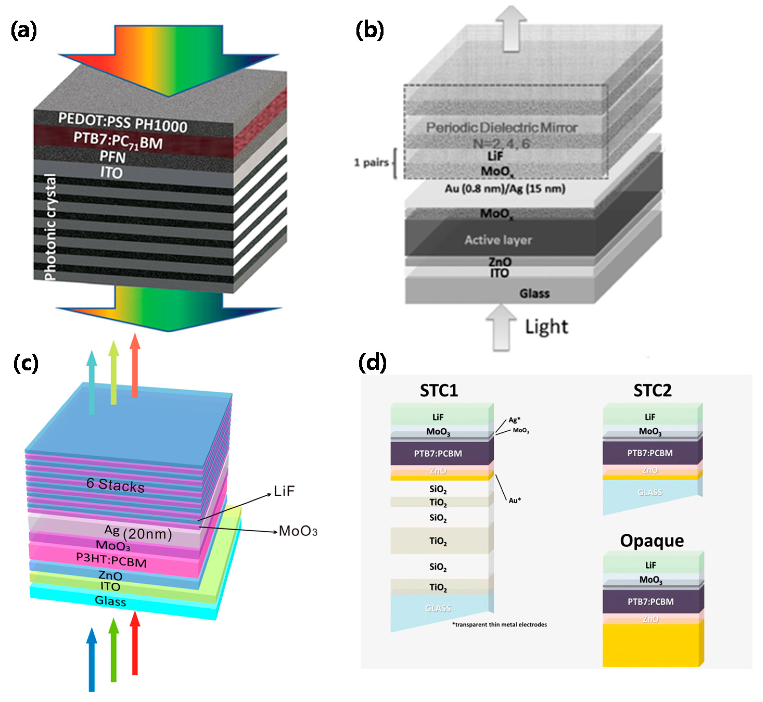
3.2.2. Photonic Crystals
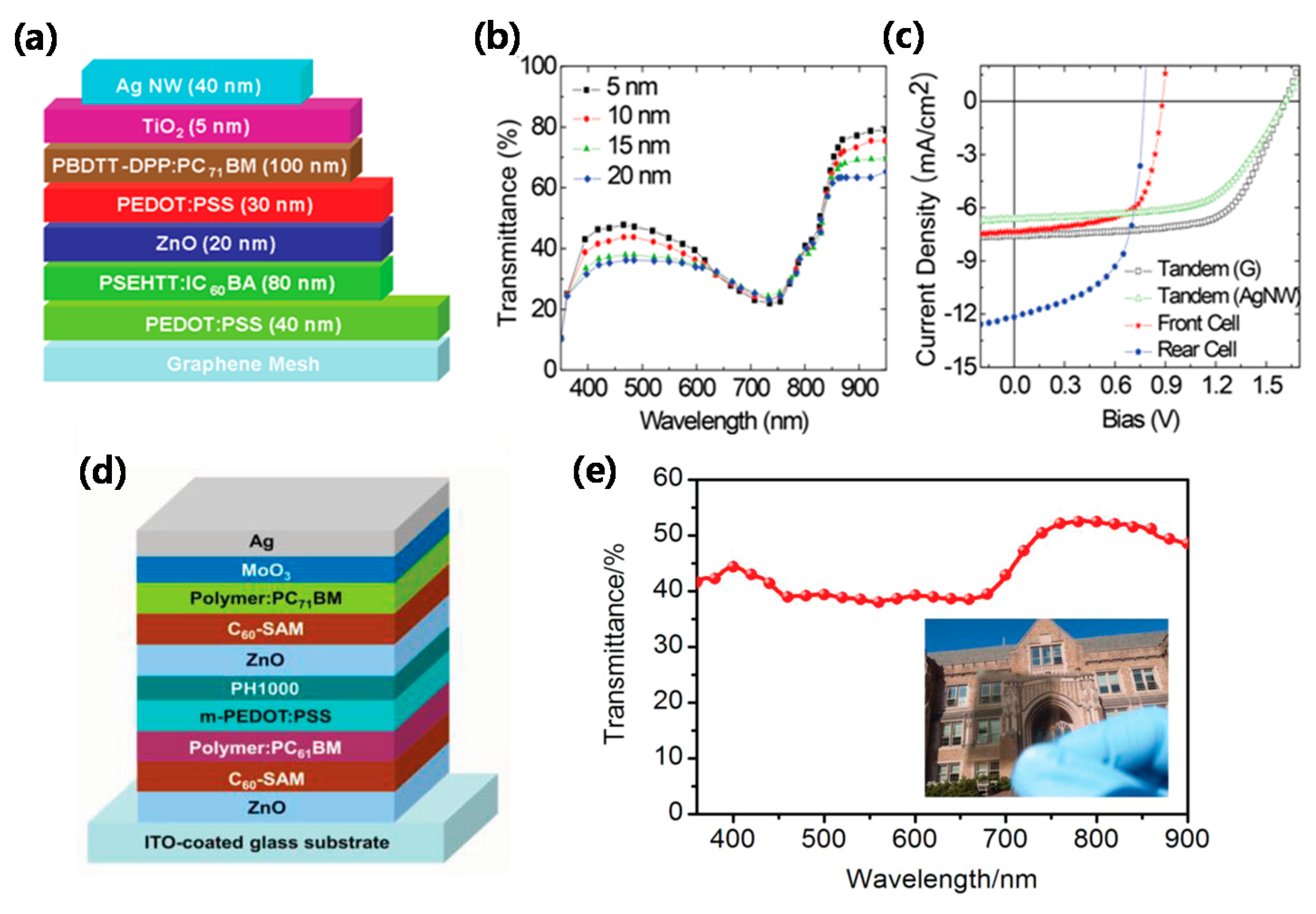
The TCE absorbing only a fraction of the incident light and thinner photoactive layer should be used to maintain overall transmittance of STOSCs. The trade-off between the transmission and the absorption is the main factor for determining the PCE of STOSCs, in contrast with their opaque counterparts. A light-trapping approach should be therefore employed to improve the PCE of STOSCs. Chalesteric liquid crystals were developed in 2011 as an organic wavelength-dependent reflector, which can be fabricated by solution treatment for STOSCs [111]. The cholesteric liquid crystal can be properly adjusted to reflect the light only in the spectral range compatible with that absorbed by the photoactive layer and transmit the light in the other wavelength range. Then, the unabsorbed light that can produce photocurrent (PC) are reflected and reabsorbed by the photoactive layer, resulting in the increase of PC and PCE without reducing the transparency. The PCE was 6% increased when the spectral range of the light reflected by the cholesteric liquid crystal was matched to that absorbed by the cell.
Photonic crystals are nanostructured materials with the dielectric function periodically modulated, which can be employed as a distributed Bragg reflector in OSCs for enhancing the light capture [112,113,114,115]. To trap NIR and near-UV photons for the OSC, another group introduced a new approach for employing aperiodic photonic crystals in 2013 [88]. The photon manipulation by the nonperiodic 1D structure was very effective for enhancing the light harvesting of the STOSCs to 77% of what was achieved from the opaque counterpart cells. By the light trapping technique, the STOSCs exhibited 5.6% PCE and ~30% luminosity. In other study, one-dimensional photonic crystal (1DPC) was prepared on top of the Ag anode for STOSCs as a distribution reflector [54]. By this approach, the PCE has improved by 28% (absolutely from 1.92% to 2.46%) due to high reflectivity close to 100% at 580–780 nm. The AVT of 40% was maintained over the remaining visible wavelength range of 380–580 nm, and this was 33% improvement compared to the cells without 1DPCs. Subsequently, a series of translucent OSCs were fabricated to show further-enhanced PCE and transmittance using 1DPCs as reflectors [55,56,95,116,117,118]. In other report, the fullerene blends were successfully sandwiched between a bottom 1DPC and a top solution-processed highly-conductive PEDOT:PSS, as shown in Figure 6a [55]. Resulting PCE and Jsc were 5.20% and 12.25 mA·cm−2, respectively, 37% and 38% rises compared to the OSCs without 1DPC and highest ever known for inverted OSCs with highly-conductive PEDOT:DOT layer at the illumination side.
Recently, high-quality hybrid Au/Ag transparent top electrodes and 6 pairs of fine-tuned dielectric mirrors (DMs) were employed for inverted OSCs with PTB7-Th:PC71BM, as shown in Figure 6b [56], showing a maximum PCE of 7.0% with an AVT of 12.2%. This PCE was highest ever reported for translucent PSCs as well as 81.4% of what was obtained from the opaque counterparts. Similar device design and processing methods were also successfully applied to flexible substrates, thereby achieving 6.4% PCE and 11.5% AVT. As a different method, 6 pairs of MoO3/LiF layers (60 nm for MoO3 and 90 nm for LiF, respectively) were used as reflectors to fabricate STOSCs, as shown in Figure 6c [57]. By the optimization of the reflector structure, enhanced light harvesting was obtained, resulting in an increase of Jsc from 8.1 to 10.9 mA·cm−2 (the increase of the PCE from 3.36% to 4.32%), caused by the enhanced reflection of the light in the wavelength range of 450 to 600 nm, corresponding to the wavelength range of the absorption by the active layer.
According to another approach, PTB7:PC71BM blend active material were employed to enhance the light trapping inside the STOSC [58]. The multilayer dielectric structure (MLD) of the STOSCs was made to improve external quantum efficiency in the UV and NIR wavelength range with the transparency in the visible region being almost unchanged [54]. In this study, two types of STOSCs (STOSC1 and STOSC2) and opaque cells (reference) were fabricated to better evaluate the photovoltaic performance of STOSCs (Figure 6d). The Jsc of the STOSC1 containing this cavity configuration was 10.7 mA·cm−2, 96.4% of what was obtained from the opaque counterpart cell, resulting in a PCE of 5.3%, comparable to that (5.9%) of the opaque cell. On the other hand, the Jsc of the STOSC2 was lower due to the lack of effective optical trapping effect.

3.2.3. Tandem Cells

Tandem OSCs have the advantage of maximizing the absorption of the solar energy by stacking two or more different cells that respond to different parts of the solar spectrum. The absorption, transparency, and efficiency of the cell can be also finely adjusted by constructing a series of stacks by introducing multiple of photoactive materials [59]. Two semitransparent sub-cell stacks were connected in parallel to enhance the PCE of OSCs in 2012 [60]. The total loss of light in the semitransparent tandem solar cells by the reflection, parasitic absorption, and transmission can be less than that in a single cell with the same photoactive materials. In this study, a new and efficient STOSC was constructed using polymer poly(3,3′-([(9′,9′-dioctyl-9H,9′H-[2,2′-bifluorene]-9,9-diyl)bis(4,1-phenylene)]bis(oxy))bis(N,N-dimethylpropan-1-amine)) (PFPA-1) modified ITO bottom cathode and high conductivity PEDOT: PSS PH1000 top anode, thereby showing PCE of 3.35% and 2.61% depending on the composition of the active layer with poly[N,N′-bis(2-hexyldecyl)isoindigo-6,6′-diyl-alt-thiophene-2,5-diyl] (P3TI):PC71BM and poly[2,3-bis-(3-octyloxyphenyl)quinoxaline-5,8-diyl-alt-thiophene-2,5-diyl] (TQ1):PC71BM, respectively. Furthermore, a series of tandem solar cells using two cells were also fabricated to exhibit an efficiency of 4.35%. In a different approach, semitransparent tandem OSCs were fabricated using graphene meshes and laminated Ag NWs, each of which was solution-treated for a transparent anode and a cathode, respectively (Figure 7a) [61]. In this study, the AVT was adjusted from 44.9% to 39.9% as the thickness of TiO2 increased from 5 to 20 nm, as shown in Figure 7b. In the same range of TiO2 thickness, the Jsc decreased from 7.62 to 5.90 mA·cm−2, resulting in the decrease of the PCE from 8.02% to 5.52%.
As a final issue, when the light was incident at the side of the graphene-mesh electrode, the PCE was remarkably enhanced to 8.02% with an average transmittance of 44.9%, but the irradiation from the stacked Ag NW side resulted in a PCE of 6.47% (Figure 7c). Alternatively, for the production of high-efficiency tandem STOSC, the same polymer donor blended with PC61BM and PC71BM were used as the active layer, as shown in Figure 7d [62]. The tandem cells using PIDT-phanQ and same middle-bandgap polymer showed a high open circuit voltage (Voc) of 1.71 V, thereby achieving a high PCE of 8.5%. Since the total active layer is very thin, the PIDT-phanQ can be used as a donor for very efficient semitransparent tandem cells. As shown in Figure 7e, around 40% AVT was obtained, promising for their use in power window applications. In addition, tandem architecture OSCs were configured to adjust the external appearance from visible transparency to semitransparency [63], resulting in 7.3% PCE and 30% AVT. Interestingly, the photovoltaic properties of these tandem OSCs did not differ significantly from those at the top and bottom lighting modes. As shown above, the trade-off relation between the transmittance and absorption of the photoactive layers affects the performance and transparency of STOSCs, and the related parameters should be therefore systematically adjusted through the improvement of the photoactive layer and the manipulation of the cell architecture.

4. Semitransparent Perovskite Solar Cells

PSCs have received much attention in recent years due to their high efficiency and low-cost solution processibility [119,120,121]. The photoactive layer of PSCs, organic-inorganic metal halide perovskites, can be prepared on flexible substrates by low-temperature solution treatment, similar to OSCs. The bandgap and thickness of perovskite films can easily be adjusted to be semitransparent in the visible region, especially useful for flexible and translucent PSCs. Considering the close correlation and strong similarities between planar PSCs and OSCs, this section will review the progress of the semitransparent planar PSCs to provide the reader with an overall understanding for the state of the art of this research field. The STPSCs are also highly attractive due to their potential applications in building integrated photovoltaics and smart glasses. The principal difference between STPSCs and STOSCs is the optically active layer. In general, the transparency of the perovskite film in STPSCs is smaller than that of the organic photoactive layer in STOSCs because the perovskite film is thicker and more absorptive. The transparency of the perovskite film can be enhanced by decreasing the surface coverage of the island structure or by simply reducing its thickness. In addition, the performance of STPSCs depends on the electrode type of the cell, similar to STOSCs.

4.1. Single-Junction Cells

4.1.1. General Trend

Typically, the device architecture of PSCs is classified as n-i-p (normal) and p-i-n (inverted) types in terms of what type of material is placed on the TCO such as FTO or ITO. A metal electrode with proper work function was used as the top electrode. Recently, microstructure array of the “island” perovskite for STPSCs were formed by dewetting process, as shown in Figure 8a [64]. Figure 8b shows a scanning electron micrograph (SEM) of top surface of a typical film composed of perovskite islands (paler regions) on a TiO2-coated FTO substrate. Figure 8c shows a photo image of a STPSC formed on glass. The correlation between the transmittance and the PCE of the cell was controlled by the surface coverage of the perovskite active layer. The average PCE is 7% when the perovskite surface coverage is 100%, but the AVT is 7% due to the low transmittance, as shown in Figure 8d. However, the cells with highest AVT of about 30% showed about 3.5% PCE. As another approach, a macroporous perovskite semitransparent film was aligned with FTO glass by a sacrificial polystyrene (PS) microsphere template [65] because the macropores inside the perovskite film was known to increase the light transmittance. Thus, the AVT in macroporous perovskite films was adjusted from 20% to 45% by simply changing the PS diameter and precursor concentration. The STPSCs optimized with the macroporous perovskite film showed 36.5% AVT and 11.7% PCE. All cells showed relatively-low Voc due to the poor shape and crystallinity of the perovskite film.
It was also possible to produce STPSCs with excellent transparency in the visible region by using copper thiocyanate (CuSCN) HTL to reduce the thickness of the perovskite film [66]. Figure 9a,b shows a schematic of a typical CuSCN HTL-based high-efficiency STPSC and its corresponding energy band diagram. Figure 9c shows the transmittance for various thicknesses of perovskite films coated on CuSCN/ITO coated glass, resulting in the variation of the PCE and AVT. The PCE increases from 3.39% to 7.73% as the thickness increases from 40 to 280 nm, but the AVT decreases from 35% to 10% in the same range of thickness (Figure 9d,e). In addition, the use of an extremely thin Au layer as an electrode helped minimize parasitic absorption, and the LiF capping layer played a decisive role in decreasing the energy loss through the specular reflection, resulting in the improvement of the transparency [67]. Consequently, based on a simple cell architecture without need for high temperature processes, the STPSCs showed the AVT close to 29% and highest PCE of 6.4%. In another method using a MoO3/Au/MoO3 top electrode, a STPSC with orange-brown color was successfully fabricated through perovskite thickness control [68]. This cell showed 5.3% PCE/31% AVT at 55 nm and 13.6% PCE/7% AVT at 290 nm. Another group developed STPSCs based on a structure of ITO/PEDOT:PSS/MAPbI3/PC61BM/C60/11-amino-1-undecanethiol hydrochloride/Ag [69]. Here, 110 nm thin perovskite film was used to show high performance of 8.2% PCE and 34% AVT. STPSCs were also fabricated using the island structure-MAPbI3−xClx-NiO composite and the interfacial modification with Al2O3/NiO layer [70]. Resulting performance was 10.06% PCE and 27% AVT together with excellent air stability over 270 days.

4.1.2. Use of TCO Electrodes

As mentioned above, the metal electrodes are limited in their use for improving the transmittance of STSCs. Since TCO has low resistivity and broadband transparency, it is expected that the efficiency and the transmittance of STPSCs can be improved if TCO electrodes are used at the both sides. Recently, STPSCs were fabricated based on a simple structure of FTO/TiO2/MAPbI3/hole transport materials and PEDOT:PSS/ITO [71]. The AVT and PCE of the cells were varied from 17.3% and 12.55% to 6.3% and 15.80% by adjusting the thickness of the MAPbI3 layer. Another group fabricated high-efficiency semitransparent planar PSCs by high-frequency magnetron sputtering at room temperature [72], where hydrogenated indium oxide (In2O3:H) with high mobility was used as the transparent rear electrode, thereby showing 14.2% PCE. These cells also exhibited an additional 13.5% power improvement (absolutely, 20.5% PCE) when operated in a double-sided cell with a perovskite top cell and a copper indium gallium diselenide (CIGS) bottom cell in a 4-terminal tandem configuration. In another approach, a highly efficient translucent sandwich-type MAPbI3 island PSCs were fabricated by employing a PS passivation interlayer to prevent the TiO2 electron conductor and the poly[bis(4-phenyl)(2,4,6-trimethylphenyl)amine (PTAA) hole conductor from being directly contacted [73]. The selective deposition of the PS passivation interlayer on bare TiO2 or between MAPbI3 island crystals was done by a spin-washing process using toluene solvent. Resulting PCE and AVT were 10.2% and 20.9%, respectively. The same group reported semitransparent neutral-color sandwich-type MAPbI3 perovskite submodules (active area = 25 cm2) [74]. In this study, UV-curable monomer compounds coated on island-shaped MAPbI3 were successfully employed to fabricate highly-efficient translucent solar cells by preventing the HTL and the TiO2 blocking layer from being directly contacted. Here, 40 cells were measured to show 10.28% ± 0.96% PCE and 20.1% AVT.

4.1.3. Use of One or Both TCO—Free Electrodes

As described in the previous section, TCO-free TCEs such as PEDOT:PSS, Ag NWs, CNT, and graphene have many advantages for their use in STPSCs. Recently, STPSCs were fabricated based on a structure of Al2O3/Ag NWs/ZnO/MAPbI3/PEDOT:PSS/ITO, as shown in Figure 10a [75]. Here, low temperature treatment (below 100 °C) and atomic layer deposition (ALD) of ZnO and Al2O3 films for the cathode buffer layer (CBL) and encapsulation layers were employed for very efficient and environmentally stable STPSCs. The cells with reflective opaque Ag electrodes showed remarkable PCE of up to 16.5% with high repeatability. In addition, the use of ALD ZnO CBL in STPSCs resulted in 25.5% AVT and 10% PCE. These results can provide a new route for developing highly-efficient, stable, low-temperature-processed semitransparent photovoltaic cells, indicating significant advancements in the practical application of PSCs. In another approach, efficient STPSCs were fabricated using solution-treated Ag NWs top electrodes made with careful selection of reasonable interface engineering and deposition techniques [76]. In this study, the ZnO layer inserted between the ETL PC61BM and the upper electrode Ag NWs did not only allow the Ag NW solution deposition without damaging the PC61BM layer, but also ensured the ohmic contact between PC61BM/ZnO and ZnO/Ag NWs. The resulting translucent PSCs showed high PCE of 8.5% and an AVT of 28.4%. These results suggest that high-performance PSCs can be realized by integrating low-cost materials and following a completely liquid processing path, thereby greatly reducing the production cost. As a different approach, very robust PSCs were prepared by using a translucent top electrode sandwiched between an ultra-thin Ag layer and SnOx grown by low-temperature ALD [77]. Figure 10b shows a SEM of the STPSC produced in this study. Here, SnOx acts as an electrically conductive transmission barrier to protect the perovskite film and ultra-thin Ag electrodes from moisture. The STPSC showed an average transmittance of about 70% for wavelength >800 nm in the NIR region and an efficiency of 11% or more with an average transmittance of 29% at wavelength of 400–900 nm. In addition, the cells exhibited remarkable stability over 4500 h regardless of ambient atmosphere or to elevated temperatures. Another group reported STPSCs using PEDOT:PSS film as a TCE, as shown in Figure 10c [78]. The PEDOT:PSS electrode was deposited using transfer lamination technology to escape from the damage to the MAPbI3 perovskite membrane by direct contact of PEDOT:PSS aqueous solution. The STPSCs showed approximately 10.1% PCE and 7.3% AVT for active area 0.06 cm2. Recently, high-efficiency STPSCs without TCO was manufactured using PEDOT:PSS electrode which can be manufactured under low-temperature and vacuum-free environments [79]. These cells showed high PCEs of 13.9% and 10.3% on glass and PET substrates, respectively. In addition, the flexible substrate-based PSCs retained more than 90% of its initial value even after 1000-cycles bending at a small radius of 5 mm. In more recent years, other groups have successfully produced carbon-grid electrodes that are fully printable on STPSCs [80]. In this study, the AVT/PCE was varied from 6.5%/11.3% to 24.0%/5.1% by controlling the spacing between the carbon grid lines. Finally, by employing MWCNTs to the top electrode of the cell, the PCE was improved to 8.21% while maintaining 24.0% AVT. These results suggest that CNT-based carbon grids provide a low-cost route to fabricate highly-efficient STPSCs. CVD multilayer graphene was also employed for STPSCs (Figure 10d) [81]. By adjusting the preparation conditions, the cells exhibited the average PCE up to 12.02% and 11.65% under irradiation at the bottom and top electrode sides, respectively.

4.2. Multi-Junction Cells

The photoactive layer used in a single-junction solar cell is limited in absorbing all of the sunlight due to its inherent bandgap properties. To solve this problem, multi-junction solar cells have been actively studied by employing two or more optically absorbing semiconductors complementary to each other, stacked vertically to minimize transmitted or heat-lost energy. Multi-junction or tandem solar cells were developed primarily in two schemes, mechanically-stacked 4-terminal and monolithic 2-terminal configurations. In case of perovskites, it is possible to control the bandgap easily by a solution process, thereby making the thin films with high extinction coefficient. High efficiency can be then achieved by reducing losses through the conventional tandemization with a crystalline Si (1.1 eV) or CIGS (1.1 eV) solar cells. Recently, perovskite/c-Si tandem solar cells were successfully produced to show the PCE up to 14.5% [82]. Figure 11a shows a schematic diagram of a typical perovskite/Si tandem solar cell. The PCE of the single-junction cells of perovskite (0.25 cm2) and Si (1.22 cm2) reached 14% and 16.8%, respectively. The PCE of the hybrid tandem solar cell was improved to 19.2% at a 1.22 cm2 area, as shown in Figure 11b. Both PCEs were much better than those of the single-junction counterpart cells. This single-junction and tandem PSCs showed no hysteresis and were very stable under maximum power point tracking for several min (The inset of Figure 11b). Another group studied translucent perovskite solar cells and IR-enhanced Si heterojunction cells for high-efficiency serial devices [83]. The STPSCs were fabricated by thermally depositing a semitransparent metal electrode (7 nm Au/1 nm Cu seed layer) with excellent electrical conductivity and optical transparency. The STPSC and Si cells showed 16.5% and 21.2% PCEs, respectively whilst the perovskite/Si tandem solar cells exhibited 23.0% PCE. In a different study, dielectric/metal/dielectric transparent top electrodes were successfully fabricated for hybrid halide PSC [84]. The Au-coated Ag film significantly enhanced the electrical conductivity and transparency of the electrodes compared to the separate Ag or Au film due to the change of the wetting properties of the metal deposition. The STPSC irradiated from the multilayer top electrode showed 11.5% PCE together without reduction of Voc and FF compared to the conventional cells. Figure 11c shows the 4-terminal serial tandem cell with the PSC top single cell solution-processed on the bottom CIGS single cell. Figure 11d shows the J-V curve of single and tandem cells, resulting in 15.5% PCE for the tandem cell. These results possibly provide a useful route for further enhancement of the PCE by choosing tandem-type perovskite/CIGS solar cell. Another tandem solar cell was also obtained by mechanically placing an Ag NWs-TCE-based PSC on CIGS solar cell and low-quality polycrystalline Si [85], thereby realizing low-cost and high-efficiency (>25%) solar-energy source.

5. Conclusions and Outlook

In the last decade, there have been rapid progress in the studies of STOSCs and STPSCs by developing new flexible bottom/top TCEs, performing the processes at low temperatures, designing/synthesizing high-quality photoactive layers, and engineering device structures. To date, many researchers have made much efforts to achieve high PCE/AVT for the STOSCs and STPSCs, but there still remain several issues to overcome for their practical applications. The PCE and AVT of the semitransparent cells is currently much lower than those of their opaque counterpart cells, and their neutral transparency color perceptions can be hardly achieved. Therefore, the TCEs for STSCs are required to be highly transparent/conductive, a way to minimize the performance degradation while maintaining the device transparency. In addition, the TCEs should be structured for their good tolerance to defects and easy patterning, and should be available for mass production at low cost. To fundamentally improve the PCE/AVT of the STOSCs and STPSCs, new TCEs with the desired optical, electrical, and structural properties are ultimately necessary. Ideally, most of the photons in the UV and NIR range are absorbed by band gap engineering of the material because the composition of organic semiconductors and perovskite materials can be fully controlled. In addition, the color and transparency of the device can be adjusted by introducing periodic 1D dielectric mirrors with enhanced optical reflectivity in selected wavelength range to recapture unabsorbed photons. Although there still remain problems to be solved, STOSCs and STPSCs are expected to contribute greatly to harvesting of solar energy with high efficiency/semitransparency in the near future.

Funding

This research was funded by the Ministry of Science and ICT supported by Basic Science Research Program through the National Research Foundation of Korea (NRF) (NRF-2017R1A2B3006054).

Conflicts of Interest

The authors declare no conflicts interest.

References

  1. Gaur, A.; Tiwari, G.N. Performance of photovoltaic modules of different solar cells. Sol. Energy 2013, 2013, 734581. [Google Scholar] [CrossRef]
  2. Green, M.A.; Hishikawa, Y.; Dunlop, E.D.; Levi, D.H.; Hohl-Ebinger, J.; Ho-Baillie, A.W.Y. Solar cell efficiency tables. Prog. Photovolt. Res. Appl. 2018, 26, 427–436. [Google Scholar] [CrossRef]
  3. Green, M.A.; Ho-Baillie, A.; Snaith, H.J. The emergence of perovskite solar cells. Nat. Photonics 2014, 8, 506–514. [Google Scholar] [CrossRef]
  4. Brittman, S.; Adhyaksa, G.W.P.; Garnett, E.C. The expanding world of hybrid perovskites: Materials properties and emerging applications. MRS Commun. 2015, 5, 7–26. [Google Scholar] [CrossRef] [PubMed]
  5. O’Regan, B.; Grätzel, M. A low-cost, high-efficiency solar cell based on dye-sensitized colloidal TiO2 films. Nature 1991, 353, 737–740. [Google Scholar] [CrossRef]
  6. Martinson, A.B.F.; Elam, J.W.; Liu, J.; Pellin, M.J.; Marks, T.J.; Hupp, J.T. Radial electron collection in dye-sensitized solar cells. Nano Lett. 2008, 8, 2862–2866. [Google Scholar] [CrossRef] [PubMed]
  7. Bagnis, D.; Beverina, L.; Huang, H.; Silvestri, F.; Yao, Y.; Yan, H.; Pagani, G.A.; Marks, T.J.; Facchetti, A. Marked alkyl- vs. alkenyl-substitutent effects on squaraine dye solid-state structure, carrier mobility, and bulk-heterojunction solar cell efficiency. J. Am. Chem. Soc. 2010, 132, 4074–4075. [Google Scholar] [CrossRef] [PubMed]
  8. Zhou, N.; Prabakaran, K.; Lee, B.; Chang, S.H.; Harutyunyan, B.; Guo, P.; Butler, M.R.; Timalsina, A.; Bedzyk, M.J.; Ratner, M.A.; et al. Metal-free tetrathienoacene sensitizers for high-performance dye sensitized solar cells. J. Am. Chem. Soc. 2015, 137, 4414–4423. [Google Scholar] [CrossRef] [PubMed]
  9. Yella, A.; Lee, H.-W.; Tsao, H.N.; Yi, C.; Chandiran, A.K.; Nazeeruddin, M.K.; Diau, E.W.-G.; Yeh, C.-Y.; Zakeeruddin, S.M.; Grätzel, M. Porphyrinsensitized solar cells with cobalt (II/III)-based redox electrolyte exceed 12% efficiency. Science 2011, 334, 629–634. [Google Scholar] [CrossRef] [PubMed]
  10. Mathew, S.; Yella, A.; Gao, P.; Humphry-Baker, R.; Curchod, B.F.E.; Ashari-Astani, N.; Tavernelli, I.; Rothlisberger, U.; Nazeeruddin, M.K.; Grätzel, M. Dye-sensitized solar cells with 13% efficiency achieved through the molecular engineering of porphyrin sensitizers. Nat. Chem. 2014, 6, 242–247. [Google Scholar] [CrossRef] [PubMed] [Green Version]
  11. Kakiage, K.; Aoyama, Y.; Yano, T.; Oya, K.; Fujisawa, J.; Hanaya, M. Highly-efficient dye-sensitized solar cells with collaborative sensitization by silyl-anchor and carboxy-anchor dyes. Chem. Commun. 2015, 51, 15894–15897. [Google Scholar] [CrossRef] [PubMed]
  12. Selvaraj, P.; Baig, H.; Mallick, T.K.; Siviter, J.; Montecucco, A.; Lib, W.; Paul, M.; Sweet, T.; Gaoc, M.; Knox, A.R.; et al. Enhancing the efficiency of transparent dye-sensitized solar cells using concentrated light. Sol. Energy Mater. Sol. Cells 2018, 175, 29–34. [Google Scholar] [CrossRef]
  13. Yoon, S.; Tak, S.; Kim, J.; Jun, Y.; Kang, K.; Park, J. Application of transparent dye-sensitized solar cells to building integrated photovoltaic systems. Build. Environ. 2011, 46, 1899–1904. [Google Scholar] [CrossRef]
  14. Chen, D.; Huang, F.; Cheng, Y.B.; Caruso, R.A. Mesoporous anatase TiO2 beads with high surface areas and controllable pore sizes: A superior candidate for high-performance dye-sensitized solar cells. Adv. Mater. 2009, 21, 2206–2210. [Google Scholar] [CrossRef]
  15. Li, D.; Qin, D.; Deng, M.; Luo, Y.; Meng, Q. Optimization the solid-state electrolytes for dye-sensitized solar cells. Energy Environ. Sci. 2009, 2, 283–291. [Google Scholar] [CrossRef]
  16. Chueh, C.-C.; Chien, S.-C.; Yip, H.-L.; Salinas, J.F.; Li, C.-Z.; Chen, K.-S.; Chen, F.-C.; Chen, W.-C.; Jen, A.K.-Y. Toward high-performance semi-transparent polymer solar cells: Optimization of ultra-thin light absorbing layer and transparent cathode architecture. Adv. Energy Mater. 2013, 3, 417–423. [Google Scholar] [CrossRef]
  17. Ye, L.; Zhang, S.; Zhao, W.; Yao, H.; Hou, J. Highly efficient 2D-conjugated benzodithiophene-based photovoltaic polymer with linear alkylthio side chain. Chem. Mater. 2014, 26, 3603–3605. [Google Scholar] [CrossRef]
  18. Park, N.-G. Perovskite solar cells: An emerging photovoltaic technology. Mater. Today 2015, 18, 65–72. [Google Scholar] [CrossRef]
  19. Stoumpos, C.C.; Malliakas, C.D.; Kanatzidis, M.G. Semiconducting tin and lead iodide perovskites with organic cations: Phase transitions, high mobilities, and near-infrared photoluminescent properties. Inorg. Chem. 2013, 52, 9019–9038. [Google Scholar] [CrossRef] [PubMed]
  20. Miyata, A.; Mitioglu, A.; Plochocka, P.; Portugall, O.; Wang, J.T.-W.; Stranks, S.D.; Snaith, H.J.; Nicholas, R.J. Direct mesasurement of the exciton binding energy and effective masses for charge carriers in organic-inorganic tri-halide perovskites. Nat. Phys. 2015, 11, 582–587. [Google Scholar] [CrossRef]
  21. Stranks, S.D.; Eperon, G.E.; Grancini, G.; Menelaou, C.; Alcocer, M.J.P.; Leijtens, T.; Herz, L.M.; Petrozza, A.; Snaith, H.J. Electron-hole diffusion lengths exceeding 1 micrometer in an organometal trihalide perovskite absorber. Science 2013, 342, 341–344. [Google Scholar] [CrossRef] [PubMed]
  22. Zhao, Y.; Zhu, K. Organic–inorganic hybrid lead halide perovskites for optoelectronic and electronic applications. Chem. Soc. Rev. 2016, 45, 655–689. [Google Scholar] [CrossRef] [PubMed]
  23. Sun, J.; Jasieniak, J.J. Semi-transparent solar cells. J. Phys. D Appl. Phys. 2017, 50, 093001. [Google Scholar] [CrossRef]
  24. Xue, Q.; Xia, R.; Brabec, C.J.; Yip, H.-L. Recent advances in semi-transparent polymer and perovskite solar cells for power generating window applications. Energy Environ. Sci. 2018, 11, 1688–1709. [Google Scholar] [CrossRef]
  25. Li, Y.; Xu, G.; Cui, C.; Li, Y. Flexible and semitransparent organic solar cells. Adv. Energy Mater. 2018, 8, 1701791. [Google Scholar] [CrossRef]
  26. Lee, K.-T.; Guo, L.J.; Park, H.J. Neutral- and multi-colored semitransparent perovskite solar cells. Molecules 2016, 21, 475. [Google Scholar] [CrossRef] [PubMed]
  27. Zhou, Y.; Cheun, H.; Choi, S.; Fuentes-Hernandez, C.; Kippelen, B. Optimization of a polymer top electrode for inverted semitransparent organic solar cells. Org. Electron. 2011, 12, 827–831. [Google Scholar] [CrossRef]
  28. Zhou, Y.; Li, F.; Barrau, S.; Tian, W.; Inganäs, O.; Zhang, F. Inverted and transparent polymer solar cells prepared with vacuum-free processing. Sol. Energy Mater. Sol. Cells 2009, 93, 497–500. [Google Scholar] [CrossRef]
  29. Dong, Q.; Zhou, Y.; Pei, J.; Liu, Z.; Li, Y.; Yao, S.; Zhang, J.; Tian, W. All-spin-coating vacuum-free processed semi-transparent inverted polymer solar cells with PEDOT:PSS anode and PAH-D interfacial layer. Org. Electron. 2010, 11, 1327–1331. [Google Scholar] [CrossRef]
  30. Wang, Y.; Jia, B.; Qin, F.; Wu, Y.; Meng, W.; Dai, S.; Zhou, Y.; Zhan, X. Semitransparent, non-fullerene and flexible all-plastic solar cells. Polymer 2016, 107, 108–112. [Google Scholar] [CrossRef]
  31. Kim, Y.H.; Müller-Meskamp, L.; Zakhidov, A.A.; Sachse, C.; Meiss, J.; Bikova, J.; Cook, A.; Zakhidov, A.A.; Leo, K. Semi-transparent small molecule organic solar cells with laminated free-standing carbon nanotube top electrodes. Sol. Energy Mater. Sol. Cells 2012, 96, 244–250. [Google Scholar] [CrossRef]
  32. Xia, X.; Wang, S.; Jia, Y.; Bian, Z.; Wu, D.; Zhang, L.; Cao, A.; Huang, C. Infrared-transparent polymer solar cells. J. Mater. Chem. 2010, 20, 8478–8482. [Google Scholar] [CrossRef]
  33. Jeon, I.; Delacou, C.; Kaskela, A.; Kauppinen, E.I.; Maruyama, S.; Matsuo, Y. Metal-electrode-free window-like organic solar cells with p-doped carbon nanotube thin-film electrodes. Sci. Rep. 2016, 6, 31348. [Google Scholar] [CrossRef] [PubMed]
  34. Lee, Y.-Y.; Tu, K.-H.; Yu, C.-C.; Li, S.-S.; Hwang, J.-Y.; Lin, C.-C.; Chen, K.-H.; Chen, L.-C.; Chen, H.-L.; Chen, C.-W. Top laminated graphene electrode in a semitransparent polymer solar cell by simultaneous thermal annealing/releasing method. ACS Nano 2011, 5, 6564–6570. [Google Scholar] [CrossRef] [PubMed]
  35. Liu, Z.; Li, J.; Sun, Z.-H.; Tai, G.; Lau, S.-P.; Yan, F. The application of highly doped single-layer graphene as the top electrodes of semitransparent organic solar cells. ACS Nano 2012, 6, 810–818. [Google Scholar] [CrossRef] [PubMed]
  36. Liu, Z.; You, P.; Liu, S.; Yan, F. Neutral-color semitransparent organic solar cells with all-graphene electrodes. ACS Nano 2015, 9, 12026–12034. [Google Scholar] [CrossRef] [PubMed]
  37. Lin, P.; Choy, W.C.H.; Zhang, D.; Xie, F.; Xin, J.; Leung, C.W. Semitransparent organic solar cells with hybrid monolayer graphene/metal grid as top electrodes. Appl. Phys. Lett. 2013, 102, 113303. [Google Scholar] [CrossRef] [Green Version]
  38. Shin, D.H.; Jang, C.W.; Lee, H.S.; Seo, S.W.; Choi, S.-H. Semitransparent flexible organic solar cells employing doped-graphene layers as anode and cathode electrodes. ACS Appl. Mater. Interfaces 2018, 10, 3596–3601. [Google Scholar] [CrossRef] [PubMed]
  39. Lee, J.-Y.; Connor, S.T.; Cui, Y.; Peumans, P. Semitransparent organic photovoltaic cells with laminated top electrode. Nano Lett. 2010, 10, 1276–1279. [Google Scholar] [CrossRef] [PubMed]
  40. Krantz, J.; Stubhan, T.; Richter, M.; Spallek, S.; Litzov, I.; Matt, G.J.; Spiecker, E.; Brabec, C.J. Spray-coated silver nanowires as top electrode layer in semitransparent P3HT:PCBM-based organic solar cell devices. Adv. Funct. Mater. 2013, 23, 1711–1717. [Google Scholar] [CrossRef]
  41. Guo, F.; Zhu, X.; Forberich, K.; Krantz, J.; Stubhan, T.; Salinas, M.; Halik, M.; Spallek, S.; Butz, B.; Spiecker, E.; et al. ITO-free and fully solution-processed semitransparent organic solar cells with high fill factors. Adv. Energy Mater. 2013, 3, 1062–1067. [Google Scholar] [CrossRef]
  42. Yim, J.H.; Joe, S.-Y.; Pang, C.; Lee, K.M.; Jeong, H.; Park, J.-Y.; Ahn, Y.H.; de Mello, J.C.; Lee, S. Fully solution-processed semitransparent organic solar cells with a silver nanowire cathode and a conducting polymer anode. ACS Nano 2014, 8, 2857–2863. [Google Scholar] [CrossRef] [PubMed]
  43. Chen, C.-C.; Dou, L.; Zhu, R.; Chung, C.-H.; Song, T.-B.; Zheng, Y.B.; Hawks, S.; Li, G.; Weiss, P.S.; Yang, Y. Visibly transparent polymer solar cells produced by solution processing. ACS Nano 2012, 6, 7185–7190. [Google Scholar] [CrossRef] [PubMed]
  44. Maisch, P.; Tam, K.C.; Lucera, L.; Egelhaafa, H.-J.; Scheiber, H.; Maier, E.; Brabec, C.J. Inkjet printed silver nanowire percolation networks as electrodes for highly efficient semitransparent organic solar cells. Org. Electron. 2016, 38, 139–143. [Google Scholar] [CrossRef]
  45. Colsmann, A.; Puetz, A.; Bauer, A.; Hanisch, J.; Ahlswede, E.; Lemmer, U. Efficient semi-transparent organic solar cells with good transparency color perception and rendering properties. Adv. Energy Mater. 2011, 1, 599–603. [Google Scholar] [CrossRef]
  46. Chen, K.-S.; Salinas, J.-F.; Yip, H.-L.; Huo, L.; Hou, J.; Jen, A.K.Y. Semi-transparent polymer solar cells with 6% PCE, 25% average visible transmittance and a color rendering index close to 100 for power generating window applications. Energy Environ. Sci. 2012, 5, 9551–9557. [Google Scholar] [CrossRef]
  47. Wong, Y.Q.; Meng, H.-F.; Wong, H.Y.; Tan, C.S.; Wu, C.-Y.; Tsai, P.-T.; Chang, C.-Y.; Horng, S.-F.; Zan, H.-W. Efficient semitransparent organic solar cells with good color perception and good color rendering by blade coating. Org. Electron. 2017, 43, 196–206. [Google Scholar] [CrossRef]
  48. Liu, F.; Zhou, Z.; Zhang, C.; Zhang, J.; Hu, Q.; Vergote, T.; Liu, F.; Russell, T.P.; Zhu, X. Efficient semitransparent solar cells with high NIR responsiveness enabled by a small-bandgap electron acceptor. Adv. Mater. 2017, 29, 1606574. [Google Scholar] [CrossRef] [PubMed]
  49. Czolk, J.; Landerer, D.; Koppitz, M.; Nass, D.; Colsmann, A. Highly efficient, mechanically flexible, semi-transparent organic solar cells doctor bladed from non-halogenated solvents. Adv. Mater. Technol. 2016, 1, 1600184. [Google Scholar] [CrossRef]
  50. Song, Y.; Chang, S.; Gradecak, S.; Kong, J. Visibly-transparent organic solar cells on flexible substrates with all-graphene electrodes. Adv. Energy Mater. 2016, 6, 1600847. [Google Scholar] [CrossRef]
  51. Upama, M.B.; Wright, M.; Elumalai, N.K.; Mahmud, M.A.; Wang, D.; Xu, C.; Uddin, A. High-efficiency semitransparent organic solar cells with non-fullerene acceptor for window application. ACS Photonics 2017, 4, 2327–2334. [Google Scholar] [CrossRef]
  52. Yin, Z.; Wei, J.; Chen, S.-C.; Cai, D.; Ma, Y.; Wang, M.; Zheng, Q. Long lifetime stable and efficient semitransparent organic solar cells using a ZnMgO-modified cathode combined with a thin MoO3/Ag anode. J. Mater. Chem. A 2017, 5, 3888–3899. [Google Scholar] [CrossRef]
  53. Cui, Y.; Yang, C.; Yao, H.; Zhu, J.; Wang, Y.; Jia, G.; Gao, F.; Hou, J. Efficient semitransparent organic solar cells with tunable color enabled by an ultralow-bandgap nonfullerene acceptor. Adv. Mater. 2017, 29, 1703080. [Google Scholar] [CrossRef] [PubMed]
  54. Yu, W.; Shen, L.; Shen, P.; Meng, F.; Long, Y.; Wang, Y.; Lv, T.; Ruan, S.; Chen, G. Simultaneous improvement in efficiency and transmittance of low bandgap semitransparent polymer solar cells with one-dimensional photonic crystals. Sol. Energy Mater. Sol. Cells 2013, 117, 198–202. [Google Scholar] [CrossRef]
  55. Zhang, Y.; Peng, Z.; Cai, C.; Liu, Z.; Lin, Y.; Zheng, W.; Yang, J.; Hou, L.; Cao, Y. Colorful semitransparent polymer solar cells employing a bottom periodic one-dimensional photonic crystal and a top conductive PEDOT:PSS layer. J. Mater. Chem. A 2016, 4, 11821–11828. [Google Scholar] [CrossRef]
  56. Xu, G.; Shen, L.; Cui, C.; Wen, S.; Xue, R.; Chen, W.; Chen, H.; Zhang, J.; Li, H.; Li, Y.; et al. High-performance colorful semitransparent polymer solar cells with ultrathin hybrid-metal electrodes and fine-tuned dielectric mirrors. Adv. Funct. Mater. 2017, 27, 1605908. [Google Scholar] [CrossRef]
  57. Zhang, D.-D.; Jiang, X.-C.; Wang, R.; Xie, H.-J.; Ma, G.-F.; Ou, Q.-D.; Chen, Y.-L.; Li, Y.-Q.; Tang, J.-X. Enhanced performance of semitransparent inverted organic photovoltaic devices via a high reflector structure. ACS Appl. Mater. Interfaces 2013, 5, 10185–10190. [Google Scholar] [CrossRef] [PubMed]
  58. Pastorelli, F.; Romero-Gomez, P.; Betancur, R.; Martinez-Otero, A.; Mantilla-Perez, P.; Bonod, N.; Martorell, J. Enhanced light harvesting in semitransparent organic solar cells using an optical metal cavity configuration. Adv. Energy Mater. 2014, 5, 1400614. [Google Scholar] [CrossRef]
  59. Meiss, J.; Menke, T.; Leo, K.; Uhrich, C.; Gnehr, W.-M.; Sonntag, S.; Pfeiffer, M.; Riede, M. Highly efficient semitransparent tandem organic solar cells with complementary absorber materials. Appl. Phys. Lett. 2011, 99, 043301. [Google Scholar] [CrossRef]
  60. Tang, Z.; George, Z.; Ma, Z.; Bergqvist, J.; Tvingstedt, K.; Vandewal, K.; Wang, E.; Andersson, L.M.; Andersson, M.R.; Zhang, F.; et al. Semi-transparent tandem organic solar cells with 90% internal quantum efficiency. Adv. Energy Mater. 2012, 2, 1467–1476. [Google Scholar] [CrossRef]
  61. Yusoff, A.R.B.M.; Lee, S.J.; Shneider, F.K.; da Silva, W.J.; Jang, J. High-performance semitransparent tandem solar cell of 8.02% conversion efficiency with solution-processed graphene mesh and laminated Ag nanowire top electrodes. Adv. Energy Mater. 2014, 4, 1301989. [Google Scholar] [CrossRef]
  62. Chang, C.-Y.; Zuo, L.; Yip, H.-L.; Li, C.-Z.; Li, Y.; Hsu, C.-S.; Cheng, Y.-J.; Chen, H.; Jen, A.K.-Y. Highly efficient polymer tandem cells and semitransparent cells for solar energy. Adv. Energy Mater. 2013, 4, 1301645. [Google Scholar] [CrossRef]
  63. Chen, C.-C.; Dou, L.; Gao, J.; Chang, W.-H.; Li, G.; Yang, Y. High-performance semi-transparent polymer solar cells possessing tandem structures. Energy Environ. Sci. 2013, 6, 2714–2720. [Google Scholar] [CrossRef]
  64. Eperon, G.E.; Burlakov, V.M.; Goriely, A.; Snaith, H.J. Neutral color semitransparent microstructured perovskite solar cells. ACS Nano 2014, 8, 591–598. [Google Scholar] [CrossRef] [PubMed]
  65. Chen, B.-X.; Rao, H.-S.; Chen, H.-Y.; Li, W.-G.; Kuang, D.-B.; Su, C.-Y. Ordered macroporous CH3NH3PbI3 perovskite semitransparent film for high-performance solar cells. J. Mater. Chem. A 2016, 4, 15662–15669. [Google Scholar] [CrossRef]
  66. Jung, J.W.; Chueh, C.-C.; Jen, A.K.-Y. High-performance semitransparent perovskite solar cells with 10% power conversion efficiency and 25% average visible transmittance based on transparent CuSCN as the hole-transporting material. Adv. Energy Mater. 2015, 5, 1500486. [Google Scholar] [CrossRef]
  67. Roldán-Carmona, C.; Malinkiewicz, O.; Betancur, R.; Longo, G.; Momblona, C.; Jaramillo, F.; Camacho, L.; Bolink, H.J. High efficiency single-junction semitransparent perovskite solar cells. Energy Environ. Sci. 2014, 7, 2968–2973. [Google Scholar] [CrossRef]
  68. Gaspera, E.D.; Peng, Y.; Hou, Q.; Spiccia, L.; Bach, U.; Jasieniak, J.J.; Cheng, Y.-B. Ultra-thin high efficiency semitransparent perovskitesolarcells. Nano Energy 2015, 13, 249–257. [Google Scholar] [CrossRef]
  69. Bag, S.; Durstock, M.F. Efficient semi-transparent planar perovskite solar cells using a ‘molecular glue’. Nano Energy 2016, 30, 542–548. [Google Scholar] [CrossRef]
  70. Wang, Y.; Mahmoudi, T.; Yang, H.-Y.; Bhat, K.S.; Yoo, J.-Y.; Hahn, Y.-B. Fully-ambient-processed mesoscopic semitransparent perovskite solar cells by islands-structure-MAPbI3−xClx-NiO composite and Al2O3/NiO interface engineering. Nano Energy 2018, 49, 59–66. [Google Scholar] [CrossRef]
  71. Heo, J.H.; Han, H.J.; Lee, M.; Song, M.; Kim, D.H.; Im, S.H. Stable semi-transparent CH3NH3PbI3 planar sandwich solar cells. Energy Environ. Sci. 2015, 8, 2922–2927. [Google Scholar] [CrossRef]
  72. Fu, F.; Feurer, T.; Jäger, T.; Avancini, E.; Bissig, B.; Yoon, S.; Buecheler, S.; Tiwari, A.N. Low-temperature-processed efficient semi-transparent planar perovskite solar cells for bifacial and tandem applications. Nat. Commun. 2015, 6, 8932. [Google Scholar] [CrossRef] [PubMed] [Green Version]
  73. Heo, J.H.; Jang, M.H.; Lee, M.H.; Han, H.J.; Kang, M.G.; Lee, M.L.; Im, S.H. Efficiency enhancement of semi-transparent sandwich type CH3NH3PbI3 perovskite solar cells with island morphology perovskite film by introduction of polystyrene passivation layer. J. Mater. Chem. A 2016, 4, 16324–16329. [Google Scholar] [CrossRef]
  74. Heo, J.H.; Han, J.; Shin, D.H.; Im, S.H. Highly stable semi-transparent CH3NH3PbI3 sandwich type perovskite solar sub-module with neutral color. Mater. Today Energy 2017, 5, 280–286. [Google Scholar] [CrossRef]
  75. Chang, C.-Y.; Lee, K.-T.; Huang, W.-K.; Siao, H.-Y.; Chang, Y.-C. High-performance, air-stable, low-temperature processed semitransparent perovskite solar cells enabled by atomic layer deposition. Chem. Mater. 2015, 27, 5122–5130. [Google Scholar] [CrossRef]
  76. Guo, F.; Azimi, H.; Hou, Y.; Przybilla, T.; Hu, M.; Bronnbauer, C.; Langner, S.; Spiecker, E.; Forberich, K.; Brabec, C.J. High-performance semitransparent perovskite solar cells with solution-processed silver nanowires as top electrodes. Nanoscale 2015, 7, 1642–1649. [Google Scholar] [CrossRef] [PubMed] [Green Version]
  77. Zhao, J.; Brinkmann, K.O.; Hu, T.; Pourdavoud, N.; Becker, T.; Gahlmann, T.; Heiderhoff, R.; Polywka, A.; Görrn, P.; Chen, Y.; et al. Self-encapsulating thermostable and air-resilient semitransparent perovskite solar cells. Adv. Energy Mater. 2017, 7, 1602599. [Google Scholar] [CrossRef]
  78. Bu, L.; Liu, Z.; Zhang, M.; Li, W.; Zhu, A.; Cai, F.; Zhao, Z.; Zhou, Y. Semitransparent fully air processed perovskite solar cells. ACS Appl. Mater. Interfaces 2015, 7, 17776–17781. [Google Scholar] [CrossRef] [PubMed]
  79. Zhang, Y.; Wu, Z.; Li, P.; Ono, L.K.; Qi, Y.; Zhou, J.; Shen, H.; Surya, C.; Zheng, Z. Fully solution-processed TCO-free semitransparent perovskite solar cells for tandem and flexible applications. Adv. Energy Mater. 2018, 8, 1701569. [Google Scholar] [CrossRef]
  80. Li, F.R.; Xu, Y.; Chen, W.; Xie, S.H.; Li, J.Y. Nanotube enhanced carbon grids as top electrodes for fully printable mesoscopic semitransparent perovskite solar cells. J. Mater. Chem. A 2017, 5, 10374–10379. [Google Scholar] [CrossRef]
  81. You, P.; Liu, Z.; Tai, Q.; Liu, S.; Yan, F. Efficient semitransparent perovskite solar cells with graphene electrodes. Adv. Mater. 2015, 27, 3632–3638. [Google Scholar] [CrossRef] [PubMed]
  82. Werner, J.; Weng, C.-H.; Walter, A.; Fesquet, L.; Seif, J.P.; Wolf, S.D.; Niesen, B.; Ballif, C. Efficient monolithic perovskite/silicon tandem solar cell with cell area >1 cm2. J. Phys. Chem. Lett. 2016, 7, 161–166. [Google Scholar] [CrossRef] [PubMed]
  83. Chen, B.; Bai, Y.; Yu, Z.; Li, T.; Zheng, X.; Dong, Q.; Shen, L.; Boccard, M.; Gruverman, A.; Holman, Z.; et al. Efficient semitransparent perovskite solar cells for 23.0%-efficiency perovskite/silicon four-terminal tandem cells. Adv. Energy Mater. 2016, 6, 1601128. [Google Scholar] [CrossRef]
  84. Yang, Y.; Chen, Q.; Hsieh, Y.-T.; Song, T.-B.; Marco, N.D.; Zhou, H.; Yang, Y. Multilayer transparent top electrode for solution processed perovskite/Cu(In,Ga)(Se,S)2 four terminal tandem solar cells. ACS Nano 2015, 9, 7714–7721. [Google Scholar] [CrossRef] [PubMed]
  85. Bailie, C.D.; Christoforo, M.G.; Mailoa, J.P.; Bowring, A.R.; Unger, E.L.; Nguyen, W.H.; Burschka, J.; Pellet, N.; Lee, J.Z.; Grätzel, M.; et al. Semi-transparent perovskite solar cells for tandems with silicon and CIGS. Energy Environ. Sci. 2015, 8, 956–963. [Google Scholar] [CrossRef]
  86. Drolet, N. Organic Photovoltaic: Efficiency and lifetime challenges for commercial viability. In Proceedings of the 2012 MRS Spring Meeting & Exhibit, San Francisco, CA, USA, 12 April 2012. [Google Scholar]
  87. Ameri, T.; Dennler, G.; Waldauf, C.; Azimi, H.; Seemann, A.; Forberich, K.; Hauch, J.; Scharber, M.; Hingerl, K.; Brabec, C.J. Fabrication, optical modeling, and color characterization of semitransparent bulk-heterojunction organic solar cells in an inverted structure. Adv. Funct. Mater. 2010, 20, 1592–1598. [Google Scholar] [CrossRef]
  88. Betancur, R.; Romero-Gomez, P.; Martinez-Otero, A.; Elias, X.; Maymó, M.; Martorell, J. Transparent polymer solar cells employing a layered light-trapping architecture. Nat. Photonics 2013, 7, 995–1000. [Google Scholar] [CrossRef]
  89. Amara, M.; Mandorlo, F.; Couderc, R.; Gérenton, F.; Lemiti, M. Temperature and color management of silicon solar cells for building integrated photovoltaic. EPJ Photovolt. 2018, 9, 1. [Google Scholar] [CrossRef] [Green Version]
  90. Czolk, J.; Puetz, A.; Kutsarov, D.; Reinhard, M.; Lemmer, U.; Colsmann, A. Inverted semi-transparent polymer solar cells with transparency color rendering indices approaching 100. Adv. Energy Mater. 2013, 3, 386–390. [Google Scholar] [CrossRef]
  91. Yu, W.; Jia, X.; Yao, M.; Zhu, L.; Long, Y.; Shen, L. Semitransparent polymer solar cells with simultaneously improved efficiency and color rendering index. Phys. Chem. Chem. Phys. 2015, 17, 23732–23740. [Google Scholar] [CrossRef] [PubMed]
  92. Bailey-Salzman, R.F.; Rand, B.P.; Forrest, S.R. Semitransparent organic photovoltaic cells. Appl. Phys. Lett. 2006, 88, 233502. [Google Scholar] [CrossRef] [Green Version]
  93. Huang, J.; Li, G.; Yang, Y. A semi-transparent plastic solar cell fabricated by a lamination process. Adv. Mater. 2008, 20, 415–419. [Google Scholar] [CrossRef]
  94. Upama, M.B.; Wright, M.; Elumalai, N.K.; Mahmud, M.A.; Wang, D.; Chan, K.H.; Xu, C.; Haque, F.; Uddin, A. High performance semitransparent organic solar cells with 5% PCE using non-patterned MoO3/Ag/MoO3 anode. Curr. Appl. Phys. 2017, 17, 298–305. [Google Scholar]
  95. Yu, W.; Shen, L.; Long, Y.; Shen, P.; Guo, W.; Chen, W.; Ruan, S. Highly efficient and high transmittance semitransparent polymer solar cells with one-dimensional photonic crystals as distributed Bragg reflectors. Org. Electron. 2014, 15, 470–477. [Google Scholar] [CrossRef]
  96. Granqvist, C.G. Transparent conductive electrodes for electrochromic devices: A review. Appl. Phys. A 1993, 57, 19–24. [Google Scholar] [CrossRef]
  97. Alemu, D.; Wei, H.-Y.; Ho, K.-C.; Chu, C.-W. Highly conductive PEDOT: PSS electrode by simple film treatment with methanol for ITO-free polymer solar cells. Energy Environ. Sci. 2012, 5, 9662–9671. [Google Scholar] [CrossRef]
  98. Kim, Y.H.; Sachse, C.; Machala, M.L.; May, C.; Müller-Meskamp, L.; Leo, K. Highly conductive PEDOT:PSS electrode with optimized solvent and thermal post-treatment for ITO-free organic solar cells. Adv. Funct. Mater. 2011, 21, 1076–1081. [Google Scholar] [CrossRef]
  99. Park, S.; Vosguerichian, M.; Bao, Z. A review of fabrication and applications of carbon nanotube film-based flexible electronics. Nanoscale 2013, 5, 1727–1752. [Google Scholar] [CrossRef] [PubMed]
  100. Zhang, M.; Fang, S.; Zakhidov, A.A.; Lee, S.B.; Aliev, A.E.; Williams, C.D.; Atkinson, K.R.; Baughman, R.H. Strong, transparent, multifunctional, carbon nanotube sheets. Science 2005, 309, 1215–1219. [Google Scholar] [CrossRef] [PubMed]
  101. Pang, S.; Hernandez, Y.; Feng, X.; Müllen, K. Graphene as transparent electrode material for organic electronics. Adv. Mater. 2011, 23, 2779–2795. [Google Scholar] [CrossRef] [PubMed]
  102. Kim, T.; Canlier, A.; Kim, G.H.; Choi, J.; Park, M.; Han, S.M. Electrostatic spray deposition of highly transparent silver nanowire electrode on flexible substrate. ACS Appl. Mater. Interfaces 2013, 5, 788–794. [Google Scholar] [CrossRef] [PubMed]
  103. Lim, J.-W.; Cho, D.-Y.; Kim, J.; Na, S.-I.; Kim, H.-K. Simple brush-painting of flexible and transparent Ag nanowire network electrodes as an alternative ITO anode for cost-efficient flexible organic solar cells. Sol. Energy Mater. Sol. Cells 2012, 107, 348–354. [Google Scholar] [CrossRef]
  104. Emmott, C.J.M.; Urbina, A.; Nelson, J. Environmental and economic assessment of ITO-free electrodes for organic solar cells. Sol. Energy Mater. Sol. Cells 2012, 97, 14–21. [Google Scholar] [CrossRef]
  105. Gaynor, W.; Lee, J.-Y.; Peumans, P. Fully solution-processed inverted polymer solar cells with laminated nanowire electrodes. ACS Nano 2010, 4, 30–34. [Google Scholar] [CrossRef] [PubMed]
  106. Gaynor, W.; Burkhard, G.F.; McGehee, M.D.; Peumans, P. Smooth nanowire/polymer composite transparent electrodes. Adv. Mater. 2011, 23, 2905–2910. [Google Scholar] [CrossRef] [PubMed]
  107. Park, Y.; Bormann, L.; Müller-Meskamp, L.; Vandewal, K.; Leo, K. Efficient flexible organic photovoltaics using silver nanowires and polymer based transparent electrodes. Org. Electron. 2016, 36, 68–72. [Google Scholar] [CrossRef]
  108. Hong, K.; Ham, J.; Kim, B.-J.; Park, J.Y.; Lim, D.C.; Lee, J.Y.; Lee, J.-L. Continuous 1D-metallic microfibers web for flexible organic solar cells. ACS Appl. Mater. Interfaces 2015, 7, 27397–27404. [Google Scholar] [CrossRef] [PubMed]
  109. Angmo, D.; Andersen, T.R.; Bentzen, J.J.; Helgesen, M.; Søndergaard, R.R.; Jørgensen, M.; Carlé, J.E.; Bundgaard, E.; Krebs, F.C. Roll-to-roll printed silver nanowire semitransparent electrodes for fully ambient solution-processed tandem polymer solar cells. Adv. Funct. Mater. 2015, 25, 4539–4547. [Google Scholar] [CrossRef]
  110. Geusebroek, J.-M.; van den Boomgaard, R.; Smeulders, A.W.; Gevers, T. Color constancy from physical principles. Pattern Recognit. Lett. 2003, 24, 1653–1662. [Google Scholar] [CrossRef]
  111. Galagan, Y.; Debije, M.G.; Blom, P.W.M. Semitransparent organic solar cells with organic wavelength dependent reflectors. Appl. Phys. Lett. 2011, 98, 043302. [Google Scholar] [CrossRef] [Green Version]
  112. Van der Mee, C.; Contu, P.; Pintus, P. One-dimensional photonic crystal design. J. Quant. Spectrosc. Radiat. Transf. 2010, 111, 214–225. [Google Scholar] [CrossRef]
  113. Colodrero, S.; Mihi, A.; Häggman, L.; Ocaña, M.; Boschloo, G.; Hagfeldt, A.; Míguez, H. Porous one-dimensional photonic crystals improve the power-conversion efficiency of dye-sensitized solar cells. Adv. Mater. 2009, 21, 764–770. [Google Scholar] [CrossRef]
  114. Fink, Y.; Winn, J.N.; Fan, S.; Chen, C.; Michel, J.; Joannopoulos, J.D.; Thomas, E.L. A dielectric omnidirectional refector. Science 1998, 282, 1679–1682. [Google Scholar] [CrossRef] [PubMed]
  115. Yu, W.; Shen, L.; Long, Y.; Guo, W.; Meng, F.; Ruan, S.; Jia, X.; Ma, H.; Chen, W. Semitransparent polymer solar cells with one-dimensional (WO3/LiF)N photonic crystals. Appl. Phys. Lett. 2012, 101, 153307. [Google Scholar] [CrossRef]
  116. Yu, W.; Shen, L.; Shen, P.; Long, Y.; Sun, H.; Chen, W.; Ruan, S. Semitransparent polymer solar cells with 5% power conversion efficiency using photonic crystal reflector. ACS Appl. Mater. Interfaces 2014, 6, 599–605. [Google Scholar] [CrossRef] [PubMed]
  117. Yu, W.; Jia, X.; Long, Y.; Shen, L.; Liu, Y.; Guo, W.; Ruan, S. Highly efficient semitransparent polymer solar cells with color rendering index approaching 100 using one-dimensional photonic crystal. ACS Appl. Mater. Interfaces 2015, 7, 9920–9928. [Google Scholar] [CrossRef] [PubMed]
  118. Yu, W.; Ruan, S.; Long, Y.; Shen, L.; Guo, W.; Chen, W. Light harvesting enhancement toward low IPCE region of semitransparent polymer solar cells via one-dimensional photonic crystal reflectors. Sol. Energy Mater. Sol. Cells 2014, 127, 27–32. [Google Scholar] [CrossRef]
  119. Yang, W.S.; Noh, J.H.; Jeon, N.J.; Kim, Y.C.; Ryu, S.; Seo, J.; Seok, S.I. High-performance photovoltaic perovskite layers fabricated through intramolecular exchange. Science 2015, 348, 1234–1237. [Google Scholar] [CrossRef] [PubMed]
  120. Lee, M.M.; Teuscher, J.; Miyasaka, T.; Murakami, T.N.; Snaith, H.J. Efficient hybrid solar cells based on meso-superstructured organometal halide perovskites. Science 2012, 338, 643–647. [Google Scholar] [CrossRef] [PubMed]
  121. Kim, H.-S.; Lee, C.-R.; Im, J.-H.; Lee, K.-B.; Moehl, T.; Marchioro, A.; Moon, S.-J.; Humphry-Baker, R.; Yum, J.-H.; Moser, J.E.; et al. Lead iodide perovskite sensitized all-solid-state submicron thin film mesoscopic solar cell with efficiency exceeding 9%. Sci. Rep. 2012, 2, 591. [Google Scholar] [CrossRef] [PubMed]
Figure 1. (a) Schematic diagram of a typical fullerene-free all-plastic solar cell; (b) photo image; (c) chemical structure of IDT-2BR; (d) J-V curves of all-plastic OSCs based on different acceptors; (e) Transmittance spectra of electrodes and corresponding cells. Reprinted with permission from [30]. Copyright 2016 Elsevier.
Coatings 08 00329 g001
Figure 2. (a) Fabrication processes for f-CNT top electrode-based STOSC; (b) J-V characteristics of Ag reference cell and f-CNT-based cells with different HTL thicknesses of 20, 50, and 80 nm. Reprinted with permission from [31]. Copyright 2012 Elsevier. (c) Schematics of HNO3 doping sandwich transfer process (above) and MoOx thermal doping bridge transfer process (below). Reprinted with permission from [33]. Copyright 2016 Nature.
Coatings 08 00329 g002
Figure 3. Schematic diagram of graphene-TCE-based various STOSC structures: (a) ITO/ZnO/P3HT:PCBM/graphene oxide (GO)/graphene top electrode. Reprinted with permission from [34]. Copyright 2011 ACS; (b) ITO/ZnO/P3HT:PCBM/PEDOT:PSS/graphene. Reprinted with permission from [35]. Copyright 2011 ACS. (c) PDMS/PMMA/graphene/PEDOT:PSS/PTB7:PC71BM/ZnO-NP/PEDOT:PSS/graphene. Reprinted with permission from [36]. Copyright 2015 ACS. (d) TFSA-doped graphene/PEDOT:PSS/P3HT:PCBM/ZnO/TETA-doped graphene. Reprinted with permission from [38]. Copyright 2018 ACS.
Coatings 08 00329 g003
Figure 4. (a) A photograph of a typical P3HT:PCBM-based STOSC; (b) Optical transmittance spectrum of a STOSC with Ag NWs- and PH1000-based TCEs; (c) J-V characteristics of the STOSCs illuminated through the Ag NWs and the PH1000 electrodes. Reprinted with permission from [42]. Copyright 2014 ACS. (d) Schematic and photograph of the device architecture for solution-processed visibly-transparent OSCs; (e) Transmission spectra of the pristine ITO nanoparticle film, the Ag NW-based composite transparent electrode, and a STOSCs; (f) J-V characteristics of the transparent device (illuminated from ITO side or Ag NW composite electrode side) and the control device. Reprinted with permission from [43]. Copyright 2012 ACS.
Coatings 08 00329 g004
Figure 5. (a) Device architecture of STOSCs comprising a PSBTBT:PC70BM active layer, a sputtered ZnO:Al transparent cathode, and a LiCoO2/Al interfacial layer; (b) Determination of the color rendering index. The white dots represent the color coordinates of the TCS01–08 illuminated by the reference Standard Illuminant D. The black needles correspond to the TCS01–08 illuminated from the PSBTBT:PC70BM solar cell transmitted light. Reprinted with permission from [45]. Copyright 2011 Wiley. (c) Normalized UV-vis-NIR absorption spectra of PTB7-Th and ATT-2 in thin films; (d) Transmission spectra of STOSCs as a function of Ag thickness; (e) J-V curves of STOSC devices. Reprinted with permission from [48]. Copyright 2011 Wiley; (f) Schematic diagram of a typical Ag mesh/PEDOT:PSS/ZnO/PffBT4T-2OD:PC61BM:PC71BM/PEDOT:PSS:Ag NWs STOSC; (g) J-V curves of STOSCs comprising different electrode combinations under AM1.5 illumination (solid lines) and in the dark (dashed lines); (h) Transmittance spectrum of STOSCs. Reprinted with permission from [49]. Copyright 2016 Wiley.
Coatings 08 00329 g005
Figure 6. Device engineering of STOSCs for improving light harvesting: (a) Schematic of a STOSC with one-dimensional photonic crystal. Reprinted with permission from [55]. Copyright 2016 Royal Society of Chemistry. Schematic of STOSCs with (b) MoOx/LiF and (c) MoO3/LiF. Reprinted with permission from [56,57]. Copyright 2017 Wiley; Copyright 2013 ACS. (d) Schematic illustration of the semitransparent device cell architecture incorporating the multilayer dielectric structure (MLD) between the glass and the Au thin metal electrode and antireflection coating above the Ag thin metal electrode. Reprinted with permission from [58]. Copyright 2017 Wiley.
Coatings 08 00329 g006
Figure 7. (a) Schematic diagram of a typica tandem STOSC; (b) Optical transmittance of the tandem cell with different TiO2 thicknesses; (c) J-V curves of front, rear, and tandem cells (light projected from graphene mesh or Ag NWs) Reprinted with permission from [61]. Copyright 2014 Wiley. (d) Schematic representation of the tandem device architecture; (e) Optical transmittance of the tandem STOSC. The inset shows a photograph of the cell. Reprinted with permission from [62]. Copyright 2013 Wiley.
Coatings 08 00329 g007
Figure 8. Controlled dewetting for varying transmittance of a perovskite film. (a) Schematic of the film dewetting process showing morphology change over time, from as-cast film to discrete islands. Perovskite material and pores are represented with black and white, respectively; (b) Scanning electron micrograph of the top surface of a representative film of perovskite islands (paler regions) on a TiO2-coated FTO substrate; (c) Photograph of a STPSC; (d) Dependence of average visible transmittance of the active layer on perovskite surface coverage. Reprinted with permission from [64]. Copyright 2014 ACS.
Coatings 08 00329 g008
Figure 9. (a) Device architecture of a STPSC and (b) corresponding energy band diagram relative to vacuum level; (c) Photographs of MAPbI3 films as a function of thickness and (d) UV-Vis transmittance of the corresponding films; (e) J-V curves of a STPSC with thin perovskite layers. Reprinted with permission from [66]. Copyright 2015 Wiley.
Coatings 08 00329 g009
Figure 10. (a) Schematic illustration of a Ag NWs-TCE-based STPSC device architecture. Reprinted with permission from [75]. Copyright 2015 ACS. (b) Scanning electron microscope image of a STPSC with the layer sequence: ITO/PEDOT:PSS/MAPbI3/PCBM/AZO/SnOx/Ag/SnOx. Reprinted with permission from [77]. Copyright 2017 Wiley. (c) Structure of a STPSC with PEDOT:PSS electrode. Reprinted with permission from [78]. Copyright 2015 ACS. (d) Schematic diagram of a graphene TCE-based STPSC. Reprinted with permission from [81]. Copyright 2015 Wiley.
Coatings 08 00329 g010
Figure 11. (a) Schematic drawing of a typical planar perovskite/Si heterojunction tandem cell layer stack; (b) J-V curves of the best perovskite/Si tandem and of the single junction perovskite and Si cell. Reprinted with permission from [81]. Copyright 2016 ACS. (c) Device architecture of a typical perovskite/GIGS tandem cell and J-V curves of top illuminated perovskite, CIGS, and perovskite/CIGS tandem cell. Reprinted with permission from [83]. Copyright 2015 ACS.
Coatings 08 00329 g011
Table 1. Comparison of thickness and absorption properties between various semiconductor materials used in solar cells.
Photovoltaic MaterialThickness (μm)Absorption Properties
c-Si180Broad band absorption
Absorption coefficient: 102 cm1
Organic material0.1Confined band absorption
Absorption coefficient: 105 cm1
Perovskites0.3Broad band absorption
Absorption coefficient: 105–106 cm1
Table 2. Recently-reported photovoltaic parameters of STOSCs.
Device StructureVoc (V)Jsc (mA·cm2)FF (%)PCE (%)AVT (%)Reference
Indium tin oxide (ITO)/poly(3,4-ethylenedioxythiophene):poly(styrenesulfonate) (PEDOT:PSS)/PhanQ: phenyl-C61-butyric acid methyl ester (PCBM)/buckminsterfullerene (C60)-surfactant/Ag0.848.063.04.232[16]
ITO/ZnO/poly(3-hexylthiophene) (P3HT):PCBM/PEDOT:PSS CPP 105D (CPP-PEDOT:PSS)0.557.458.02.4[27]
ITO/PEO/APFO3:PCBM/PEDOT:PSS P VP Al 4083 (PEDOT-EL)/PEDOT:PSS0.672.345.00.7[28]
ITO/ZnO nanoparticles (NPs)/P3HT:PCBM/poly(allylamine hydrochloride) and dextran(PAH-D)/PEDOT:PSS0.596.747.31.9[29]
PEDOT:PSS/P3HT:IDT-2BR/polyethylenimine (PEIE)/PEDOT:PSS0.845.957.92.950[30]
ITO/n-C60/C60/zinc phthalocyanine (ZnPc):C60/2,20-(perfluoronaphthalene-2,6-diylidene) dima-lononitrile(F6TCNNQ) dopedN,N0-((diphenyl-N,N0-bis)9,9,-dime-thyl-fluoren-2-yl)-benzidine (p-BF-DPB)/carbonnanotube (CNT)0.574.558.21.5[31]
ITO/ZnO/P3HT:PCBM/CNT0.5710.540.22.580 @
670 nm
[32]
ITO/ZnO/polymer thieno[3,4-b]thiophene/benzodithiophene (PTB7):PCBM/MoOx/HNO3-doped CNT0.666.540.01.880 @
400 nm
[33]
ITO/ZnO/P3HT:PCBM/graphene oxide (GO)/graphene0.5410.544.02.570 @
650 nm
[34]
ITO/ZnO/P3HT:PCBM/PEDOT:PSS/Au-doped Graphene0.5910.643.32.7[35]
graphene/PEDOT:PSS/PTB7: PhanQ: phenyl-C71-butyric acid methyl ester (PC71BM)/ZnO-NP/PEDOT:PSS/graphene0.6712.141.43.440[36]
ITO/TiO2/P3HT:PCBM/PEDOT:PSS/graphene/Au grid/0.628.255.02.8[37]
Triethylene tetramine (TETA) -doped graphene/ZnO/P3HT:PCBM/ PEDOT:PSS/(trifluoromethanesulfonyl)-amide (TFSA)-doped graphene0.629.854.53.370 @
650 nm
[38]
ITO/copper phthalocyanine (CuPc):C60/bathocuproine (BCP)/Ag/Ag NWs0.441.955.00.626[39]
ITO/AZO/P3HT:PCBM/PEDOT:PSS/Ag NWs0.565.865.12.1[40]
Ag NWs/aluminum doped ZnO (AZO)/P3HT: polymer poly[(4,40-bis(2-ethylhexyl) dithieno[3,2-b:2′,3′-d]-silole)-2,6-diyl-alt-(4,7-bis(2-thienyl)-2,1,3-benzothiadiazole)-5,5 ′ -diyl] (Si-PCPDTBT):PCBM/PEDOT:PSS/Ag NWs0.576.460.02.233[41]
PEDOT:PSS/GO/PEDOT:PSSP3HT:PCBM/ZnO/TiOx/Ag NWs0.588.249.02.360 @
700 nm
[42]
ITO/PEDOT:PSS/poly(2,60-4,8-bis(5-ethylhexylthienyl)benzo- [1,2-b;3,4-b]dithiophene-alt-5-dibutyloctyl-3,6-bis(5-bromothiophen-2-yl)pyrrolo[3,4-c]pyrrole-1,4-dione) (PBDTT-DPP):PCBM/TiO2/Ag NWs0.779.356.24.066 @
550 nm
[43]
Ag NWs/PEDOT:PSS/PV2000:PCBM/ZnO/Ag NWs0.7610.752.84.3[44]
ITO/PEDOT:PSS/poly[(4,4’-bis(2-ethylhexyl)dithieno[3,2-b:2’,3’-d]silole)-2,6-diyl-alt-(2,1,3-benzothiadiazole)-4,7-diyl] (PSBTBT):PCBM/LiCoO2/Al/ZnO:Al0.6110.742.02.8[45]
ITO/ZnO/Poly[[4,8-bis[5-(2-ethylhexyl)-2-thienyl]benzo[1,2-b:4,5-b′]dithiophene-2,6-diyl][2-(2-ethyl-1-oxohexyl)thieno[3,4-b]thiophenediyl]] (PBDTTT-C-T):PC71BM/MoO3/Ag0.7712.161.05.728[46]
ITO/PEDOT:PSS/poly[N-900-hepta-dec- anyl-2,7-carbazole-alt-5,5-(40,70-di-2-thienyl-20,10,30-benzo-thiadiazole)] (PCDTBT):PC71BM/LiF/Al/Ag0.764.649.01.735[47]
ITO/ZnO/Poly([2,6′-4,8-di(5-ethylhexylthienyl)benzo[1,2-b;3,3-b]dithiophene]{3-fluoro-2[(2-ethylhexyl)carbonyl]thieno[3,4-b]thiophenediyl}) (PTB7-Th):ATT-2/MoO3/Ag0.7116.055.06.345[48]
ITO/ZnO/ poly[(5,6-difluoro-2,1,3-benzothiadiazol-4,7-diyl)-alt-(3,3″′-di(2-octyldodecyl)-2,2′;5′,2″;5″,2″′-quaterthiophen-5,5″′-diyl)] (PffBT4T-2OD):PCBM:PC71BM/MoO3/Ag0.7613.756.05.86[49]
Graphene/PEDOT:PSS/ZnO/poly[2,7-(5,5-bis-(3,7-dimethyl octyl)-5Hdithieno[3,2-b:20,30-d]pyran)-alt-4,7-(5,6-difluoro-2,1,3-benzothiadiazole)] (PDTP-DFBT):PCBM/MoO3/graphene0.6712.445.03.754 @
500 nm
[50]
ITO/ZnO/poly[(2,6-(4,8-bis(5-(2-ethylhexyl)thiophen-2-yl)benzo[1,2-b:4,5-b′]-dithiophene))-alt-(5,5-(1′,3′-di-2-thienyl-5′,7′-bis(2-ethylhexyl)benzo[1′,2′-c:4′,5′-c′]dithiophene-4,8-dione))] (PBDB-T): 9-bis(2-methylene-(3-(1,1-dicyanomethylene)indanone))-5,5,11,11-tetrakis(4-hexylphenyl)dithieno[2,3-d:2′,3′-d′]-s-indaceno[1,2-b:5,6-b′]-dithiophene (ITIC)/MoO3/Ag/MoO30.8813.859.87.325[51]
ITO/ZnMgO/PTB7-Th/PC71BM/MoO3/Ag0.7714.8459.56.822[52]
ITO/PEDOT:PSS/PTB7-Th:2,2′-((2Z,2′Z)-(((4,4,9-tris(4-hexylphenyl)-9-(4-pentylphenyl)-4,9-dihydro-s-indaceno[1,2-b:5,6-b dithiophene-2,7-diyl) bis(4-((2-ethylhexyl)oxy)thiophene-5,2-diyl)) bis(methanylylidene)) bis(5,6-dichloro-3-oxo-2,3-dihydro-1H-indene-2,1-diylidene))dimalononitrile (IEICO-4Cl)/ poly[9,9-bis[6′-(N,N,Ntrimethylammonium) hexyl]fluorene-alt-co-1,4-phenylene]bromide (PFN-Br)/Au0.7319.659.08.426[53]
FTO/TiO2/(C30H38N2S3Si)n Poly[(4,4′-bis(2-ethylhexyl) dithieno[3,2-b:2′,3′-d]silole)-2,6-diyl-alt-(2,1,3-benzothiadiazole)-4,7-diyl] (PSBTBT):PCBM/WO3/Ag/one-dimensional photonic crystals (1DPCs)0.647.9048.72.540[54]
PEDO:PSS/PTB7:PC71BM/PEN/ITO/1DPC0.7710.0355.64.339[55]
ITO/ZnO/PTB7-Th:PC71BM/MoO3/Ag/6 pairs (MoO3/LiF)0.7913.167.77.012[56]
ITO/ZnO/P3HT:PCBM/MoO3/Ag/6 pairs (MoO3/LiF)0.6310.8966.04.3260 @
650 nm
[57]
3 pairs (TiO2/SiO2)/ZnO/PTB7:PCBM/2 pairs (MoO3/Ag)/LiF0.7310.767.95.321[58]
ITO/C60:NDN1/C60/F4-ZnPc:C60/5 wt.% Di-NPB:NDP9/10 wt.% Di-NPB:NDP9/C60:NDN1/C60/DCV6T:C60/BPAPF/BPAPF:NDP9/Di-NPB:NDP9/C60:NDN1/Al/Ag/tris(8-hydroxyquinolinato)-aluminum1.545.261.04.924[59]
ITO/poly(3,3′-([(9′,9′-dioctyl-9H,9′H-[2,2′-bifluorene]-9,9-diyl)bis(4,1-phenylene)]bis(oxy))bis(N,N-dimethylpropan-1-amine))(PFPA-1)/ poly[N,N′-bis(2-hexyldecyl)isoindigo-6,6-diyl-alt-thiophene-2,5-diyl] P3TI:PC71BM/PEDOT:PSS/ITO/ poly(3,3′-([(9′,9′-dioctyl-9H,9′H- [2,2′-bifluorene]-9,9-diyl)bis(4,1-phenylene)]bis(oxy))bis(N,N-dimethylpropan-1-amine)) (PFPA-1)/ poly[2,3-bis-(3-octyloxyphenyl)quinoxaline-5,8-diyl-alt-thiophene-2,5-diyl] (TQ1):PC71BM/PEDOT:PSS1.464.4767.04.35[60]
Graphene mesh/PEDOT:PSS/poly[(4,4′-bis(3-ethyl-hexyl)dithieno[3,2-b:′′3′-d]silole)-2,6-diyl-alt-(2,5-(3-(2-ethyl-hexyl)thiophen-2-yl)thiazolo[5,4-d]thiazole] (PSETT): indene-C60-bisadduct (IC60BA)/ZnO/PEDOT:PSS/PBDTT-DPP:PC71BM/TiO2/Ag NWs1.627.6264.28.0245[61]
ITO/ZnO/fullerene self-assembled monolayer (C60-SAM)/PCBM/PEDOT:PSS/PEDOT:PSS (PH1000)/ZnO/C60-SAM/PCBM/MoO3/Ag1.685.9368.68.540[62]
ITO/PEDOT:PSS/PBDTT-FDPP-C12:PCBM/PFN/TiO2/PEDOT:PSS/PBDTT-SeDPP:PC71BM/TiO2/Ag NWs1.478.459.07.330[63]
Table 3. Recently-reported photovoltaic parameters of STPSCs.
Device StructureVoc (V)Jsc (mA·cm2)FF (%)PCE (%)AVT (%)Reference
Fluorine-doped tin oxide (FTO)/TiO2/CH3NH3PbI3 (MAPbI3) islands/ 2,20,7,70-tetrakis-(N,N-di-pmethoxyphenylamine)-9,90-spirobifluorene (spiro-OMeTAD)/Au0.718.161.03.522[64]
FTO/TiO2/polystyrene (PS)/MAPbI3/spiro-OMeTAD/Au0.9519.264.011.736[65]
ITO/copper thiocyanate (CuSCN)/MAPbI3/PCBM/Bis-C60/Ag1.0613.073.010.737[66]
ITO/PEDOT:PSS/poly[N,N0-bis(4-butylphenyl)-N,N0-bis(phenyl)benzidine] (poly-TPD)/MAPbI3/PCBM/Au/LiF1.045.6657.73.3935.4[67]
FTO/TiO2/MAPbI3/spiro-OMeTAD/MoO3/Au/MoO30.729.766.05.331[68]
Indium tin oxide (ITO)//PEDOT:PSS/MAPbI3/PCBM/ C60/11-amino-1-undecanethiol hydrochloride (AUH)/Ag0.9512.171.08.234[69]
FTO/TiO2/Al2O3/MAPbI3−xClx-NiO nanoparticles (NPs)/spiro-OMeTAD/Au0.7920.6261.810.127[70]
FTO/TiO2/MAPbI3/poly-triarylamine (PTAA)/ poly(3,4-ethylenedioxythiophene):poly(styrenesulfonate) (PEDOT:PSS)/ITO1.1015.275.012.617[71]
FTO/ZnO/ PhanQ: phenyl-C61-butyric acid methyl ester (PCBM)//MAPbI3/spiro-OMeTAD/MoO3/In2O3:H1.1017.473.614.272 @
800 nm
[72]
FTO/TiO2/MAPbI3 islands/PTAA/PEDOT:PSS/ITO0.9615.571.210.620.9[73]
FTO/TiO2/MAPbI3 islands/PTAA/PEDOT:PSS/ITO (sub-module)0.9816.5273.812.020.1[74]
ITO/PEDOT:PSS/MAPbI3/ZnO/Ag NWs/Al2O30.9615.8769.710.825.5[75]
ITO/PEDOT:PSS/MAPbI3/PCBM/ZnO/Ag NWs0.9613.1866.88.528.4[76]
ITO/PEDOT:PSS/MAPbI3/PCBM/AZO/SnOx/Ag/SnOx0.8618.372.311.470 @
800 nm
[77]
FTO/TiO2/mesoporous (mp)-TiO2/MAPbI3/ spiro-OMeTAD/PEDOT:PSS0.9411.427.32.97[78]
PEDOT:PSS/ZnO/MAPbI3/spiro-OMeTAD/PEDOT:PSS1.0619.368.013.960 @
800 nm
[79]
FTO/TiO2/mp-TiO2/carbon mesoscopic/MAPbI3/multiwall carbon nanotubes (MWCNT)0.8718.1052.18.224[80]
FTO/TiO2/MAPbI3/spiro-OMeTAD/PEDOT:PSS/graphene0.9619.1767.212.4[81]
ITO/MoOx/spiro-OMeTAD/MAPbI3/PCBM/indium zinc oxide (IZO)1.0317.577.714.0[82]
ITO/PTAA/MAPbI3/PCBM/ buckminsterfullerene (C60)/ bathocuproine (BCP)/Cu/Au1.0820.674.116.5[83]
ITO/TiO2/MAPbI3/spiro-OMeTAD/MoOx/Au/Ag/MoOx1.0514.675.111.5[84]
FTO/TiO2/MAPbI3/spiro-OMeTAD/Ag NWs1.0317.571.012.7[85]

