Review

Interlayers Applied to CVD Diamond Deposition on Steel Substrate: A Review

by
Djoille Denner Damm
1,2,
André Contin
1,
Fernando Cruz Barbieri
3,
Vladimir Jesus Trava-Airoldi
1,
Danilo Maciel Barquete
4 and
Evaldo José Corat
1,*
1
National Institute for Space Research, São José dos Campos, São Paulo 12227-010, Brazil
2
Technology and Science Department, São Paulo Federal University, São José dos Campos, São Paulo 12231-280, Brazil
3
Exact Science and Technology Institute, Paulista University, São José dos Campos, São Paulo 12246-130, Brazil
4
Technology and Exact Science Department, Santa Cruz State University, Ilhéus, Bahia 45662-900, Brazil
*
Author to whom correspondence should be addressed.
Coatings 2017, 7(9), 141; https://doi.org/10.3390/coatings7090141
Submission received: 19 July 2017 / Revised: 1 September 2017 / Accepted: 4 September 2017 / Published: 8 September 2017

Abstract

:
Academics and industry have sought after combining the exceptional properties of diamonds with the toughness of steel. Since the early 1990s several partial solutions have been found but chemical vapor deposition (CVD) diamond deposition on steel substrate continues to be a persistent problem. The main drawbacks are the high carbon diffusion from gas phase into substrate, the transition metals on the material surface that catalyze sp2 bond formation, instead of sp3 bonds, and the high thermal expansion coefficient (TEC) mismatch between diamond and steels. An intermediate layer has been found necessary to increase diamond adhesion. Literature has proposed many efficient intermediate layers as a diffusion barrier for both, carbon and iron, but most intermediate layers shown have not solved TEC mismatch. In this review, we briefly discuss the solutions that exclusively work as diffusion barrier and discuss in a broader way the ones that also solve, or may potentially solve, the TEC mismatch problem. We examine some multilayers, the iron borides, the chromium carbides, and vanadium carbides. We go through the most relevant results of the last two and a half decades, including recent advances in our group. Vanadium carbide looks promising since it has shown excellent diffusion barrier properties, its TEC is intermediary between diamond and steel and, it has been thickened to manage thermal stress relief. We also review a new deposition technique to set up intermediate layers: laser cladding. It is promising because of its versatility in mixing different materials and fusing and/or sintering them on a steel surface. We conclude by remarking on new perspectives.

1. Introduction

Low-pressure diamond synthesis by chemical vapor deposition (CVD) became economically important after more than 30 years of research and development [1,2]. Due to its unique properties [3,4], diamond is an interesting material and became a reality for various technical applications. For example, cutting tools of freestanding diamond [5] or coated WC–Co and Si3N4 inserts [6], boron doped diamond electrodes for water purification [7,8] and other electrochemical applications [9], high-power electronics [10], and even gem quality single crystals [11,12] envisage a profitable reality.
CVD diamond deposition on steel substrates is a persistent problem, which has found many partial solutions but still lacks a definitive one. Since the early 1990s, the combination between the unique diamond surface properties with steel, the most common technological material, has been foreseen as a revolution in machine parts and machining tools. Diamond highest hardness, low friction, and high corrosion combined with steel’s high toughness and availability have justified the persistent research over so long a timescale [13,14,15,16,17].
Diamond deposition on steel comes with several problems. First, iron and other transition metals of column VIII in the periodic table are catalysts for carbon transformation [18]. Under conditions for CVD diamond growth they catalyze graphite formation instead of diamond. Second, the carbon solubility at diamond deposition conditions (Fe: 1.3 wt % C at 900 °C) [19] precludes carbon availability on the surface to allow diamond growth. Iron carbide grows with carbon diffusion into the steel substrate and such a metastable carbide decays to iron and graphite again to form a thick graphite layer [20,21]. Direct diamond deposition on steel only occurs over this thick graphite layer, resulting in loose and not useful diamond film. Carbon diffusion into steel also degrades the steel properties. Decreased CVD diamond growth temperature could help but this is not worthwhile because of growth rate decrease and lower diamond quality [22,23]. The use of intermediate layers to block both the catalytic effect of iron and carbon diffusion is the main subject in this area [24].
Such intermediate layers must suit several requirements [18,19,20]. The main one is to be a barrier against carbon diffusion from the gas phase into steel and against iron diffusion to the substrate surface. Further, the intermediate layers must work as a bonding agent, giving good adhesion to steel and to diamond. Several intermediate layers shown in the literature fulfill these requirements. In the next chapter, we present an outline of the most tried intermediate layers from a comparative view point. For the most studied intermediate layer, the CrN, we address the excellent and recent review of Chandran and Hoffman [25]. At some point, it seemed that such intermediate layers combined with low-temperature deposition would be a successful way to apply diamond coatings on steel substrates, but besides the long-term research, there has been no perceptive growth on its practical use, which reveals that the problem remains partially solved.
The main reason is the inability of most intermediate layers to carry out a further and more difficult requirement. The intermediate layer must mitigate the large mismatch in thermal expansion coefficient (TEC) [17,26,27,28,29,30,31,32,33,34,35,36,37,38,39]. Diamond growth needs high temperature, usually over 600 °C and the best growth is around 850 °C. The mismatch between TECs causes a huge thermal stress during cooling from growth to room temperature. This estimated stress is about 6–8 GPa for tool steels and even higher for stainless steels. As a generic premise, the intermediate layer should have an intermediate TEC. However, to mitigate such high stress in a single thin film is difficult. Another frequent problem is that the intermediate layer may develop a phase with high TEC. This is the case for CrxCy phase with CrN or Cr2N intermediate layer and the FeB phase formed by steel boriding. Some multilayer solutions could mitigate this high thermal stress correctly. We recommend the review by Neto et al. [30] that addressed this problem and showed a comparative table of the main intermediate layers shown in the literature, qualifying their diamond quality and adhesion.
In this review, we first discuss the relevant literature in the area as shown by Neto et al. but from another viewpoint. We think that qualifying diamond quality and adhesion is not enough. To be useful, diamond coating on steel needs to be of good quality, adherent, and hand out low thermal residual stress. For this reason we review mainly the alternatives to mitigate thermal stress.

2. Overview of the State of the Art for CVD Diamond Growth on Steel Substrates

In this section, we compare many studies of CVD diamond growth on steel substrates. Table 1 shows the selected studies. The table columns show, for each study, the steel substrate, the intermediate layer material and its characteristics, and the characteristics of the diamond film. On the intermediate layer, Table 1 shows its thickness and deposition method. On the diamond film, Table 1 shows thickness, morphology, growth temperature, and Raman shift of the diamond Raman feature.
Raman shift is an important parameter because it is sensitive to stress. Raman spectroscopy is an excellent nondestructive evaluation of diamond stress. Based on Equation (1), developed by Ager and Drory [31] it is possible to calculate quantitatively the total residual stress of the deposited diamond film on a substrate.
Singlet phonon σ = −1.08 (νm − ν0) (GPa)
Doublet phonon σ = −0.384 (νm − ν0) (GPa)
where ν0 is the characteristic peak value of the natural diamond (1332 cm−1) and νm represents the Raman shift value of the analyzed film (also given in cm−1). These expressions may be used for many experiments on steel substrates in which the compressive stress discriminates singlet and doublet phonon Raman shifts [13]. In many cases a single broader peak is observed and Equation (1c) is the usual one.
σ = −0.567(νm − ν0) (GPa)
The various intermediate layers reported in literature act as the diffusion barriers for iron and carbon, during CVD diamond growth. However, these barriers are only partial, depending on the intermediate layer material. Haubner and Lux [24] have a fundamental work on this subject. They studied several intermediate layer effects in carbon diffusion and CVD diamond nucleation. The chromium steel substrates were coated with the layers of CrN, TiN, TiAlN, TiCN, and WC/C, with 5 μm thicknesses. They explored the incubation time for spontaneous diamond nucleation, without diamond seeding. This comparative study may be used to demonstrate a diffusion barrier’s quality. The results showed that TiN, TiCN, and TiAlN layers presented better results in terms of lower carbon diffusion rate and thus, higher diamond nucleation density than the CrN and WC/C layers. However, for all the interlayers tested, the first diamond nucleus appeared only after 5 h, and other layers after 16 h of deposition, with a surface temperature of 800 °C, with 1% methane by volume. Seeding is always necessary to grow continuous diamond films.
The diamond deposition on steel substrate data found in the literature puts forward the electro plated CrN intermediate layer as the more used diffusion barrier, because of the pioneering work by Hoffman et al. [32]. Excellent adhesion to the substrate is found. During diamond film deposition, there is carbon (gas phase) incorporation into the intermediate layer, substituting nitride for carbides. It mainly forms Cr3C2 and Cr7C3 phases. In general, the carbides have larger TEC than the CrN phase. For example, the Cr3C2 phase has a TEC around 10 × 10−6 K−1, similar to the TEC of the Cr-steel used in their work. This means that the CrN intermediate layer may not reduce diamond film stress.
The use of the CrN layer on stainless steel and high-speed steel (HSS) substrates was verified by Buijnsters et al. [33]. For HSS, Cr7C3 was the main phase after deposition. This phase contained 30% atomic carbon. The diamond film remained adhered to the substrate. For the stainless steel substrate, the main phase was Cr3C2, which contained 40% atomic carbon. The diamond film did not form a continuous film on stainless steel. The incubation time for diamond film nucleation on the HSS was smaller than on the stainless steel, since the formed phase contained a lower carbon content. For the stainless steel, greater carbon diffusion decreased the diamond nucleation rate. Finally, the use of the CrN layer is not desirable for stainless steels.
Iron borides are proposed because of their high resistance to carburization. This results in the high carbon concentration, essential to incubation time decrease for diamond film nucleation. Buijnsters et al. [17] performed a pack boriding process on steel substrates. They noticed a transition from FeB to Fe2B phases at the interface. The films grown on the layer with this phase transition delaminated from the substrate. The FeB phase has a TEC of 23 × 10−6 K−1, causing a high thermal stress. The Fe2B phase has a TEC of 7.9 × 10⁻⁶ K−1. For the layer containing only the Fe2B phase, with a thickness of 40 μm, the film adhered with low stress. However, the FeB phase showed greater diffusion blocking than the Fe2B one. Despite the greater diffusion blocking, a boron rich phase (FeB) is not desirable, since it is more fragile and contains a high TEC. This diamond film on an Fe2B interface is an excellent low stress result. However, the authors showed only moderate film adherence and limited film quality. The main reason for this is the still relatively high carbon diffusion into the substrate. Diffusion blocking was sufficient only for limited quality diamond growth. We further review this process by considering its ability to give lower stress diamond films.
Li et al. of Hirose’s group proposed the aluminum interlayer [15,36,43,44,45]. They found that aluminum and iron alloying are responsible for both inter-diffusion blocking, for iron and carbon, and excellent adherence of diamond films. They also showed that Al alloying of the bulk steel substrates allowed direct diamond film deposition without any interlayer or surface pretreatment. In a long, continuing and relevant work they further developed the Al interface, creating dual ultra-thin metal intermediate layers (thickness of few tens of nanometer). Examples of the dual layers are Al–W or Al–Ti. More recently they studied direct diamond deposition on some Fe-based alloys as Fe–Al, Fe–Cr–Al and Kovar. They proposed the in-situ formation of an amorphous, nanometer scale, Al-rich oxide layer at the interface between the diamond film and the substrate. This thin interfacial layer plays a crucial role for diamond nucleation, growth, and adhesion, as it acts as an efficient barrier for C diffusion and Fe catalyzed graphite formation. However, these thin layers do not mitigate thermal stress and the diamond film grown develops a huge compressive stress.
Another part of these works employs sputtering processes for intermediate layer creation. These intermediate layer thicknesses are around 1 μm. The alternative found for the deposition of adherent film on such intermediate layers was the decrease of the diamond growth temperature, which minimizes thermal stress [34,40]. The works also mention diamond films of small thicknesses because the high thermal stress induces delamination of thicker films.
The alternative proposed by Yang et al. [35] employed the HVOF process to create the intermediate layer. In his work, the WC–Co layer had 200 μm thickness. The cobalt binder present in the hard metal has the same catalytic effects as iron during CVD diamond deposition. Substrate chemical etching suppressed cobalt concentration on the surface. However, this chemical etching weakens the intermediate layer.
The electrodeposition process can form thick intermediate layers. In the Silva et al. [41] work they produced an intermediate layer of Ni/Cu/Ti with a final thickness of 42.5 μm. Ni and Cu were electrodeposited and Ti was deposited by PVD. The diamond film adhered to the substrate, with a large thickness. The copper addition favored thermal stress accommodation during reactor cooling. However, the thick copper layer (36 μm) limited the system resistance during tribological tests.
Titanium was efficient as an intermediate barrier material. The work of Polini et al. [42] showed good adhesion results for the diamond film grown on a 10 μm layer of titanium, applied by cathodic arc. After the CVD diamond growth, the TiC phase shows up in the intermediate layer. Titanium is a known carbide former, which presents a low induction time for CVD diamond nucleation and good adhesion. However, the thermal stress is high.
On the use of steel substrates, diamond deposition on stainless-steel shows worse results in the literature compared to HSS. TEC is the main reason. Stainless steel has a TEC around 17 × 10−6 K−1, greater than that of HSS, which is around 11 × 10−6 K−1.

3. Interlayers Applied to CVD Diamond Deposition Especially Suited to Mitigate Thermal Stress

As Table 1 and the discussion in the last section show, most of the successful intermediate layers for CVD diamond growth on steel, and there are many, lack the capacity to mitigate thermal stress. The adhesions found are outstanding, both, for the intermediate layer on steel and for diamond on the intermediate layer, since they stand under such high compressive stresses. However, this limits diamond coatings to thin layers because further thickening increases stress up to film rupture. Also, stressed films may be close to rupture, limiting application loads. This precludes application in tool coatings, the most foreseen technological application. In this section, we review the main alternative intermediate layers to mitigate thermal stress. We first discuss the multilayer structures and their limitations. Second, we present the promising vanadium carbide (VC) intermediate layer grown by reactive thermodiffusion. Third, we discuss the boride alternative, particularly the Fe2B thermodiffusion as a stress reliever for other diffusion blocking coatings, as we showed for VC as the second intermediate layer. The fourth topic is intermediate layer combination with mechanical interlocking. We briefly present the efforts in the literature with chromium carbides. Finally, we present the new approach represented by laser cladding of intermediate layers.

3.1. Multilayer Structures

De Resende et al. [46] presented a successful multilayer for CVD diamond deposition on abrasive tools, as the ones in a steel substrate. This multilayer allowed CVD diamond deposition on nickel plated diamond tools. They made the prototype multilayer on copper substrates because of the easier nickel electroplating. First step was diamond powder aggregation with nickel—this step is the conventional method for electroplated tool production. After this followed electrochemical deposition of a chromium layer, while leaving the diamond grains partially uncovered, and nitriding by plasma to form a CrN layer. CVD diamond was grown on this composite surface.
The nickel layer wets the diamond grains but the chromium layer only poorly wets them. The chromium layer alone did not properly anchor the diamond grains, but chromium nitriding smoothed this layer. Some nickel arose around the diamond grains by migrating through the space left between the diamond grains and the CrN layer. The diamond growth advanced normally over the CrN layer, but nickel clusters influenced the diamond growth. The Raman spectrum showed some non-diamond carbon after 2 h growth, suggesting a limited unfavorable effect of the nickel clusters. However, longer growth periods showed better quality diamond. The complete consolidation of the diamond film with diamond grains, forming a single coalesced diamond, typically occurring after 6 h growth, resulting in a strong and adherent film.
Similar experiments by Lin and Kuo [47] and Sikder et al. [48], have shown the use of nickel-diamond composites electroplated on steel to grow diamond films. In their work, they deposited CVD diamond directly on the nickel-diamond composite surface. A high density of diamond grains in the composite was necessary since CVD diamond hardly nucleates on a nickel surface.
In the de Resende et al. alternative, the CrN layer prevents most of the direct disadvantageous influence of nickel. CVD diamond nucleates on the chromium nitride layer decreasing the need for a high diamond grain density in the composite. The normal drawback of a CrN interlayer, the high thermal stress between this layer and the diamond film did not show up, since the Raman shift was 1334 cm−1. The diamond grain anchoring is efficient in relieving stress. Nucleation, growth, and stress relief, qualify this technology for CVD diamond growth on abrasive tools. Conventional industry already uses the first step to assemble electroplated abrasive tools and, further technological steps could work on commercially available steps.
De Resende et al. tested the technique on small diameter dentist burrs. Preparation steps on these nickel electroplated burrs led up to CrN layer production. After growing for several hours the CVD diamond film coalesced the large diamond grains of the original burr. The burrs were tested by boring holes in 2-mm-thick glass plates, using a high speed dentist rotor. Cutting speed was preserved after several holes, comparable to new conventional burr, while with the conventional one cutting speed decreased after each hole. Typically, a conventional burr loses 50% of its cutting speed after around 20 holes and is unusable after 50 holes. The burrs enhanced by CVD diamond deposition drilled up to 100 holes, the average was 91 holes without variation of cutting speed. The burrs’ failure occurred by crack development and break up. Figure 1 shows a typical broken burr, this one more than 300 μm thick. The analysis of the broken diamond backside and of the substrate pin shows that the whole structure was ripped out from the surface, leaving only some residual nickel on the steel pin surface. The main limit of the multi-layer was nickel layer adherence to substrate. Similar tests of CVD diamond burrs well adhered to molybdenum pins [49] could bore more than 1000 holes on the same glass plates without cracking. This means that tool integrity does not depend only on a strong diamond body but also on a strong adherence to substrate. A CVD diamond enhanced burr has four to five times larger average lifetime than a conventional one, but it could be much larger with a higher nickel adherence. Anyway, the diamond anchors may efficiently release stress at a CVD diamond/CrN interface.
Silva et al. [41] proposed a different multilayer interface to deposit diamond on steel which they showed on AISI M2 disks. They pre-coated these disks with a 3–4 μm Ni thin film and then covered them with a 32–36 μm Cu interlayer. Both films were produced by an industrial electroplating method. Finally, a commercial arc sputtering apparatus deposited a 0.5–2.5 μm Ti film. Cross-section scanning electron microscopy (SEM) images confirmed the interlayer thicknesses.
After a seeding ultrasonic method, they performed diamond growth in a microwave plasma reactor. They kept moderate substrate temperatures to limit substrate phase transformations and minimize thermal stresses. Also, they ramped down the substrate temperature slowly to minimize thermal shock. The typical growth rate was 2 μm/h and crack-free diamond films were grown up to 130 μm, featuring well-defined grains with 20 μm average size.
The intense stress field imposed by the CVD deposition thermal cycle was almost relieved by the plastic deformation of the thick Cu layer. However, residual stress of 3 GPa was still present, as confirmed by micro Raman and X-ray diffraction. Rockwell indentation tests at 200 N confirmed the good film adhesion, with film preserved around the indentation mark.
Both multilayers could mitigate, at least partially, the large compressive stress at the CVD diamond grown on the steel substrates, but both brought other restrictions. Anchoring diamond particles by nickel electroplating has itself a low adhesion to steel substrate and diamond particles have only mechanical interlocking. There are other diamond particles setting methods that could improve it, such as diamond brazing to a steel substrate. There are some high temperature alloys for diamond brazing that could be coated by CrN before diamond growth. On the Silva alternative, the interlayer softness probably limits its applications to low loads.

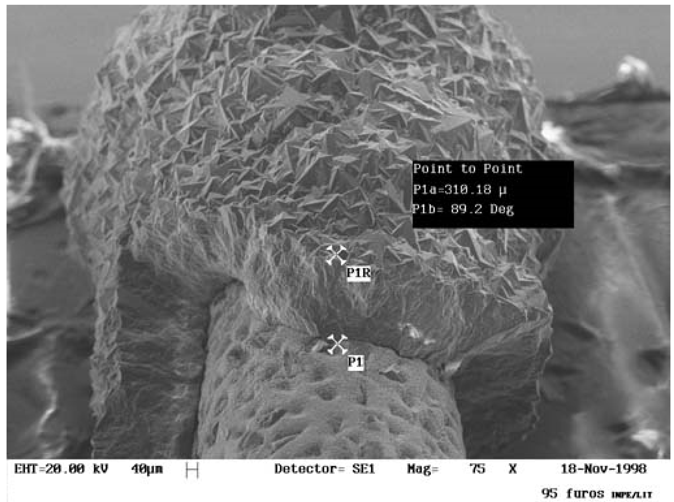
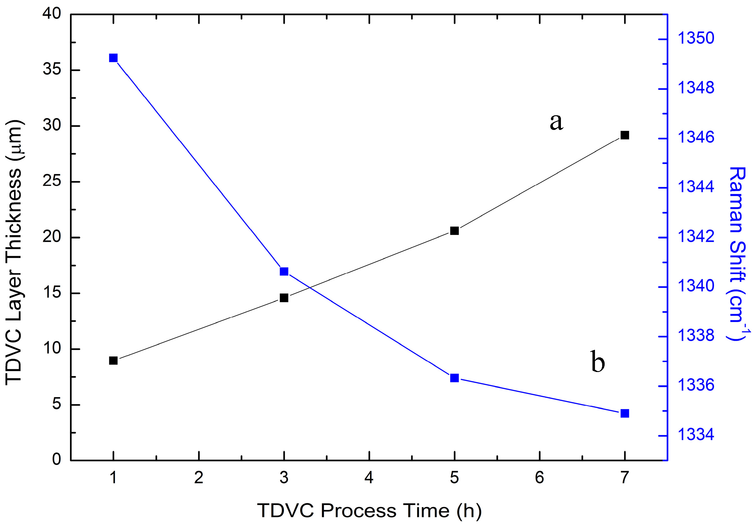
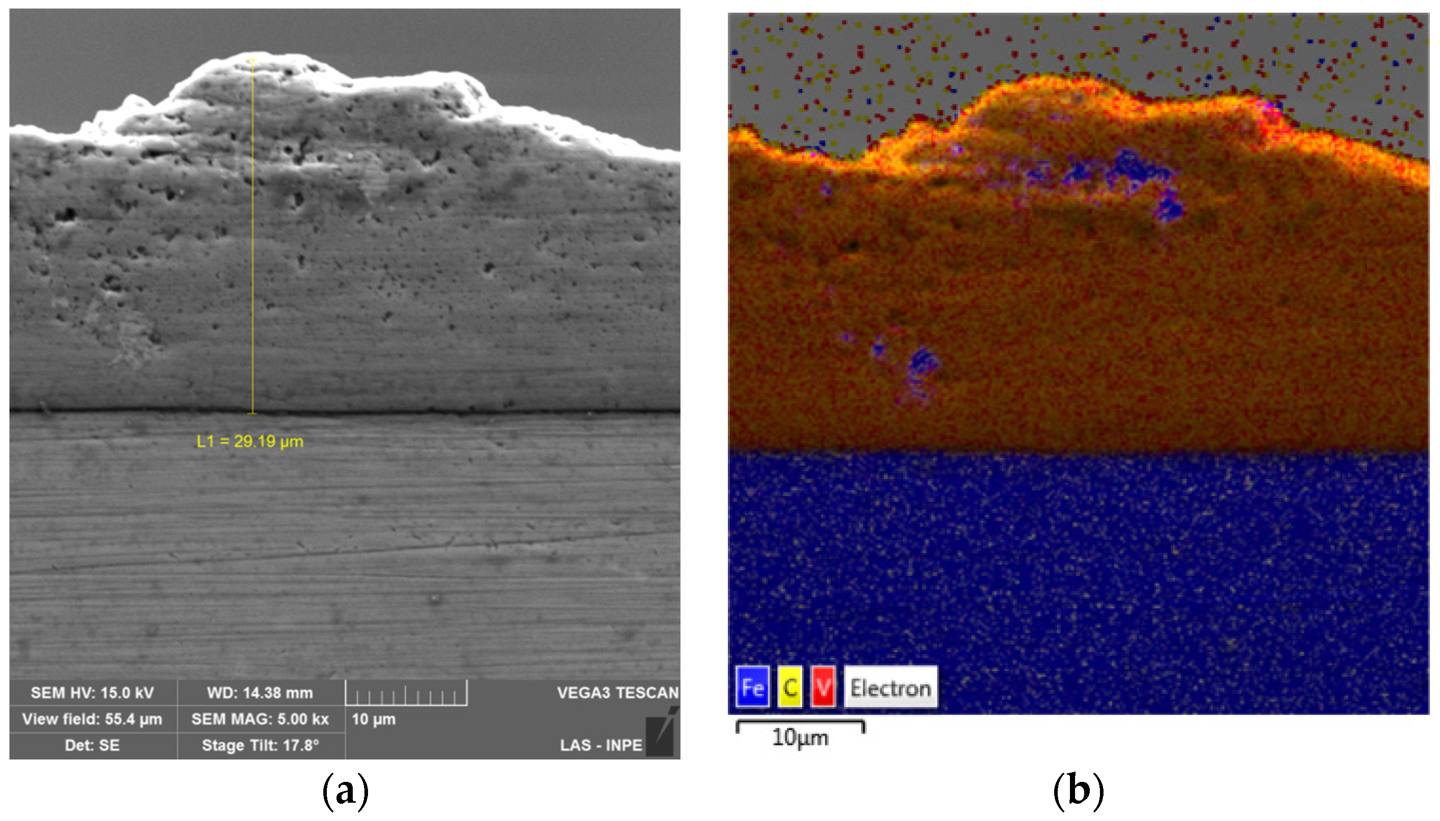
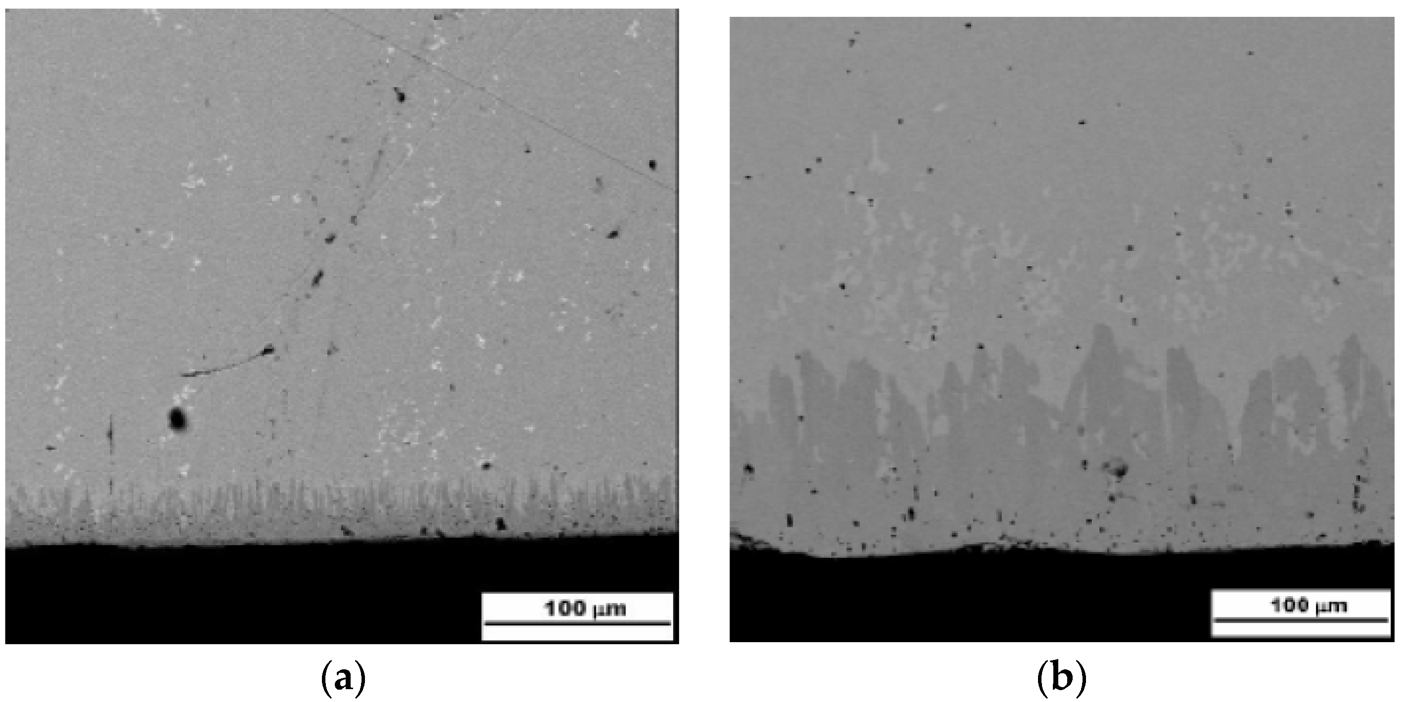
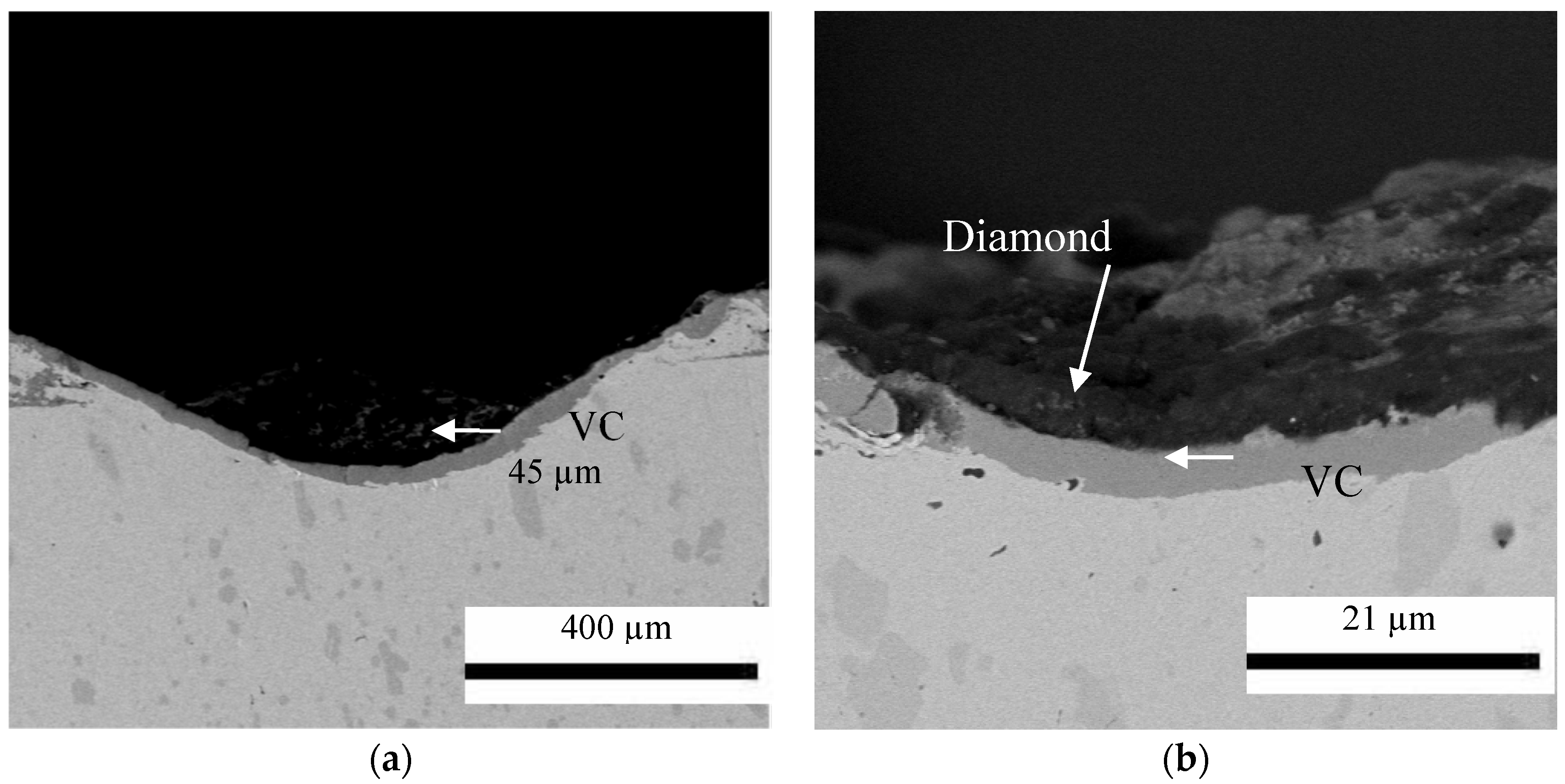
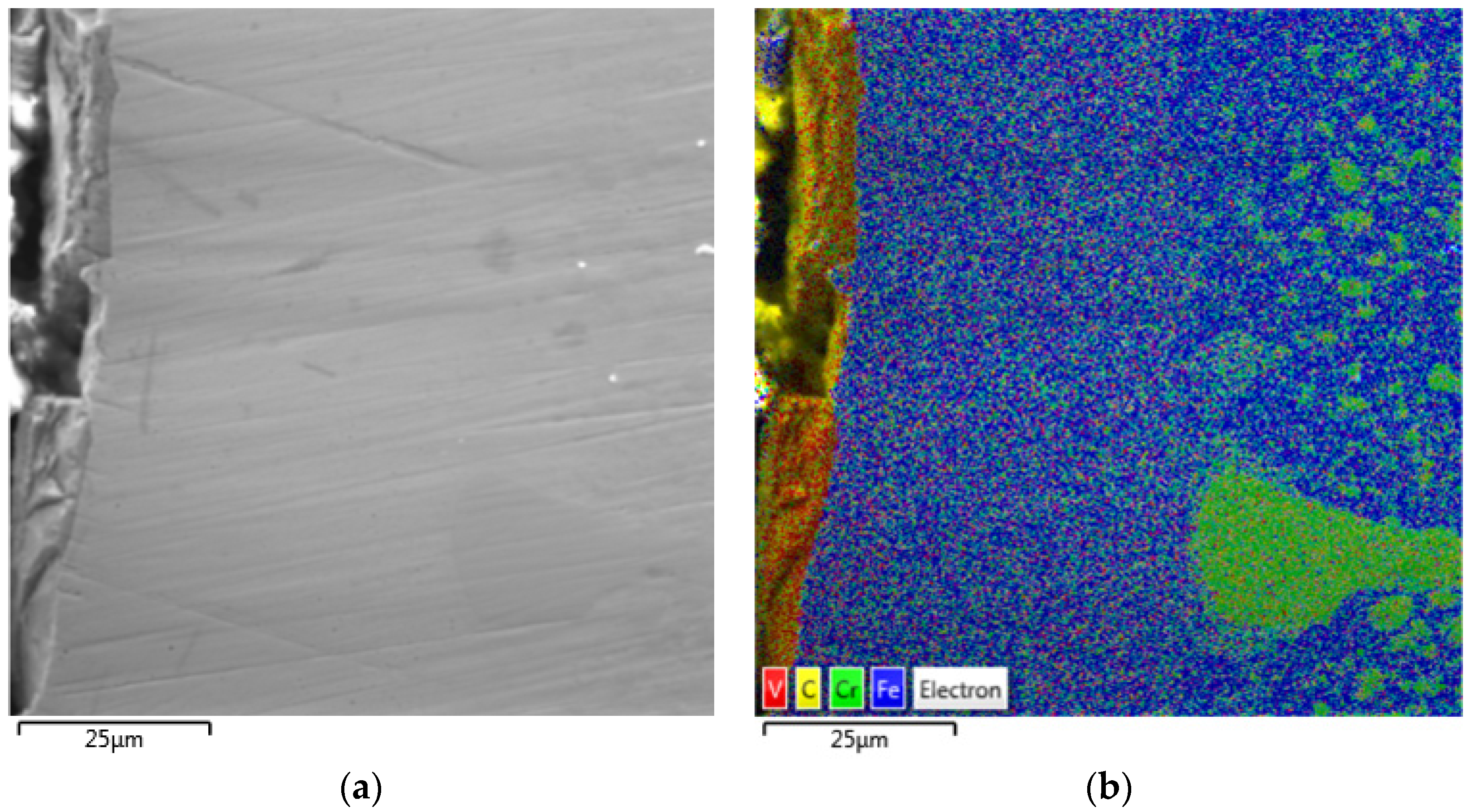
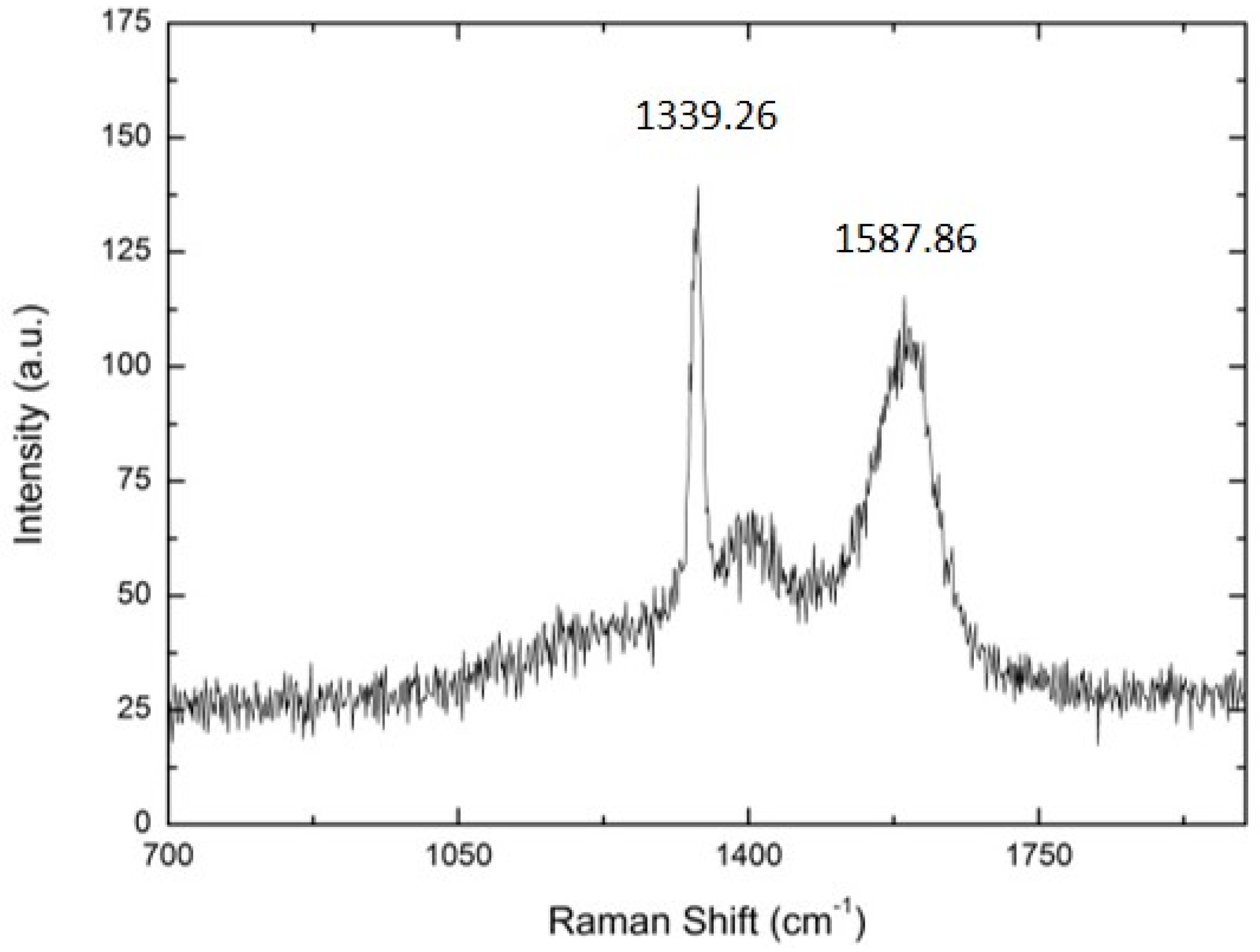
3.2. Thermodiffused Vanadium Carbide Coating (TDVC)
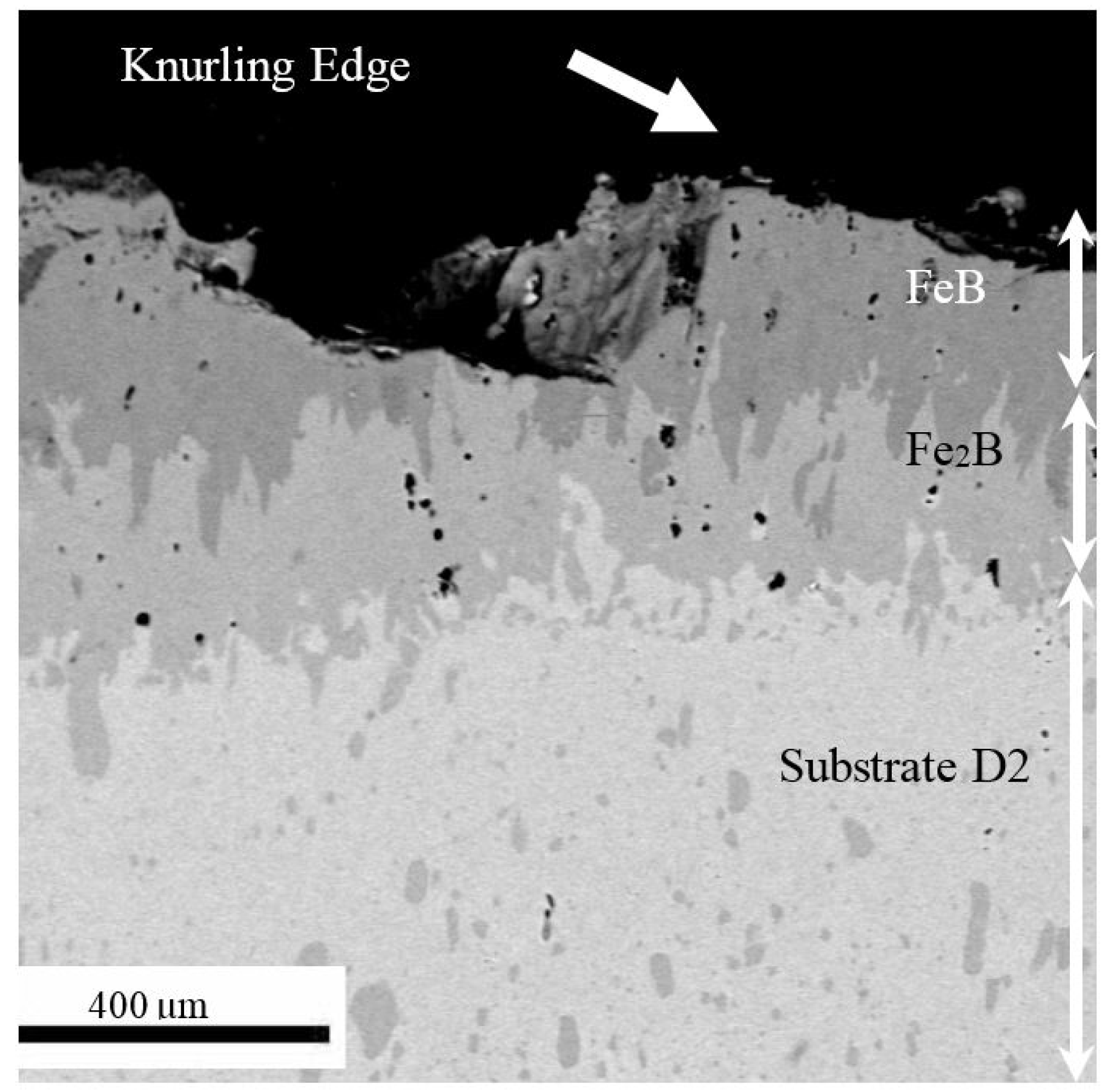
Barquete et al. [27,50] introduced the VC layer as a possible intermediate layer for diamond deposition on steel and WC–Co substrates. This first result showed cracks forming during the cooling stage from CVD diamond deposition temperature, typically 870 °C, for AISI D2 substrate. The Raman spectrum showed a huge compressive stress because of a double peak splitting with 20 cm−1 shift compared with natural diamond peak. The SEM image showed that the diamond film and VC intermediate layer were cracked but without any delamination. They commented on this remarkable stress level as evidence of TDVC feasibility as intermediate layers, because of mechanical strength and adherence. They also cited the intermediate value of the VC TEC, 6.06 × 10⁻⁶ K−1 at room temperature. All the results shown suggested VC as a good intermediate layer for CVD diamond growth. Raman spectra and the SEM images showed high quality diamond, suggesting the VC layer as an efficient carbon and iron diffusion barrier.
Thermodiffused vanadium carbide is a known industrial procedure for steel surface modification, called the Toyota thermodifusion process. The VC coatings have high adherence on steel substrates [51], hardness in the 1700–3150 HV range [52], high mechanical strength [53], high chemical resistance, and excellent wear resistance [27]. Besides being chemically compatible to grow CVD diamond films, VC has a convenient intermediate thermal expansion coefficient of 6.06 × 10⁻⁶ K−1 [54,55,56], lying midway between diamond and steel. These characteristics were important for selecting the TDVC coating as the intermediate layer for CVD diamond growth on steel substrates.
The TDVC process consists of a mixture of powders (Na2B4O7·10H2O (68 wt %) + V2O5 (24 wt %) + B4C (8 wt %)) placed within a crucible and heating to temperatures between 850 °C and 1050 °C [57]. In the salt bath, each reactant has a definite role. Vanadium pentoxide provides the metal forming (V or VC) [58]. Boron carbide is responsible for V2O5 reduction to V. Borax decreases the salt bath melting point and acts as an electrolyte to provide freedom for element migration, which makes the carbide reaction possible [59]. Carbon atoms diffuse from the steel bulk to the surface and react forming a dense and metallurgically bonded vanadium carbide (VC) [60].
Since the VC layer forms from carbon diffused from steel bulk, a good steel substrate for VC deposition requires a large carbon content. It is necessary to have at least 0.3% of carbon for VC layer formation on the metal surface [53].
Recently, we varied the thermodiffusion time in the range from 1 h to 7 h. In the first hour, there was a higher growth rate of 9 μm/h. For the following hours, the growth rate was close to linear. Figure 2a shows the VC thickness variation with thermodiffusion time. Diamond growth used a hot filament reactor at 50 Torr pressure, 700 °C substrate temperature, growth time of 3 h, 2 sccm methane (CH4) flow and 98 sccm hydrogen (H2) flow. Sample seeding with ultrasonic dispersion of 0.25 μm improved the diamond nucleation rate [61,62,63,64]. The HFCVD diamond film grown over the TDVC coating was continuous and homogeneous in all sample surfaces without cracks and delamination, even for the thinner VC intermediate layer. The crystals morphology showed a diamond grain size less than 1 μm. This diamond film had a 1.2 μm cross-section thickness. We evaluated the Raman shift position after diamond deposition on samples of different VC thicknesses. Figure 2b shows Raman shift dependence on thermodiffusion time and how it correlates to VC thickness. While VC thickness increases roughly linearly, the Raman shift decreases, probably limited to the TEC difference between VC and diamond. Note that 6.06 × 10⁻⁶ K−1 vanadium carbide TEC combined with 29.19 μm thickness could mitigate the diamond stress state reducing the Raman shift down to 1335 cm−1 [65]. VC is the first single intermediate layer to mitigate stress through thickening of an intermediate TEC material.
Figure 3a shows the SEM image of the thicker VC layer (29.19 μm). The mapping of Figure 3b shows the excellent separation between the steel substrate and the VC layer.

3.3. Iron Borides

Buijnsters [17] proposed the iron boride (FeB and Fe2B) intermediate layer for diamond deposition on steel. Borides are of great interest to modern technology because of their extreme hardness, durability, and resistance to acidic environment and to certain melting salts. The borides’ characteristic properties are associated with their crystalline structure and strong interatomic bonding. Boron atoms in the crystal structure usually form complex crosslinks and, covalent bonds between atoms have fundamental importance in borides [66].
The boride layer may consist of a single boride phase (Fe2B) or multiphase (FeB + Fe2B) [67]. Boron layer morphology, growth, and phases composition may depend on the alloying composition in steel. During boriding, boron atoms diffuse in steel with consequent interstitial formation of boron compounds [68]. The resulting layer has strong covalent bonds responsible for the high melting point, mechanical strength, and elasticity modulus [69]. However, applied as an intermediate layer for CVD diamond deposition, iron borides had the disadvantage of causing boride layer embrittlement [70]. Further, the FeB and Fe2B phases have different coefficients of thermal expansion (TEC), FeB = 23 × 10−6 K−1 and Fe2B = 7.85 × 10⁻⁶ K−1 [71], which may induce crack formation at the FeB/Fe2B interface. Control of powder composition, time, and temperature during pack boriding may favor the Fe2B phase over the FeB phase.
Buijnsters et al. [17] confirmed a two iron boride layer formation, FeB and Fe2B, with semi-spherical chromium boride precipitant. This boride intermediate layer favored high adhesion to the diamond film. The FeB presence on the surface resulted in a huge thermal stress. Despite the high residual compressive stress, Raman shift of 1354 cm−1, the film grown was continuous and homogeneous. Their best result was with Fe2B layer free of any FeB. They patented this method for CVD diamond deposition on steel [72].
Boriding is a thermochemical surface enrichment in which boron diffuses from the melting salt bath into the substrate. Independence on substrate carbon concentration is one of the boriding advantages. Boron carbide supplies the boron for thermodiffusion. A large SiC amount added prevents boron oxide formation and consumption because silicon oxide formation prevails over boron oxide formation. Potassium fluoroborate (KFB4) is an activating agent to lower the temperature for boron thermochemical diffusion [73]. Common carbon steels or alloy steels may be suitable. The thermochemical growth of multiphases relays on the boriding potential (depends on the B4C amount in the salt bath and on activation by KFB4) [7,8]. The substrate immersed in the boriding salt bath inside stainless-steel crucibles is fed to an oven at treatment temperatures from 800 °C to 1050 °C. Boride layer thickness depends strongly on boriding time, alloying in the steel, and temperature [74]. For example, at 900 °C, a SAE 1045 steel Fe2B layer becomes, in 4 h, 100 μm thick, 150 μm in 8 h, and 200 μm in 12 h [70].
Our group also studied steel boriding as an intermediate layer for CVD diamond deposition on steel substrates [74]. Generally, the mixtures of these powders were 82–85% of silicon carbide (SiC), 5–8% of boron carbide (B4C), 5% of potassium fluoroborate (KFB4), and 5% of alumina (Al2O3). We used the same proportions as Buijnsters et al. [17] to compare.
Thus, the boriding fundamental parameters are: temperature, the boron potential, and the activation energy. The boron potential is a parameter controlled by the boron availability in the powder mixture. The B4C and KFB4 concentrations control it. The activation energy depends only on the steel used. In general, a lower boron potential is necessary for steels with a lower activation energy. High-alloy steels are those with lower activation energy, AISI D2 steel was the lowest activation energy tested by us.
Tool steels, AISI D2 and M2, are characterized by their high mechanical properties and high percentage of carbon, even at high temperatures. In addition, a low alloy AISI 1020 steel study allowed comparison of steels with different activation energies for boride formation. Also in this same line, the SAE 52100 steel allowed comparison of a low alloy steel, but with a high carbon content.
With its low activation energy for boriding, the AISI D2 steel forms mainly FeB with difficult control of Fe2B growth [75]. Similar to AISI D2 steel, AISI M2 steel also presented a preferred FeB layer phase under the conditions proposed by Buijnsters [17]. However, only a Fe2B layer showed up with a mixing salt bath condition of: 1% of B4C, 5% of KFB4, 5% Al2O3, and 89% SiC.
With low alloy content and higher activation energy, the 1020 steel allowed greater control of FeB and Fe2B layer formation. The two distinct layers showed up at B4C concentrations above 5 wt %, in the mixture containing 5 wt % of KFB4, 5 wt % of Al2O3 and balanced by SiC. Differently from the D2 and M2 steels, where the boron layers were compact with a defined boundary line, the 1020 steel boride layer showed a dendritic arrangement with preferential growth into substrate without a definite boundary. This feature produced thick but irregular borate layers that may be of interest to improve the Fe2B layer adhesion to the substrate and decrease stress.
B4C concentration, reduced to 3%, formed purely Fe2B phase in the layer. B4C concentration in the mixture is predominant in shaping the boron layer composition. We showed Fe2B layer in AISI 1020 steel, grown for 30 min at 850 °C and 950 °C. Regardless of temperature, the FeB and/or Fe2B phase deposition depended only on B4C concentration. The temperature affected only the growth rate.
The SAE 52100 steel has the following composition by weight: 1.21% C, 0.20 Cr, 0.10% V, 1.0% W, and 0.25% Mn. The boriding mixture changed for SAE 52100 steel to mitigate a significant carbon loss from the substrate to the salt bath. We replaced alumina by graphite in the boriding mixture. Therefore, the powder mixture took on the following composition: 1–5% of B4C, 5% of KFB4, 5% of graphite, and 85–89% of SiC. Figure 4 shows the backscattered electron micrograph of the SAE 52100 steel borided at different processing times, at a temperature of 950 °C. This shows the total control of Fe2B layer formation at the chosen thickness.
We performed diamond film growth on specimens covered with borides in a Hot Filament reactor (HFCVD) at 50 Torr pressure, 700 °C substrate temperature, growth time of 3 h, 2 sccm methane (CH4) flow and 98 sccm hydrogen (H2) flow. In the AISI D2 steel, which always had a FeB phase layer, the diamond grown had excellent quality but delaminated from the surface because of its large thermal expansion coefficient. The AISI M2, AISI 1020n and SAE 52100 steels covered by FeB phase had the same result: delaminated high-quality diamond. An example of diamond deposition on the FeB layer is shown in Figure 5. The delaminated parts showed excellent diamond film, as characterized by the Raman spectrum of Figure 5a. The parts that remained adhered to the substrate showed a large displacement of Raman shift, 1347.5 cm−1, which confirmed a high compressive stress of 8.75 GPa.
The diamond deposition on the Fe2B layer showed the characteristic peak of diamond with reduced compressive stress at 1336 cm −1. However, its low intensity and high amorphous carbon content shown by the 1580 cm−1 Raman band illustrated its poor quality.
From this set of diamond deposition results on boron layers we concluded, as Buijnsters, that the FeB layer is an efficient diffusion barrier for iron effects on the diamond growth, but does not solve the high thermal stress problem. Contrasting, deposition on Fe2B solved the TEC problem, but it clearly is not an efficient diffusion barrier.

3.4. Multilayers with Fe2B to Mitigate Thermal Stress

The good result with Fe2B in mitigating thermal stress induced research on ways to block diffusion efficiently by a second layer deposition over the Fe2B layer. We tried controlled growth of a thin FeB layer and a VC layer, both by thermo-reactive processes [74]. Results were better than only with Fe2B, but still limited. This alternative could be tested with other second intermediate layers able to block carbon and iron diffusion.

3.4.1. The Multilayer of Fe2B with a Controlled Thin FeB Layer

The first layer was deposited on the steel substrate consisted of a thick Fe2B phase aiming to minimize the thermal stress. On top, there was a thin FeB layer to block carbon diffusion into substrate. AISI M2 and AISI 1020 steels were used because of better boride phase control. This is different from the normal growth of both phases in low activation energy steel, because there is complete control of each phase’s thickness. Figure 6 shows an example of both films grown on AISI 1020 steel.
For comparison, boride layers were grown on both steels (AISI M2 and AISI 1020) for different times: Fe2B growth for 4 h; Fe2B for 4 h, and subsequent FeB growth for 0.25 h, Fe2B for 4 h, and subsequent FeB growth for 0.5 h. Diamond growth on these samples followed in the HFCVD reactor with the following parameters: 1–2% of CH4; total flux of 100 sccm; 50 torr; work distance of 3 mm; substrate temperature at 650–850 °C; and deposition time of 3 h. The Raman spectrum in Figure 7 shows the CVD diamond stress and quality on these boride layers.
The Raman spectrum of the film grown on 1020 steel, with only the Fe2B layer, is characteristic of an amorphous carbon film, without a diamond peak. The FeB layer formation for 15 min in the second boriding stage improves substantially the grown diamond, showing up the characteristic diamond peak at 1333 cm−1. In the M2 steel, only with the Fe2B layer, can we see the diamond peak at 1333 cm−1, superimposed on the amorphous carbon characteristic bands. Forming the FeB layer, in the second boride stage, a significant improvement in diamond film quality is noted, which is progressive with the increase of the FeB layer. Comparing the results using only the Fe2B phase as intermediate layer, better diamond quality was shown on the AISI M2 substrate, because the high alloy content in this matrix formed a more compact Fe2B phase.
On the other hand, the quality improvement comes with a greater displacement of diamond peak position, to the region of 1336 cm−1, pointing out an increase in the thermal stresses. These experiments showed that two-step boriding was efficient in reducing thermal stresses and improving diffusion barrier characteristics. Diffusion barrier improvement was gradual with the increase of the FeB layer thickness. The results for the 1020 and M2 steels seemed to be the limit for diamond film quality improvement by this alternative. Further increasing FeB thickness raises the thermal stress and the diamond film may delaminate spontaneously on cooling after deposition.

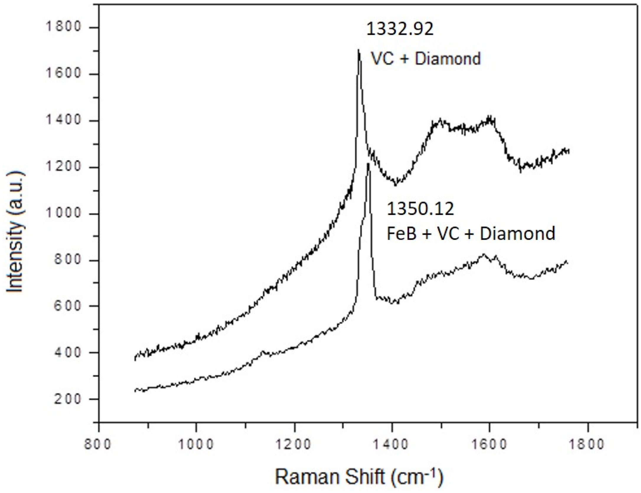
3.4.2. The Multilayer of Fe2B with Vanadium Carbide Layer

The Fe2B layer does not effectively block the carbon diffusion into the steel substrate. Then, it also does not block carbon diffusion from the steel substrate to the surface. This could enable VC growth by the TDVC described in Section 3.2, on top of the Fe2B layer. To test this alternative the SAE 52100 steel was chosen as substrate. It is a low alloy steel, which enables controlled Fe2B growth, and has enough carbon content for VC growth on the surface [74].
The Fe2B layer could not fully prevent carbon diffusion from the interior of the substrate and the VC layer formed on the surface during reactive thermodiffusion. However, the TDVC salt bath interacts with the boride layer partially removing it. Steels with less than 30 min of Fe2B boriding time form a thick and rough VC layer, with complete disappearance of the Fe2B layer, as if the VC film had deposited directly on the SAE 52100 steel substrate. This shows Fe2B phase instability in vanadium carbide thermodiffusion conditions. In the samples borided for 60 and 120 min, the boride layer rearranges but the VC layer deposits on top of it. It indicates that VC layer deposition occurs by carbon diffusion through the Fe2B layer. In fact, this reaffirms the inefficient diffusional barrier built by the Fe2B coating.
Figure 8 shows the diamond film grown at the same conditions as in Section 3.4.1 on the sample with Fe2B growth for 2 h and VC growth for 4 h. The SEM image of Figure 8a shows a delaminated diamond film with only small parts remaining adhered to the substrate. The Raman spectrum of Figure 8b, acquired from this adhered diamond pieces, show good diamond quality and Raman shift of 1335 cm−1. This small stress may indicate efficient stress relief by this multilayer. However, the delamination shows low adherence to this VC surface. The Fe2B instability in the VC growth condition and carbon diffusion through the Fe2B layer probably resulted in a VC phase that is not satisfactory for CVD diamond adherence.

3.5. Mechanical Interlocking Applied to Relief Residual Stresses in Highly Stressed Diamond Films

A great challenge is to minimize the thermal stresses produced during cooling after diamond growth on steel. VC and FeB layers showed best results as diffusion barriers. However, thermal stress relaxation because of large differences in TEC between steel and diamond is difficult. In both cases, on smooth substrates, it was common to see spontaneous diamond delamination upon cooling. When adhered, the Raman spectra show a high stress state, which points to high adhesion forces. The same is true for most intermediate layers found in the literature.
However, the problems of FeB and VC intermediate layers are clearly different. The FeB easily grows thick layers but it presents a TEC even higher than steel substrate. VC has intermediate TEC but its growth to thicker layers to relax residual thermal stresses is not always easy.
An alternative to promote residual stress relaxation is mechanical interlocking on uneven surfaces [74]. To promote the mechanical interlocking, we opted for laser knurling on the surface. The laser knurling produced a symmetrical cross scratching with 100 μm spacing and 60 μm depth. The samples were AISI D2 steel. As shown before, this is a steel in which the FeB layer grows easily and VC thickening is hard, both caused by the high chromium alloying.
In this section, we present a comparative study of mechanical interlocking effects. We tested residual stress relaxation by laser knurling on steel substrate coated with FeB and VC layers. However, the laser knurling relaxation method could help other intermediate layers.
Knurled samples were borided in a mixture containing 1% by weight B4C, for 4 h at 950 °C. Figure 9 shows cross section SEM backscattering images of knurled and borided D2 steel. It shows the diffuse layers of the Fe2B phase covered by the FeB phase.
The boriding into knurling valleys was shown to be less efficient with a smaller FeB phase thickness. Probably the solid powder salt bath did not fill the valley regions. The Fe2B layer shown on the surface was not desired because of a decrease in diamond film quality. Despite several attempts, no diamond film remained on top of this intermediate layer. Spontaneous delamination always occurred on cooling down of the reactor. It is evident that high TEC material, as FeB, is not suitable even for this highly knurled surface.
The diamond deposition, made at the same conditions as in Section 3.4.1, was successful on laser knurled substrates with two types of intermediate layers: multilayer of FeB + VC; and only VC layer. Figure 10 shows the SEM images of the cross sections of VC layer on a knurled steel surface.
After the vanadium carbide growth, a redistribution of the boron layer occurred, the Fe2B phase disappeared, forming only the FeB layer and a thin and poorly homogeneous VC layer. This result shows, as expected, that the FeB phase partially inhibits VC layer formation because of efficient blocking of carbon diffusion from the substrate. The Fe2B phase is less stable to heat treatment during VC deposition. The surface available for CVD diamond deposition was FeB with VC islands, but a homogeneous CVD diamond film deposited on the sample surface.
For samples only with VC deposition a homogeneous VC layer formed, even inside the valley regions (Figure 10a). The salt bath is liquid at the TDVC temperature and wets even the valley regions. Diamond deposition on the VC resulted in a homogeneous and continuous film (Figure 10b).
The diamond films deposited had their state of residual thermal stress altered by laser knurling. There was no diamond spontaneous delamination from any sample, as noted in the ones not knurled with the same intermediate layers. A more detailed study of the residual stresses by Raman spectroscopy shows significant differences in the two types of intermediate layers.
Figure 11 shows the Raman spectra of diamond film deposited on knurled AISI D2 samples with VC and with FeB + VC intermediate layers, respectively. For the samples with only a VC intermediate layer the thermal stress is substantially relieved, since the Raman shift is around 1333 cm−1. However, the result with the FeB + VC layer is unsatisfactory since the residual stresses remained huge, as noted by the Raman shift close to 1350 cm−1.
Diamond film adhesion to these substrates is a compromise between the adhesion force and the tension state. Since spontaneous delamination occurs without laser knurling in both types of substrate, the first test was a non-aggressive one: the adhesive tape test. We used standard ASTM D 4080 [76] in the D2 steel samples to verify adhesion of the intermediate layer and diamond film. Diamond delaminated from the knurl crest for samples with FeB + VC intermediate layer, but nothing happened in the samples with VC intermediate layer. Thermal stress decrease obtained by laser knurling and the VC layer were enough to improve the diamond film adhesion in the adhesive tape test level.
To better study the diamond film adhesion in these samples, we used indentation tests in a Rockwell hardness tester, using the Rockwell C tip with different penetration loads: 20, 30, and 40 kgf. All the samples presented delamination around the indentation region, but, clearly, the samples with FeB + VC layer presented a larger delamination area, extending to several knurl periods. The number of knurl periods involved in the delamination increased with the applied load. For samples with VC layer, delamination remained delimited to a single knurl period, around the indentation point, regardless of the applied load. Therefore, the vanadium carbide treatment used as intermediate layer showed much better resistance to penetration and delamination.
This set of results on laser knurling for residual stress relief showed two distinct circumstances. With the FeB + VC layer the residual stress decrease was unsatisfactory, as shown by the Raman spectra and the always negative results of adhesion tests. With the VC layer, the residual stress decrease was effective, substantially improving the diamond film adhesion. The significant difference witnessed in knurled substrates shows that lower VC TEC is essential for efficient stress relief by mechanical interlocking, even for a relatively small VC thickness. The result with the FeB + VC layer shows that mechanical interlocking alone is not enough for effective residual stress relief for high TEC materials.

3.6. Chromium Carbides

Chromium is widely used in steel alloying. Chromium presence increases the steel resistance against oxidation at high temperatures [77], fills the empty spaces in the structure [78], reduces porosity on the surface [79], and is a good carbide former [80]. Chromium carbide produces high hardness of 1750–2740 HV on the material surface, and has a low friction coefficient (0.47–0.65) [81]. Chromium carbide also has a thermal expansion coefficient of 10.4 × 10⁻⁶ K−1 [82].
Schwarz et al. [83] developed a chromium carbide intermediate coating produced by diffusion onto surfaces of 41Cr4 steel rings. The chromium diffusion consisted of mixtures of Cr-powder (99.8%) in vacuum (p = 1.33 at 10−2 Pa) at 1100 °C for around 6 h. A chromium carbide layer formed on the substrate surface because of reaction between Cr and the carbon diffused from substrate. The chromium carbide layer was 10–12 μm thick, because of a growth rate of 1.67–2 μm/h. The chromium carbide phase formed was Cr23C6.
Schwarz et al. deposited diamond on Cr23C6 in an industrial hot-filament plant set at 10 mbar, 1% of CH4, 1000 sccm gas flow, substrate temperature of 900 °C, work distance at 20 mm, and 10 h of deposition time. The diamond grown was a homogeneous 1.6 μm thick film. The XRD diffractogram showed a Cr2C3 phase after diamond deposition. Enrichment in carbide phase occurs because of the high carbon reactivity in the gas phase during HFCVD deposition. The in place Cr2C3 phase formation on the material surface makes diamond covalent bonding to the substrate and improves its adhesion [83]. The Raman shift was 1341 cm−1, representing a 5.1 GPa compressive residual stress. The Raman spectrum also shows a large amorphous carbon content in diamond film.
Bareiß et al. [84] developed a similar and very important work by using chromium carbide as intermediate layer. Substrates were the 41Cr4, X46Cr13, and X50CrMoV15 steels. They performed chromizing diffusion with Cr-powder medium (99.8%); at p = 10−2 mbar, temperature at 1150 °C, and for 4 h. The chromium carbide Cr23C6 phase was 20–25 μm thick, by a higher deposition efficiency (5–6.25 μm/h) compared with the Schwarz work. The chromium carbide diffusional barrier is more efficient against iron migration from the substrate than carbon diffusion [85].
As in the Schwarz paper the carbon diffusion from the diamond growth gas phase changed the chromium carbide phase. The phases Cr7C3 and Cr3C2 appeared in the XRD diffractogram. Kellerman et al. also showed that the original Cr23C6 phase keeps the diamond adhered and it delaminates from the Cr7C3 and Cr3C2 phases. Their work set up a new principle for stress relief: the growth of the CVD diamond above the steel phase transformation temperature. During heating above 750 °C the steel changes its cellular organization from ferritic bcc to austenitic fcc ending its linear expansion. The CVD diamond growth over austenitic fcc phase followed by a slow cooling makes the steel expand to become ferritic bcc phase again and it can promote a compressive stress decrease in the HFCVD diamond [86].
Bareiß et al. deposited a homogeneous 1.5 μm thick diamond film. The diamond growth conditions were pressure of 10 mbar, 1% of CH4, 1000 sccm gas flow, substrate temperature of 850 °C, and 6 to 10 h of deposition time. Because of TEC mismatch they obtained a high 8.7 GPa compressive stress [84] calculated from the Raman shift at 1352 cm−1 [87]. Despite this good attempt, probably the high chromium carbide TEC is still responsible for the high thermal residual stresses.
The control of the chromium carbide phase on the surface after CVD diamond growth turns out to be the key subject in forming these intermediate layers. Chromium nitride intermediate layers have also shown the same problem, since chromium nitride becomes chromium carbide after CVD diamond growth. As Bareiß et al. [84] and Kellerman et al. [86] have shown this phase control is fundamental. A good guide to obtain such control is the work of Degutis et al. [88] that verified chromium carbide layer reaction during CVD diamond growth.

3.7. Laser Cladding

Contin et al. reported the newest method to interpose an intermediate layer for CVD diamond growth on steel: laser cladding [28]. The laser cladding produces surface modification by transformation hardening and remelting. It creates a dense coating, with laser irradiation on a powder spread on the substrate surface to promote a strong metallurgical bond [89]. The advantages of laser cladding over conventional techniques to create a diffusion barrier include a faster processing speed, high heating/cooling rate, precision, automation, and versatility. The main advantage is not affecting the material bulk properties, which is good for high performance cutting tool development. The main disadvantage is deposition in the laser line of sight, which may be a problem for three-dimensional samples. The surface melting leads to different microstructures in the deposited layers, which mainly depend on the powder elements and on the laser process parameters. The extremely high cooling and solidification rates cause fast re-solidification that may lead to crack formation. This is a significant disadvantage because of the possible inherently brittle nature of the microstructures formed. Further, laser cladding is a mature technology, a complete apparatus with automatic powder feeding, laser control, and several axis CNC machines are available. The laser scans are always focused at the powder surface. Powder and substrate melt to form molten pools, which solidify into fully dense metal layers after the laser focal spot moves away [90]. Laser fluence manages the local surface heating, which enables full control from full surface melting to moderate heating to promote controlled sintering. Successful laser surface alloying has been carried out experimentally for a variety of substrates and alloying elements [91].

3.7.1. Laser Cladding of SiC Layers

In this pioneering work, with silicon carbide, Contin et al. used a two-step procedure (pre-placed laser cladding). The powder to create the intermediate barrier was a commercially available silicon carbide powder (Treibacher Schleifmittel Brasil) with predominance of rhombohedral crystal and average grain size of 4 μm. The first step consists of powder application by an air gun of a mixture of 25 g of SiC and 1 g of carboxymethylcellulose (CMC) in 120 mL of ethanol. The second step is laser treatment by a CO2 laser with wavelength of 10.6 μm. These two steps applied once formed a single SiC layer. Both steps repeated for three and six times created 3- and 6-layers of SiC. Each laser irradiation (12.7 mm diameter samples) took only 10 s. Laser fluence was high enough to locally melt the AISI 304 austenitic stainless-steel surface, but not to melt or decompose the SiC particles.
The single SiC layer showed complete SiC decomposition inside the substrate molten pool to form a FeSi phase after substrate cooling. These FeSi layer showed diffusion barrier properties, since CVD diamond grew well on these single-layer SiC samples. Buijnsters [19] had already shown FeSi potential as a diffusion barrier, but laser cladding promoted silicon diffusion to up to 30 μm into stainless-steel, enabling good quality diamond growth. This single SiC intermediate layer could not relieve the high thermal stress between the stainless-steel (TEC of 17 × 10−6 K−1) and diamond. However, applying the conventional alternative: growing nanocrystalline diamond (NCD) at low temperature (550 °C) and only 200 nm thick produced an adherent film with a good diamond quality and a Raman shift around 1350 cm−1, as shown in the Raman spectrum of Figure 12. This result is impressive because the TEC of stainless steel is much higher. Literature shows only a few experiments without diamond film full delamination from stainless steel, as the experiments of Buijnster et al. with Fe2B [17] and CrN [33] intermediate layers.
The idea of depositing three and six SiC layers was to improve stress relief by a thick SiC layer. After each layer deposition, the surface material and properties change. This changes the thermal and laser interaction properties for the next layer. Up to the 3-layer samples, iron continues to migrate among SiC particles to form the prevalent FeSi phases, but some unreacted SiC phase is now present. The surface morphology resembled uniform and smooth sintering, probably with iron flowing around SiC particles and serving as binder. Up to three layers there was enough heat transfer to mix up some molten iron among the SiC layers and to form a FeSi binder. The SiC diffusion up to around 30 μm shows that the first layer deposited the same diffusion barrier shown for the single layer samples. The total layer thickness was around 12 μm. Rockwell A. indentation tests on 3-layer SiC samples showed a rough surface. Diamond growth on these samples shows excellent quality diamond films adhered to the substrate and a Raman shift of 1334 cm−1. The stress relief noticed correlated to the intermediate layer properties but it probably has a contribution from mechanical interlocking, since the relatively rough surface results from the laser cladding of 3-layer SiC. XRD from the 3-layer SiC samples after diamond growth shows some reactivity with the gas phase. FeSi phase continued to be prevalent, but there was some reaction with carbon to form the intermediary Fe1.34Si0.66 and Fe1.92C0.08 phases.
For the 6-layer SiC samples, surface morphology showed partially sintered SiC particles with a fragile appearance, as confirmed by Rockwell A. indentation. Silicon carbide was the prevalent phase and there was some FeSi phase. The remaining iron close to the surface did not turn out to be an efficient binder. Diamond grown on this rougher surface showed excellent characteristics, but intermediate layer fragility precluded any applicability.
Contin et al. [28] deduced that SiC layers deposited by laser cladding fulfilled the conditions for diamond deposition on ferrous substrates. The coating showed good metallurgical bonding with steel and led to a good diffusion barrier. This barrier avoided graphitic formation. The layers proved to be also effective in limiting carbon diffusion during diamond deposition. Results suggested FeSi, formed by SiC dissociation, as the main reason for diffusion barrier effectiveness. Further layers, 3- and 6-layer SiC, efficiently relaxed the high thermal stress produced by the enormous difference between stainless-steel and diamond TEC. However, it became clear there was a need for a binder for SiC particles to produce tougher layers. Iron became such a binder to a certain extent.
These authors, taking advantage of laser cladding versatility to change and mix powder materials, continued the research to include titanium and copper powder mixed with SiC [89]. Titanium inclusion formed a new phase with iron and silicon, that is even better than FeSi as a diffusion barrier. Better quality diamond grows with a shortened incubation period, on single Ti and single SiC layers cladded on stainless steel. Copper mixtures with SiC resulted in nicely sintered coatings.

3.7.2. Laser Cladding of VC Layers (LCVC)

The success with thermodiffused VC layers and the success in laser cladding application induced our group to study laser cladding of VC layers [29]. If we could reproduce the benefits of the VC intermediate layer for diamond deposition on steel, but take advantage of laser cladding versatility, we could remove the limits of VC thermodiffusion only to high carbon content and low alloy steels. This subsection shows the preliminary data in this research.
In VC layer processing by laser cladding, chromium is not negative to layer formation as for the thermodiffused film. In addition, chromium helps to protect the uncoated surfaces against corrosion [79,92] and it is important to increase the cutting tools’ life. Laser cladding changes only the material surface, keeping the bulk integrity. We selected AISI D6 steel because of its composition, with a high percentage of carbon and chromium. In these experiments, we used commercially available (99% pure) vanadium carbide spread on the substrate surface. The VC powder absorbed the laser energy and melted the steel surface forming a liquid phase while vanadium and carbon went through a molten pool.
VC powder bought from Chengdu Best New Materials had average particle size of 10 μm. The substrates were disks (18 mm diameter × 4 mm height) cut from AISI D6 steel round bars, sanded with up to 600 mesh sandpaper and cleaned in an acetone ultrasonic bath.
The laser beam parameters for construction of the LCVC layer were: resolution 300, 600, and 900 dpi; scanning speed 100, 300, and 500 mm/s and only one heating cycle. The laser used was a Synrad-SH with output power of 125 W and beam diameter of 180 μm. Beam intensity was 400 kW/cm2 and nitrogen flow purging avoided sample surface oxidation. Best conditions were VC film grown with 600 DPI resolution and 100 mm/s scan speed. The vanadium carbide film deposited by laser cladding was rougher than the TDVC one, with Ra = 1.48 μm, Rq = 1.83 μm and Rz = 6.66 μm.
Figure 13 shows the AISI D6 cross-section and the LCVC coating. The LCVC coating had a 6 μm thick cross-section. The energy dispersive spectroscopy (EDS) mapping analysis shows chromium distribution from surface to inner substrate in an extended heat affected zone (HAZ). The HAZ area was the region found between the LCVC interface and the substrate. The HAZ depth could be correlated to laser beam speed and resolution. The chromium from the bulk dissociated and homogeneously spread along the HAZ and the LCVC coating (Figure 13b). The HAZ presented a uniform chromium distribution. Further, chromium concentration increases in the LCVC coating because of its diffusibility in the melting pool. Chromium spreading through the coating and substrate contributed to increase the LCVC coating metallurgical bonding to the substrate.
Diamond growth on the LCVC intermediate layer resulted in film delamination and cracking. For the diamond pieces left on the surface the diamond morphology showed good quality faceted grains and, the Raman spectrum (Figure 14) showed a Raman shift of 1339 cm−1. The high compressive stress promoted delamination, but the pieces left on the surface were still stressed, meaning that adherence was high. This result was like a VC film of equivalent thickness grown by thermodiffusion.
Much work is still necessary to solve the many problems of LCVC film formation, such as avoiding film cracking and increasing its thickness to help thermal stress mitigation for diamond deposition. However, this preliminary experiment showed good perspectives to the LCVC alternative.

4. Concluding Remarks and Perspectives

CVD diamond deposition on steel substrates has been long expected. The technological importance of these substrates justifies this expectancy because of the many applications as machining tools, conformation tools or tribological surfaces. Research on this difficult problem has evolved to a great extent for almost 30 years. There are several intermediate layers that allow CVD diamond deposition on steel, but only a few alternatives have managed to solve the thermal stress problem. The huge stress developed at the interface because of high mismatch in thermal expansion coefficients limits applicability, despite the high adherences remarked. We focused this review on a few alternatives, mainly the ones in which our group has been working on for more than ten years.
At first, the multilayer alternatives seemed natural to mitigate thermal stress. Despite the relative success in depositing thick unstressed diamond films, these multilayers revealed other fragilities, as low adherence or softness of some of the intermediate layers, which limits application.
Our group proposed the thermodiffused VC layer and continued its development for several years. Recently the VC intermediate layer has shown to be the most promising one. It is the first single layer that has an intermediate thermal expansion coefficient and could be grown to a thickness large enough to mitigate thermal stress. Despite being a disruptive result that may enable many applications, it is limited to high carbon content and low alloying steel substrates.
The boride intermediate layer proposed by Buijnsters et al. [17] is a great solution, but poor diamond quality and only moderate adherence are still unsolved issues. The main reason for these problems is the only partial blocking of the carbon diffusion. We proposed the Fe2B layer only to mitigate thermal stress, because Fe2B has an intermediate thermal expansion coefficient and easily grows thick layers, but with an extra layer as a diffusion barrier. We tested thin FeB layers (grown for short time) and VC layers. The results were promising. Probably other layers studied in the literature could provide even better results. Perhaps aluminum or titanium layers are the best candidates.
Mechanical interlocking is a long-recognized method to relieve stress. Results show up successful only for the right intermediate layer. In this case, only an intermediate layer with an intermediate thermal expansion coefficient gave good results. A relatively thin VC layer combined with laser patterned mechanical interlocking gave excellent CVD diamond adherence to steel substrate, with low stress. For example, abrasive tools could promptly take advantage of these results. On the other hand, an intermediate layer with a high thermal expansion coefficient is not a solution even for laser patterned surfaces. This was true for the FeB intermediate layer, but CrN or other relatively high thermal expansion coefficient materials probably would also give only partial stress relief.
Laser cladding is a new method to interpose an intermediate layer, which expands the possibilities by including depositions from different powders, including ceramic ones. It already has shown great potential to produce excellent diffusion barriers as the FeSi and VC layers already shown. This method may form many other unusual diffusion barriers. Further, laser cladding opens the opportunity for thickening the intermediate layer with a dense sintered structure, as shown for SiC either with iron or copper binders. Laser cladding development in this area is still in its infancy, but perspectives are worthy.
Lastly, each of the main methods described has its advantages and disadvantages for application. Pack boriding and vanadization are conventional industrial processes with vast experience of scaled production. Both are high temperature processes in a relatively harsh environment, but their applicability is proven. Both are cost effective because of the use of large ovens to process several samples in a single salt bath, to compensate for the long process time. Both can deposit on 3D surfaces. However, a vanadization salt bath is a liquid and wets out better small surface details, as shown by the knurled surfaces in Section 3.5. Laser cladding, on the other hand, treats piece by piece in a few seconds. Its main disadvantage is the higher investment to have a laser coupled to a multiple axis machine to allow 3D surface treatment, since it is a line of sight method.

Acknowledgments

The authors wish to acknowledge support from FAPESP (2012/15857-1, 2013/25939-8, and 20015/25149-2) and FAPESB/CAPES (edital 017/2015). We also acknowledge the Federal University of São Paulo (UNIFESP), the National Institute for Space Research (INPE) and Associated Laboratory of Sensors and Materials (LAS) for supporting this scientific research.

Conflicts of Interest

The authors declare no conflict of interest.

References

  1. Matsumoto, S.; Sato, Y.; Tsutsumi, M.; Setaka, N. Growth of diamond particles from methane-hydrogen gas. J. Mater. Sci. 1982, 17, 3106–3112. [Google Scholar] [CrossRef]
  2. Badzian, A.; Badzian, T. Diamond homoepitaxy by chemical vapor deposition. Diam. Relat. Mater. 1993, 2, 147–157. [Google Scholar] [CrossRef]
  3. Lee, S.-T.; Lin, Z.; Jiang, X. CVD diamond films: Nucleation and growth. Mater. Sci. Eng. R Rep. 1999, 25, 123–154. [Google Scholar] [CrossRef]
  4. Kobashi, K. Diamond-structure and CVD growth. In Diamond Films; Elsevier: Amsterdam, The Netherlands, 2005. [Google Scholar]
  5. Miranzo, P.; Osendi, M.I.; Garcia, E.; Fernandes, A.J.S.; Silva, V.A.; Costa, F.M.; Silva, R.F. Thermal conductivity enhancement in cutting tools by chemical vapor deposition diamond coating. Diam. Relat. Mater. 2002, 11, 703–707. [Google Scholar] [CrossRef]
  6. Campos, R.A.; Contin, A.; Trava-Airoldi, V.J.; Moro, J.R.; Barquete, D.M.; Corat, E.J. CVD Diamond Films Growth on Silicon Nitride Inserts (Si3N4) with High Nucleation Density by Functionalization Seeding. Mater. Sci. Forum 2012, 727–728, 1433–1438. [Google Scholar] [CrossRef]
  7. Ying, Y.; Ying, W.; Li, Q.; Meng, D.; Ren, G.; Yan, R.; Peng, X. Recent advances of nanomaterial-based membrane for water purification. Appl. Mater. Today 2017, 7, 144–158. [Google Scholar] [CrossRef]
  8. Zeng, A.; Neto, V.F.; Gracio, J.J.; Fan, Q.H. Diamond-like carbon (DLC) films as electrochemical electrodes. Diam. Relat. Mater. 2014, 43, 12–22. [Google Scholar] [CrossRef]
  9. Kato, H.; Hees, J.; Hoffmann, R.; Wolfer, M.; Yang, N.; Yamasaki, S.; Nebel, C.E. Electrochemistry communications diamond foam electrodes for electrochemical applications. Electrochem. Commun. 2013, 33, 88–91. [Google Scholar] [CrossRef]
  10. Nazari, M.; Hancock, B.L.; Anderson, J.; Hobart, K.D.; Feygelson, T.I.; Tadjer, M.J.; Pate, B.B.; Anderson, T.J.; Piner, E.L.; Holtz, M.W.; et al. Optical characterization and thermal properties of CVD diamond films for integration with power electronics. Solid State Electron. 2017, 136, 12–17. [Google Scholar] [CrossRef]
  11. Fu, J.; Wang, F.; Zhu, T.; Wang, W.; Liu, Z.; Li, F.; Liu, Z.; Denu, G.A.; Zhang, J.; Wang, H.-X.; et al. Single crystal diamond cantilever for micro-electromechanical systems. Diam. Relat. Mater. 2017, 73, 267–272. [Google Scholar] [CrossRef]
  12. Shikata, S. Single crystal diamond wafers for high power electronics. Diam. Relat. Mater. 2016, 65, 168–175. [Google Scholar] [CrossRef]
  13. Ralchenko, V.G.; Smolin, A.A.; Pereverzev, V.G.; Obraztsova, E.D.; Korotoushenko, K.G.; Konov, V.I.; Lakhotkin, Y.V.; Loubnin, E.N. Diamond deposition on steel with CVD tungsten intermediate layer. Diam. Relat. Mater. 1995, 4, 754–758. [Google Scholar] [CrossRef]
  14. Lorenz, H.P. Investigation of TiN as an interlayer for diamond deposition on steel. Diam. Relat. Mater. 1995, 4, 1088–1092. [Google Scholar] [CrossRef]
  15. Li, X.-J.; He, L.-L.; Li, Y.-S.; Yang, Q.; Hirose, A. TEM interfacial characterization of cvd diamond film grown on Al inter-layered steel substrate. Diam. Relat. Mater. 2014, 50, 103–109. [Google Scholar] [CrossRef]
  16. Buijnsters, J.G.; Shankar, P.; Van Enckevort, W.J.P.; Schermer, J.J.; Ter Meulen, J.J. The applicability of ultra thin silicon films as interlayers for CVD diamond deposition on steels. Phys. Stat. Sol. 2003, 195, 383–395. [Google Scholar] [CrossRef]
  17. Buijnsters, J.G.; Shankar, P.; Gopalakrishnan, P.; Van Enckevort, W.J.P.; Schermer, J.J.; Ramakrishnan, S.S.; Meulen, J.J.T. Diffusion-modified boride interlayers for chemical vapour deposition of low-residual-stress diamond films on steel substrates. Thin Solid Films 2003, 426, 85–93. [Google Scholar] [CrossRef]
  18. Lux, B.; Haubner, R. Diamond substrate interactions and the adhesion of diamond coatings. Pure Appl. Chem. 1994, 66, 1783–1788. [Google Scholar] [CrossRef]
  19. Endler, I.; Leonhardt, A.; Scheibe, H.-J.; Born, R. Interlayers for diamond deposition on tool materials. Diam. Relat. Mater. 1996, 5, 299–303. [Google Scholar] [CrossRef]
  20. Gowri, M.; Li, H.; Schermer, J.J.; van Enckevort, W.J.P.; ter Meulen, J.J. Direct deposition of diamond films on steel using a three-step process. Diam. Relat. Mater. 2006, 15, 498–501. [Google Scholar] [CrossRef] [Green Version]
  21. Li, Y.-S.; Tang, Y.; Yang, Q.; Xiao, C.; Hirose, A. Growth and adhesion failure of diamond thin films deposited on stainless steel with ultra-thin dual metal interlayers. Appl. Surf. Sci. 2010, 256, 7653–7657. [Google Scholar] [CrossRef]
  22. Wild, C.; Kohl, R.; Herres, N.; Müller-Sebert, W.; Koidl, P. Oriented CVD diamond films: Twin formation, structure and morphology. Diam. Relat. Mater. 1994, 3, 373–381. [Google Scholar] [CrossRef]
  23. Wild, C.; Koidl, P.; Müller-Sebert, W. Chemical vapour deposition and characterization of smooth {100}-faceted diamond films. Diam. Relat. 1993, 2, 158–168. [Google Scholar] [CrossRef]
  24. Haubner, R.; Lux, B. Diamond deposition on steel substrates using intermediate layers. Int. J. Refract. Metals Hard Mater. 2006, 24, 380–386. [Google Scholar] [CrossRef]
  25. Chandran, M.; Hoffman, A. Diamond film deposition on WC–Co and steel substrates with a CrN interlayer for tribological applications. J. Phys. D Appl. Phys. 2016, 49, 213002. [Google Scholar] [CrossRef]
  26. Azina, C.; Wang, M.-M.; Feuillet, E.; Constantin, L.; Mortaigne, B.; Geffroy, P.; Lu, Y.-F.; Silvain, J. Surface & Coatings Technology Improved adhesion of polycrystalline diamond films on copper/carbon composite surfaces due to in situ formation of mechanical gripping sites. Surf. Coat. Technol. 2017, 321, 1–7. [Google Scholar] [CrossRef]
  27. Barquete, D.M.; Corat, E.J.; Campos, R.A.; Neto, C.M.; Trava-Airoldi, V.J. Thermodiffused vanadium carbide interface for diamond films on steel and cemented carbides substrates. Surf. Eng. 2010, 26, 506–510. [Google Scholar] [CrossRef]
  28. Contin, A.; de Vasconcelos, G.; Barquete, D.M.; Campos, R.A.; Trava-Airoldi, V.J.; Corat, E.J. Laser cladding of SiC multilayers for diamond deposition on steel substrates. Diam. Relat. Mater. 2016, 65, 105–114. [Google Scholar] [CrossRef]
  29. Damm, D.D.; Contin, A.; Trava-airoldi, V.J.; Barquete, D.M.; Corat, E.J. Synthesis of Vanadium Interface for HFCVD Diamond Deposition on Steel Surface. Mater. Res. 2017, 10–15. [Google Scholar] [CrossRef]
  30. Velázquez, R.; Neto, V.F.; Uppireddi, K.; Weiner, B.R.; Morell, G. Fabrication of Nanodiamond Coating on Steel. Coatings 2013, 3, 243–252. [Google Scholar] [CrossRef]
  31. Ager, J.W., III; Drory, M.D. Quantitative measurement of residual biaxial stress by Raman spectroscopy in diamond grown on a Ti alloy by chemical vapor deposition. Phys. Rev. B 1993, 48, 2601. [Google Scholar] [CrossRef]
  32. Fayer, A.; Glozman, O.; Hoffman, A. Deposition of continuous and well adhering diamond films on steel. Appl. Phys. Lett. 1995, 67, 2299. [Google Scholar] [CrossRef]
  33. Buijnsters, J.G.; Shankar, P.; Fleischer, W.; Van Enckevort, W.J.P.; Schermer, J.J.; Ter Meulen, J.J. CVD diamond deposition on steel using arc-plated chromium nitride interlayers. Diam. Relat. Mater. 2002, 11, 536–544. [Google Scholar] [CrossRef]
  34. Li, X.; Ye, J.; Zhang, H.; Feng, T.; Chen, J.; Hu, X. Sandblasting induced stress release and enhanced adhesion strength of diamond films deposited on austenite stainless steel. Appl. Surf. Sci. 2017, 412, 366–373. [Google Scholar] [CrossRef]
  35. Yang, T.; Wei, Q.; Qi, Y.; Wang, Y.; Xie, Y.; Luo, J.; Yu, Z. Microstructure evolution of thermal spray WC–Co interlayer during hot filament chemical vapor deposition of diamond thin films. J. Alloys Compd. 2015, 639, 659–668. [Google Scholar] [CrossRef]
  36. Sun, X.; Li, Y.; Wan, B.; Yang, L.; Yang, Q. Deposition of diamond coatings on Fe-based substrates with Al and Al/AlN interlayers. Surf. Coat. Technol. 2015, 284, 139–144. [Google Scholar] [CrossRef]
  37. Fan, Q.H.; Fernandes, A.; Gracio, J. Diamond coating on steel with a titanium interlayer. Diam. Relat. Mater. 1998, 7, 603–606. [Google Scholar] [CrossRef]
  38. Kundrt, V.; Zhang, X.; Cooke, K.; Sun, H.; Sullivan, J.; Ye, H. A novel Mo-W interlayer approach for CVD diamond deposition on steel. AIP Adv. 2015, 5. [Google Scholar] [CrossRef]
  39. Bareiß, J.C.; Hackl, G.; Popovska, N.; Rosiwal, S.M.; Singer, R.F. CVD diamond coating of steel on a CVD-TiBN interlayer. Surf. Coat. Technol. 2006, 201, 718–723. [Google Scholar] [CrossRef]
  40. Negrea, G.; Vermesan, G. Investigations of diamond layers growth on steel. J. Optoelectron. Adv. Mater. 2000, 2, 698–703. [Google Scholar] [CrossRef]
  41. Silva, F.J.G.; Fernandes, A.J.S.; Costa, F.M.; Teixeira, V.; Baptista, A.P.M.; Pereira, E. Tribological behaviour of CVD diamond films on steel substrates. Wear 2003, 255, 846–853. [Google Scholar] [CrossRef]
  42. Polini, R.; Mantini, F.P.; Braic, M.; Amar, M.; Ahmed, W.; Taylor, H. Effects of Ti- and Zr-based interlayer coatings on the hot filament chemical vapour deposition of diamond on high speed steel. Thin Solid Films 2006, 494, 116–122. [Google Scholar] [CrossRef]
  43. Li, Y.S.; Ma, H.T.; Yang, L.Z.; Yang, Q.; Hirose, A. Enhanced diamond CVD synthesis on steel substrates modi fi ed by ion beam implantation and sputtering of Al. Surf. Coat. Technol. 2012, 207, 328–333. [Google Scholar] [CrossRef]
  44. Li, X.J.; He, L.L.; Li, Y.S.; Yang, Q.; Hirose, A. Direct Coating Adherent Diamond Films on Fe-Based Alloy Substrate: The Roles of Al, Cr in Enhancing Interfacial Adhesion and Promoting Diamond Growth. ACS Appl. Mater. Interfaces 2013, 5, 7370–7378. [Google Scholar] [CrossRef] [PubMed]
  45. Li, Y.S.; Tang, Y.; Maley, J.; Sammynaiken, R.; Regier, T.; Xiao, C.; Hirose, A. Ultrathin W-Al dual interlayer approach to depositing smooth and adherent nanocrystalline diamond films on stainless steel. Appl. Mater. Interfaces 2010, 2, 335–338. [Google Scholar] [CrossRef] [PubMed]
  46. de Resende, W.D.; Corat, E.J.; Trava-airoldi, V.J.; Leite, N.F. Multi-layer structure for chemical vapor deposition diamond on electroplated diamond tools. Diam. Relat. Mater. 2001, 10, 332–336. [Google Scholar] [CrossRef]
  47. Lin, C.R.; Kuo, C.T. High adhesion and quality diamond films on steel substrate. Diam. Relat. Mater. 1998, 7, 903–907. [Google Scholar] [CrossRef]
  48. Sikder, A.K.; Sharda, T.; Misra, S.; Chandrasekaram, D.; Selvam, P. Chemical vapour deposition of diamond on stainless steel: The effect of Ni-diamond composite coated buffer layer. Diam. Relat. Mater. 1998, 7, 1010–1013. [Google Scholar] [CrossRef]
  49. Trava-airoldi, V.J.; Corat, E.J.; Leite, N.F.; Nono, M.C.; Ferreira, N.G.; Baranauskas, V. CVD diamond burrs—Development and applications. Diam. Relat. Mater. 1996, 5, 857–860. [Google Scholar] [CrossRef]
  50. Campos, R.A.; Contin, A.; Trava-Airoldi, V.J.; Barquete, D.M.; Corat, E.J.; Canale, L.; Dean, S.W. CVD of alternated MCD and NCD films on cemented carbide inserts. J. ASTM Int. 2011, 8, 103242. [Google Scholar] [CrossRef]
  51. Biesuz, M.; Sglavo, V.M. Chromium and vanadium carbide and nitride coatings obtained by TRD techniques on UNI 42CrMoS4 (AISI 4140) steel. Surf. Coat. Technol. 2016, 286, 319–326. [Google Scholar] [CrossRef]
  52. Wu, L.; Yao, T.; Wang, Y.; Zhang, J.; Xiao, F.; Liao, B. Understanding the mechanical properties of vanadium carbides: Nano-indentation measurement and first-principles calculations. J. Alloys Compd. 2013, 548, 60–64. [Google Scholar] [CrossRef]
  53. Chicco, B.; Borbidge, W.E.; Summerville, E. Experimental study of vanadium carbide and carbonitride coatings. Mater. Sci. Eng. A 1999, 266, 62–72. [Google Scholar] [CrossRef]
  54. Chong, X.-Y.; Jiang, Y.; Zhou, R.; Feng, J. RSC Advances Electronic structures mechanical and thermal properties of V-C binary compounds. RSC Adv. 2014, 4, 44959–44971. [Google Scholar] [CrossRef]
  55. Chong, X.; Jiang, Y.; Zhou, R.; Feng, J. The effects of ordered carbon vacancies on stability and thermo-mechanical properties of V8C7 compared with VC. Sci. Rep. 2016, 5–13. [Google Scholar] [CrossRef] [PubMed]
  56. Krajewski, A.; D’Alessio, L.; De Maria, G. Physiso-Chemical and Thermophysical Properties of Cubic Binary Carbides. Cryst. Res. Technol. 1998, 33, 341–374. [Google Scholar] [CrossRef]
  57. Arai, T.; Harper, S. Thermoreactive deposition diffusion process. Heat Treat. ASM Int. USA 1991, 4, 448–453. [Google Scholar]
  58. Aghaie-Khafri, M.; Daemi, N. Characterization of vanadium carbide coating deposited by borax salt bath process. Adv. Mater. Res. 2012, 1, 233–243. [Google Scholar] [CrossRef]
  59. Arai, T.; Fujita, H.; Sugimoto, Y.; Ohta, Y. Diffusion carbide coatings formed in molten borax systems. J. Mater. Eng. 1987, 9, 183–189. [Google Scholar] [CrossRef]
  60. Kong, D.; Zhou, C. The Surface and Interface Properties of Vanadium Carbide Coating Prepared By Thermal Diffusion Process. J. Adv. Manuf. Syst. 2011, 10, 183–190. [Google Scholar] [CrossRef]
  61. Rebak, R.B.; Terrani, K.A.; Gassmann, W.P.; Williams, J.B.; Ledford, K.L.; Nuclear, S. Improving Nuclear Power Plant Safety with FeCrAl Alloy Fuel Cladding. MRS Adv. 2017, 1–8. [Google Scholar] [CrossRef]
  62. Piekarczyk, W.; Yarbrough, W.A. Application of thermodynamics to the examination of the diamond CVD process II. A model of diamond deposition process from hydrocarbon-hydrogen mixtures. J. Cryst. Growth 1991, 108, 583–597. [Google Scholar] [CrossRef]
  63. Yarbrough, W.A.; Stewart, M.A.; Cooper, J.A. Combustion Synthesis of Diamond. Surf. Coat. Technol. 1989, 40, 241–252. [Google Scholar] [CrossRef]
  64. Yarbrough, W.A.; Badzian, A.R.; Pickrell, Y.L.; Inspektor, A. Diamond Deposition at Low Substrate Temperatures. J. Cryst. Growth 1990, 99, 1177–1182. [Google Scholar] [CrossRef]
  65. Wright, J.K.; Williamson, R.L.; Maggs, K.L. Finite element analysis of the effectiveness of interlayers in reducing thermal residual stresses in diamond films. Mater. Sci. Eng. A 1994, 187, 87–96. [Google Scholar] [CrossRef]
  66. Minkevich, A.N. Diffusion boride layers in metals. Metal. Sci. Heat Treat. 1961, 3, 347–351. [Google Scholar] [CrossRef]
  67. Makyta, M.; Zatko, P.; Bezdicka, P. Electrodeposition of Molybdenum from Molten salts. Chem. Pap. 1993, 47, 28–31. [Google Scholar]
  68. Ueda, N.; Mizukoshi, T.; Demizu, K.; Sone, T.; Ikenaga, A.; Kawamoto, M. Boriding of nickel by the powder-pack method. Surf. Coat. Technol. 2000, 157, 35–38. [Google Scholar] [CrossRef]
  69. Sen, S.; Sen, U.; Bindal, C. An approach to kinetic study of borided steels. Surf. Coat. Technol. 2005, 191, 274–285. [Google Scholar] [CrossRef]
  70. Fichtl, W. Boronizing and its practical applications. Mater. Des. 1981, 2, 276–286. [Google Scholar] [CrossRef]
  71. Jain, V.; Sundararajan, G. Influence of the pack thickness of the boronizing mixture on the boriding of steel. Surf. Coat. Technol. 2002, 149, 21–26. [Google Scholar] [CrossRef]
  72. Van Enckevort, I.J.J.; Schermer, J.J.; Buijnsters, J.G.; Shankar, P.; Meulen, J.J.T. Method of Forming a Diamond Coating on an Iron-Based Substrate and Use of an Iron-Based Substrate for Hosting a CVD Diamond Coating. U.S. Patent 7,132,129 B2, 7 November 2006. [Google Scholar]
  73. Juijerm, P. Diffusion kinetics of different boronizing processes on martensitic stainless steel AISI 420. Kov. Mater. 2014, 52, 231–236. [Google Scholar] [CrossRef]
  74. Barbieri, F.C. Filmes Intermediários Para a Deposição de Diamantes CVD Sobre Aços. Ph.D. Thesis, National Institute for Space Research, São José dos Campos—SP, 31 August 2007. [Google Scholar]
  75. Campos, I.; Bautista, O.; Ramírez, G.; Islas, M.; De La Parra, J.; Zúñiga, L. Effect of boron paste thickness on the growth kinetics of Fe2B boride layers during the boriding process. Appl. Surf. Sci. 2005, 243, 429–436. [Google Scholar] [CrossRef]
  76. Özbek, I.; Konduk, B.A.; Bindal, C.; Ucisik, A.H. Characterization of borided AISI 316L stainless steel implant. Vacuum 2002, 65, 521–525. [Google Scholar] [CrossRef]
  77. Mougin, J.; Dupeux, M.; Antoni, L.; Galerie, A.A. Adhesion of thermal oxide scales grown on ferritic stainless steels measured using the inverted blister test. Mater. Sci. Eng. A 2003, 359, 44–51. [Google Scholar] [CrossRef]
  78. Sabioni, A.C.S.; Huntz, A.M.; Philibert, J.; Lesage, B.; Monty, C. Relation between the oxidation growth rate of chromia scales and self-diffusion in Cr2O3. J. Mater. Sci. 1992, 27, 4782–4790. [Google Scholar] [CrossRef]
  79. Galerie, A.; Toscan, F.; Dupeux, M.; Mougin, J.; Lucazeau, G.; Valot, C.; Huntz, A.-M.; Antoni, L. Stress and adhesion of chromia-rich scales on ferritic stainless steels in relation with spallation. Mater. Res. 2004, 7, 81–88. [Google Scholar] [CrossRef]
  80. Arai, T.; Endo, J.; Takeda, H. Chromizing and boriding by use of a fluidized bed. Ind. Heat. 1987, 54, 18–19. [Google Scholar]
  81. Wei, C.-Y.; Chen, F.-S. Characterization on multi-layer fabricated by TRD and plasma nitriding. Mater. Chem. Phys. 2005, 90, 178–184. [Google Scholar] [CrossRef]
  82. Antonov, M.; Pirso, J. Thermal Shock Resistance of Chromium Carbide-Based Cermets. Encycl. Therm. Stress. 2014, 5128–5135. [Google Scholar] [CrossRef]
  83. Schwarz, S.; Rosiwal, S.M.; Musayev, Y.; Singer, R.F. High temperature diffusion chromizing as a successful method for CVD-diamond coating of steel-Part II. Diam. Relat. Mater. 2003, 12, 701–706. [Google Scholar] [CrossRef]
  84. Bareiß, C.; Perle, M.; Rosiwal, S.M.; Singer, R.F. Diamond coating of steel at high temperatures in hot filament chemical vapour deposition (HFCVD) employing chromium interlayers. Diam. Relat. Mater. 2006, 15, 754–760. [Google Scholar] [CrossRef]
  85. Kosolapova, T.Y. Carbides Properties, Production and Aplications; Plenuss Press: New York, NY, USA, 1971. [Google Scholar]
  86. Kellermann, K.; Bareiß, C.; Rosiwal, S.M.; Singer, R.F. Well Adherent Diamond Coatings on Steel Substrates. Adv. Eng. Mater. 2008, 10, 657–660. [Google Scholar] [CrossRef]
  87. Leeds, S.M.; Davis, T.J.; May, P.W.; Pickard, C.D.O.; Ashfold, M.N.R. Use of Different Excitation Wavelengths for the Analysis of CVD Diamond by Laser Raman Spectroscopy. Diam. Relat. Mater. 1988, 7, 233–237. [Google Scholar] [CrossRef]
  88. Degutis, G.; Pobedinskas, P.; Turner, S.; Lu, Y.G.; Al Riyami, S.; Ruttens, B.; Yoshitake, T.; D’Haen, J.; Haenen, K.; Verbeeck, J.; et al. CVD diamond growth from nanodiamond seeds buried under a thin chromium layer. Diam. Relat. Mater. 2016, 64, 163–168. [Google Scholar] [CrossRef]
  89. Contin, A.; Alves, K.A.; Campos, R.A.; de Vasconcelos, G.; Damm, D.D.; Trava-airoldi, V.J.; Corat, E.J. Diamond Films on Stainless Steel Substrates with an Interlayer Applied by Laser Cladding. Mater. Res. 2017, 20, 543–548. [Google Scholar] [CrossRef]
  90. Qin, R.; Zhang, X.; Guo, S.; Sun, B.; Tang, S.; Li, W. Laser cladding of high Co–Ni secondary hardening steel on 18Cr2Ni4WA steel. Surf. Coat. Technol. 2016, 285, 242–248. [Google Scholar] [CrossRef]
  91. Draper, C.W.; Ewing, C.A. Laser surface alloying: A bibliography. J. Mater. Sci. 1984, 19, 3815–3825. [Google Scholar] [CrossRef]
  92. Da Silva, L.L.G.; Ueda, M.; Nakazato, R.Z. Enhanced corrosion resistance of AISI H13 steel treated by nitrogen plasma immersion ion implantation. Surf. Coat. Technol. 2007, 201, 8291–8294. [Google Scholar] [CrossRef]
Figure 1. Broken chemical vapor deposition (CVD) diamond enhanced burr.
Coatings 07 00141 g001
Figure 2. (a) Thickness of the vanadium carbide (VC) layer and (b) Raman shift (cm−1) of diamond film grown on such a VC interlayer, as a function of Thermodiffused Vanadium Carbide Coating (TDVC) process time.
Coatings 07 00141 g002
Figure 3. The TCVC cross-section after 7 h process time: (a) thickness; (b) mapping.
Coatings 07 00141 g003
Figure 4. The boriding process on SAE 52100 steel surface at 950 °C for: (a) 10 min and (b) 120 min.
Coatings 07 00141 g004
Figure 5. The Raman spectra (excitation with laser at 514.5 nm) for diamond deposited on FeB boride layer. (a) On a delaminated diamond piece; (b) On a diamond piece adhered to the surface.
Coatings 07 00141 g005
Figure 6. The controlled boride multilayer growth: (a) Scanning electron microscopy (SEM) image and (b) X-ray diffraction analysis.
Coatings 07 00141 g006
Figure 7. The Raman spectra (excitation with laser at 514.5 nm) on: (a) AISI M2 Fe2B (4 h) + FeB (0.5 h); (b) AISI M2 Fe2B (4 h) + FeB (0.25 h); (c) AISI 1020 Fe2B (4 h) + FeB (0.25 h); (d) AISI M2 Fe2B (4 h); and (e) AISI 1020 Fe2B (4 h).
Coatings 07 00141 g007
Figure 8. Hot filament chemical vapour deposition (HFCVD) diamond cover Fe2B/VC multilayer: (a) SEM image and (b) Raman spectrum (excitation with laser at 514.5 nm).
Coatings 07 00141 g008
Figure 9. Cross-section SEM image of the knurled and borided double-layered Fe2B and FeB.
Coatings 07 00141 g009
Figure 10. The HFCVD Diamond deposition on the knurling samples: (a) VC intermediate layer and (b) Diamond/VC layer.
Coatings 07 00141 g010
Figure 11. CVD diamond film Raman spectra (excitation with laser at 514.5 nm) on the steel substrate with thermal treatments of FeB + VC and VC.
Coatings 07 00141 g011
Figure 12. Raman spectrum (excitation with laser at 325 nm) of NCD diamond deposited at 550 °C on AISI 304 stainless-steel with laser cladding with a single layer SiC [28]. Reused with permission. Copyright 2016 Elsevier.
Coatings 07 00141 g012
Figure 13. The Laser Cladding of VC Layers (LCVC) coating cross-section processed at 600 dpi, 100 mm/s and 1 number of heat cycles (NHC). (a) SEM microscope image; (b) Mapping.
Coatings 07 00141 g013
Figure 14. Raman spectrum (excitation with laser at 325 nm) for diamond deposited on VC layer processed at 600 dpi, 100 mm/s and 1 NHC.
Coatings 07 00141 g014
Table 1. Diamond films on steel substrates found in the literature.
SUBSTRATE/Intermediate LayerIntermediate Layer Thickness (μm)Intermediate Layer Growth ProcessDiamond Film Thickness (μm)Diamond Morphology/Growth Temperature (°C)Raman Shiift (cm−1)Ref.
Stainless steel Cr/CrN0.2/1.6Sputtering1Nano/6301337[34]
-Cr-steel/CrN10Electro plating + Nitriding2Micro/8001358[32]
Carbon steel/WC–Co200HVOF + chemical etching5 h—grains of 0.5 μmMicro/7001332[35]
Stainless steel/Ti-Al0.05SputteringNano/680spallation[21]
Stainless steel/Al–AlN6 h deposition p/AlSputtering6 h Deposition timeMicro/670On Al—1332[36]
3 h p/Al e AlNOn AlN—1332
HSS/Ti2Sputtering3 h Deposition timeMicro/8001337[37]
HSS/Mo–W1.1Sputtering0.26Nano/7851332[38]
Cr-Steel/TiBN6CVD3Micro/8501338–1349[39]
HSS/CrN4Sputtering4 h Deposition timeNano/4001335[40]
HSS/Ni–Cu–TiNi—4Electro plating13.5Micro1339[41]
Cu—36Electro plating
Ti—2.5PVD
Stainless steel/Fe2B40Thermo diffusion3Micro/6501333[17]
HSS/Ti, ZrNTiC—10Cathodic arc1.8Micro/6501345[42]
ZrN—10Cathodic arc1.8Micro/650spallation
Stainless steel/CrN2.5Cathodic arcNot a continuous filmMicro/6501342[33]
HSS/CrN2.5Cathodic arc2.5Micro/6501345

