Article

Fabrication and Characterization of a Perovskite-Type Solar Cell with a Substrate Size of 70 mm

Department of Materials Science, University of Shiga Prefecture, 2500 Hassaka, Hikone, Shiga 522-8533, Japan
*
Author to whom correspondence should be addressed.
Coatings 2015, 5(4), 646-655; https://doi.org/10.3390/coatings5040646
Submission received: 25 June 2015 / Revised: 15 September 2015 / Accepted: 6 October 2015 / Published: 13 October 2015
(This article belongs to the Special Issue Novel Thin Film Materials for Photovoltaic Applications)

Abstract

:
A perovskite-type solar cell with a substrate size of 70 mm × 70 mm was fabricated by a simple spin-coating method using a mixed solution. The photovoltaic properties of the TiO2/CH3NH3PbI3-based photovoltaic devices were investigated by current density-voltage characteristic and incident photon to current conversion efficiency measurements. Their short-circuit current densities were almost constant over a large area. The photoconversion efficiency was influenced by the open-circuit voltage, which depended on the distance from the center of the cell.

1. Introduction

Organic-inorganic hybrid solar cells with perovskite-type pigments have been much studied in recent years [1,2,3,4]. The solar cells incorporating a CH3NH3PbI3 compound with a perovskite structure have shown high conversion efficiencies [5,6,7]. Since the initially reported photoconversion efficiency of 15% was achieved [8], higher efficiencies have been reported for various device structures and processes [9,10,11,12], nearly ~20% [13]. The photovoltaic properties of these solar cells are strongly dependent on the crystal structure of the perovskite compound, the fabrication process, the hole transport layer, the electron transport layer, the nanoporous layer and interfacial microstructures [14,15]. Enlargement of the cell area is especially mandatory to enable the use of such perovskite devices as actual commercial solar cell panels.
In the present work, we investigated the photovoltaic properties of perovskite-type solar cells with a substrate size of 70 mm × 70 mm. The photovoltaic devices consisted of a CH3NH3PbI3 compound layer, TiO2 electron transport layers and a 2,2′,7,7′-tetrakis-(N,N-di-pmethoxyphenylamine)-9,9′-spirobifluorene (spiro-OMeTAD) hole-transport layer, prepared by a simple spin-coating technique. The effect of the distance from the center of the cell on conversion efficiency was investigated based on light-induced current density voltage (J-V) curves and incident photon to current conversion efficiency (IPCE) measurements.

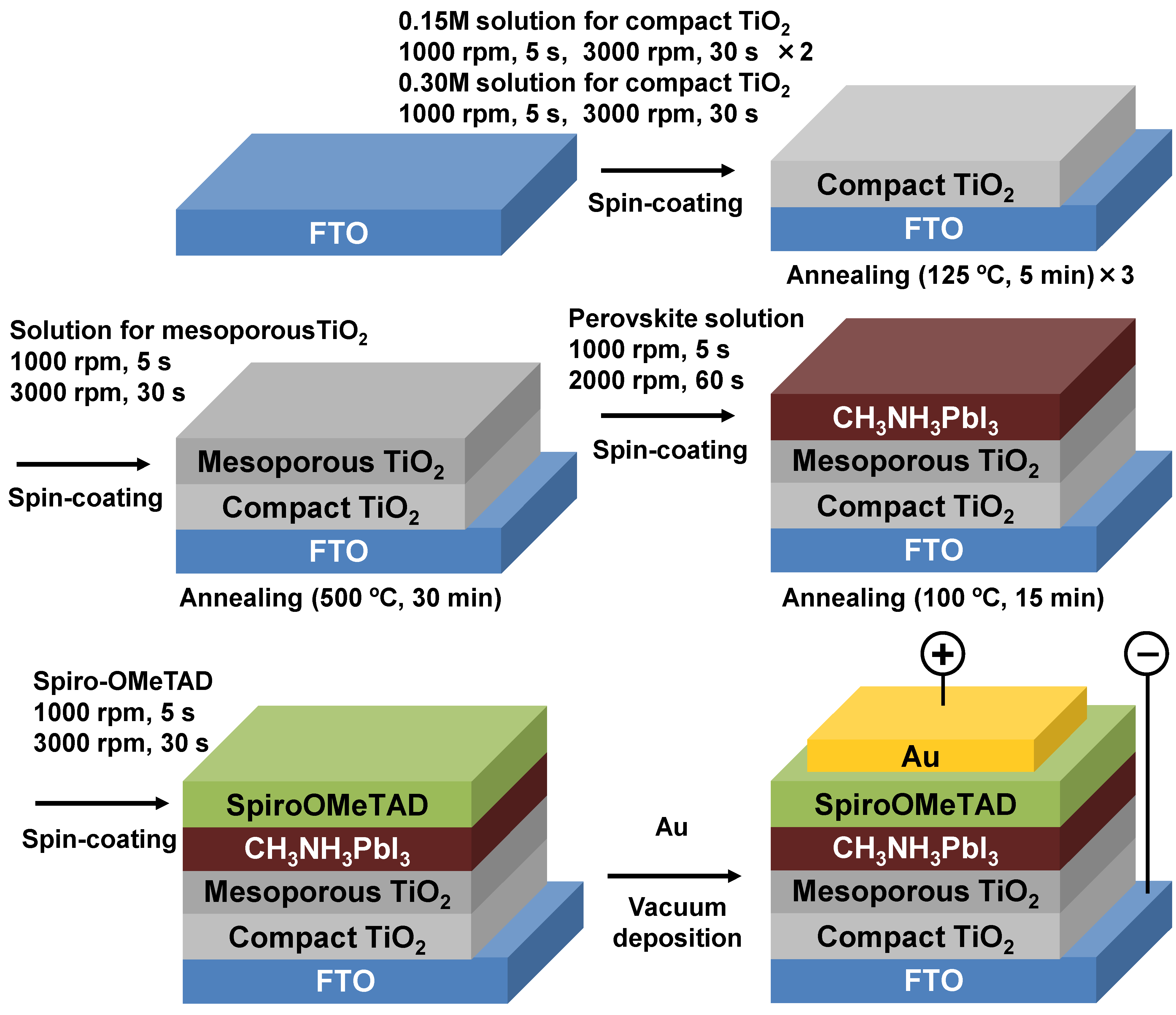
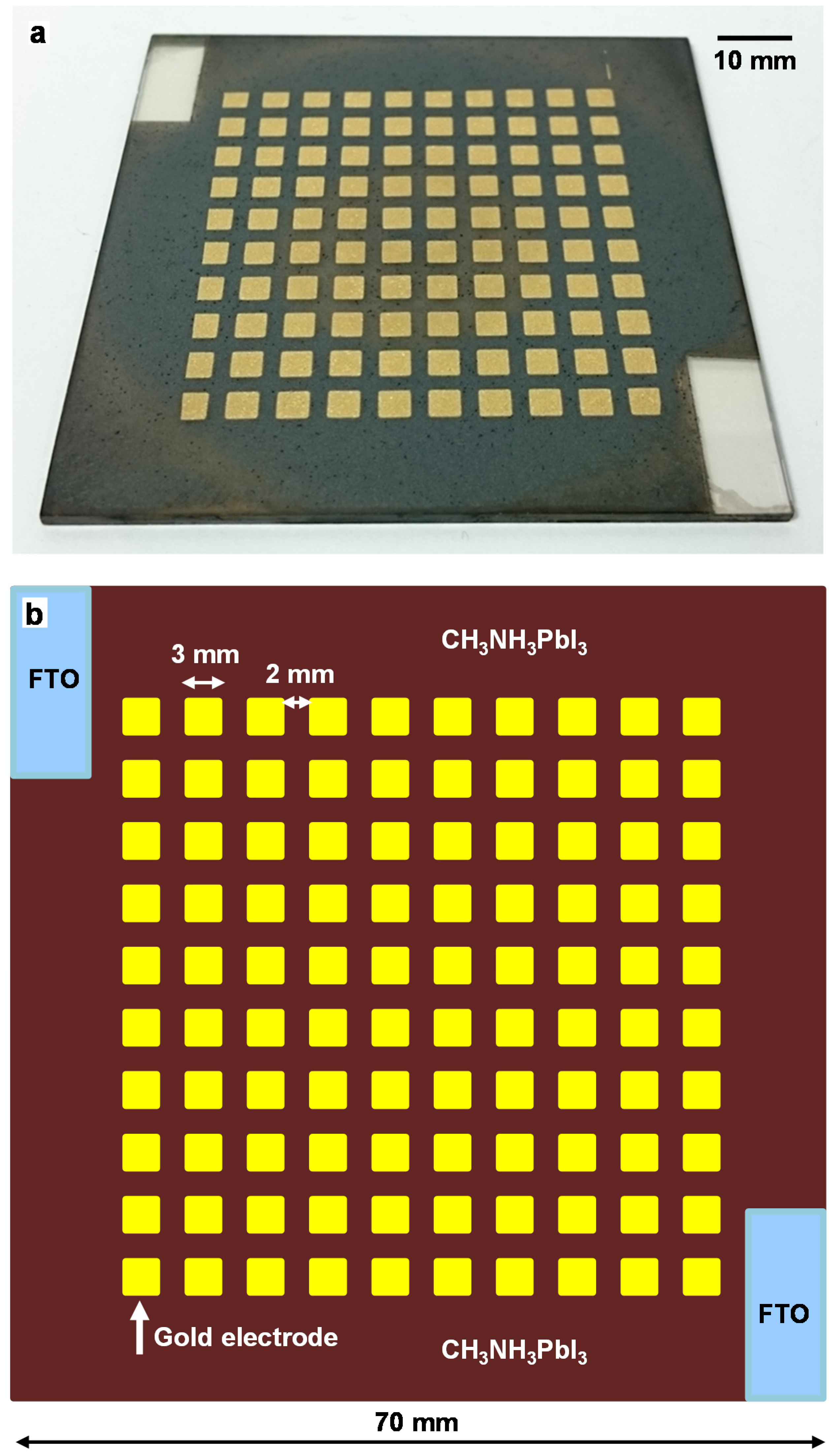
2. Experimental Section

A schematic illustration of the fabrication of the present TiO2/CH3NH3PbI3 photovoltaic cells is shown in Figure 1. Except for the mesoporous TiO2 layer [16], the details of the fabrication process are described in previously reported work [8,17,18]. The cell performance depends on the TiO2 layers and perovskite layers to some extent [19,20,21]. The photovoltaic cells were fabricated by the following process. F-doped tin oxide (FTO) substrates were cleaned in an ultrasonic bath with acetone and methanol and dried with nitrogen gas. The 0.15 M and 0.30 M TiOx precursor solutions were prepared from titanium diisopropoxide bis(acetylacetonate) (Sigma Aldrich, 0.055 mL and 0.11 mL) with 1-butanol (1 mL). First, the 0.15 M TiOx precursor solution was spin-coated on the FTO substrate at 3000 rpm for 30 s and annealed at 125 °C for 5 min. Then, the 0.30 M TiOx precursor solution was spin-coated on the first TiOx layer at 3000 rpm for 30 s and annealed at 125 °C for 5 min. This 0.30 M solution process was performed two times, after which the FTO substrate was sintered at 500 °C for 30 min to form a compact TiO2 layer. For the mesoporous TiO2 layer, a TiO2 paste was prepared with TiO2 powder (Aerosil P-25, 100 mg) and polyethylene glycol (Nacalai Tesque, PEG #20000, 10 mg) in ultrapure water (0.5 mL). The solution was mixed with acetylacetone (Wako Pure Chemical Industries, 10.0 μL) and Triton X-100 (Sigma Aldrich, 5 μL) for 30 min and was left for 12 h to suppress the formation of bubbles in the solution. The obtained TiO2 paste was coated on the substrate by spin-coating at 5000 rpm for 30 s. The cells were annealed at 120 °C for 5 min and at 500 °C for 30 min. CH3NH3I was synthesized by reacting 23.2 mL of methylamine (CH3NH2, Tokyo Chemical Industry) and 25.0 mL of hydroiodic acid at 0 °C for 2 h with stirring. The precipitate was collected by removing the solvents at 50 °C for 1 h. The obtained product was re-dissolved and stirred in diethyl ether for 30 min to remove any impurities and dried using a rotary evaporator at 60 °C for 3 h. The obtained CH3NH3I was finally dried in a vacuum. To prepare pigment with a perovskite structure, a solution of CH3NH3I (98.8 mg) and PbI2 (Sigma Aldrich, 289.3 mg) at a mole ratio of 1:1 inγ-butyrolactone (Nacalai Tesque, 0.5 mL) was mixed at 60 °C. The CH3NH3PbI3 solution was then introduced into the TiO2 mesopores using a spin-coating method and annealed at 100 °C for 15 min. Next, the hole-transport layer was prepared by spin-coating. A solution of spiro-OMeTAD (Wako Pure Chemical Industries, 36.1 mg) in chlorobenzene (Wako Pure Chemical Industries, 0.5 mL) was mixed with a solution of lithium bis(trifluoromethylsulfonyl) imide (Li-TFSI, Tokyo Chemical Industry, 260 mg) in acetonitrile (Nacalai Tesque, 0.5 mL) for 12 h. The former solution and 4-tert-butylpyridine (Aldrich, 14.4 μL) were mixed with the Li-TFSI solution (8.8 μL) for 30 min at 70 °C. All procedures were carried out in air. Finally, gold (Au) metal contacts were evaporated onto the sample as top electrodes. The layered structure of the present photovoltaic cells was denoted as FTO/TiO2/CH3NH3PbI3/spiro-OMeTAD/Au, as shown in the schematic illustration of Figure 1.
Figure 1. Schematic illustration of the fabrication of photovoltaic cells using CH3NH3PbI3 and TiO2.
Coatings 05 00646 g001
The J-V characteristics of the photovoltaic cells were measured (Hokuto Denko, HSV-110) under illumination at 100 mW cm−2 using an AM 1.5 solar simulator (San-ei Electric, XES-301S), and the characteristics depend on the measurement methods [22]. The scan rate and sampling interval were 0.01 V s−1 and 0.1 s, respectively, and a forward scan was used in recording the J-V curves. The solar cells were illuminated through the side of the FTO substrate, and the illuminated area was 0.090 cm2 for each Au electrode. A photograph of a perovskite solar cell measuring 70 mm × 70 mm and a schematic illustration of the arrangement of Au electrodes on the substrate are shown in Figure 2a,b, respectively. The IPCE of the cells was also investigated (Enli Technology, QE-R).
Figure 2. (a) Photograph of perovskite solar cell measuring 70 mm × 70 mm; (b) Schematic illustration of arrangement of Au electrodes on the substrate.
Coatings 05 00646 g002

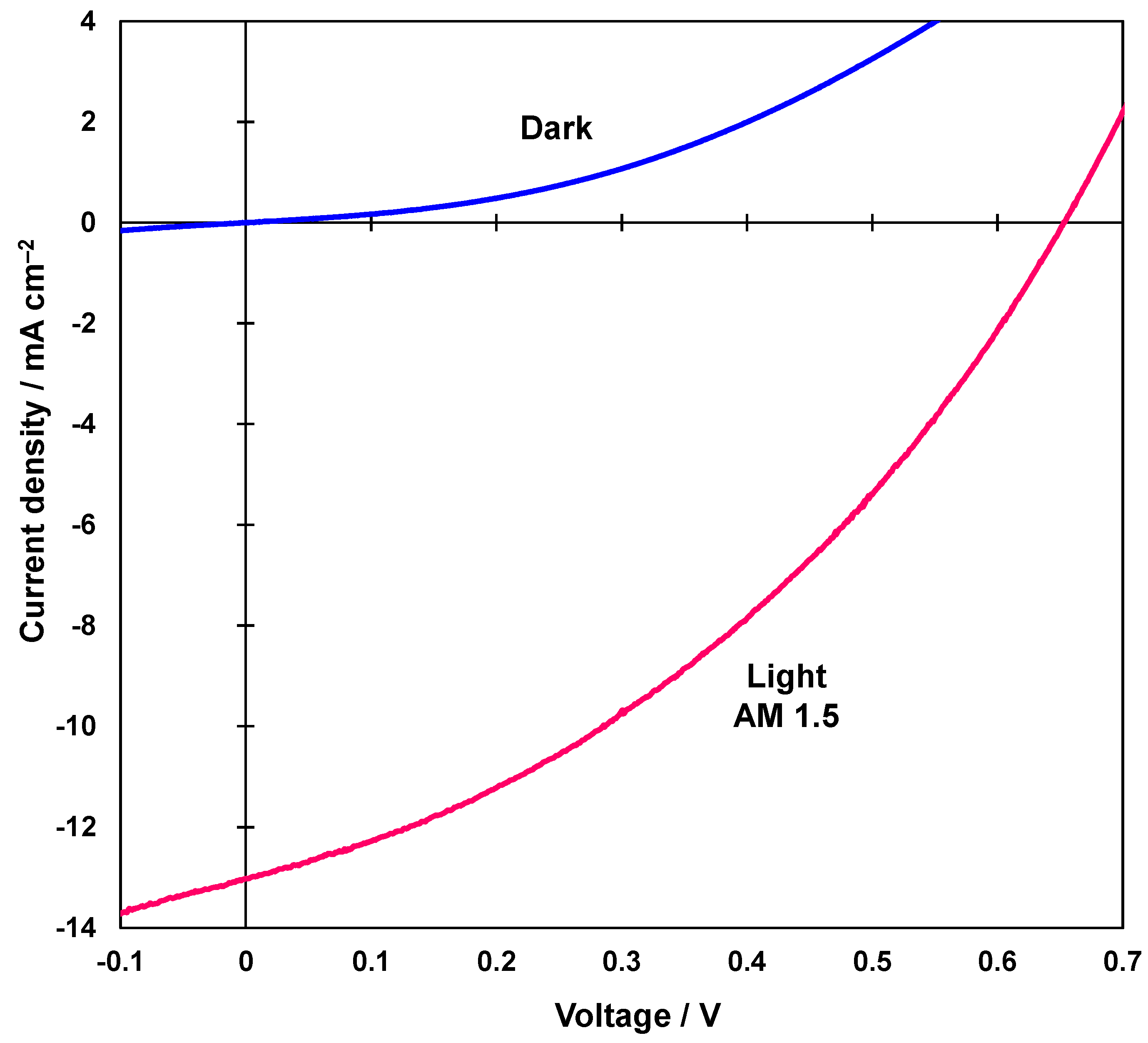
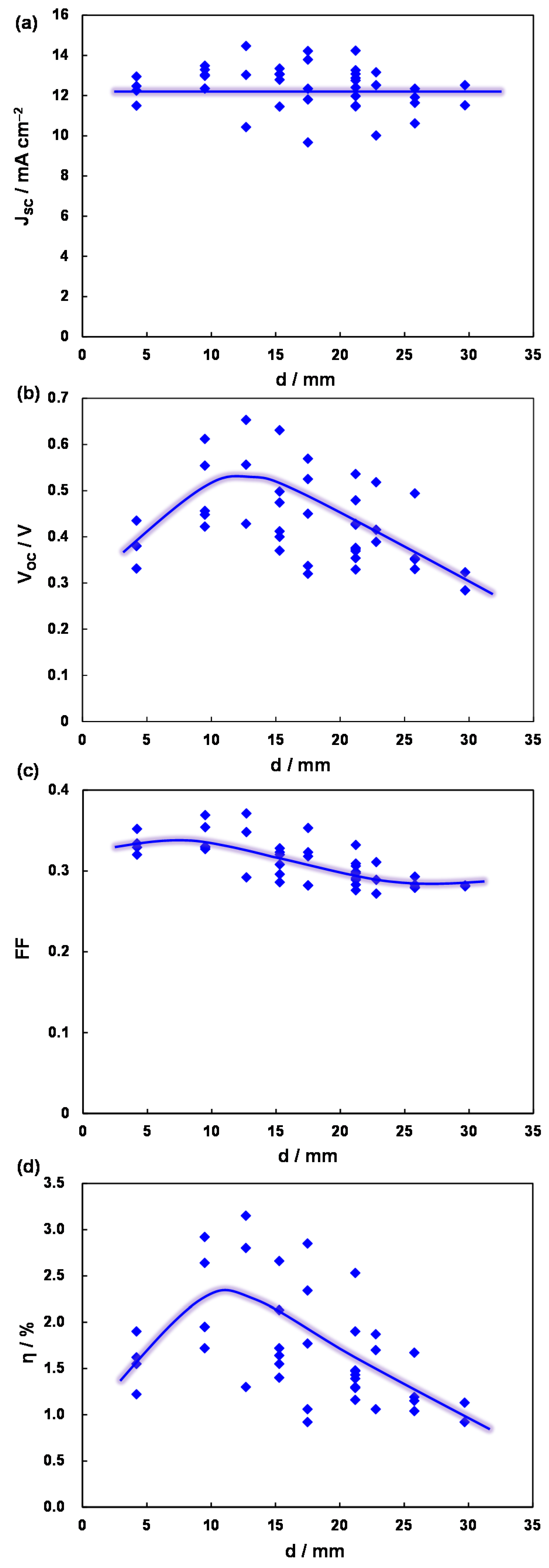
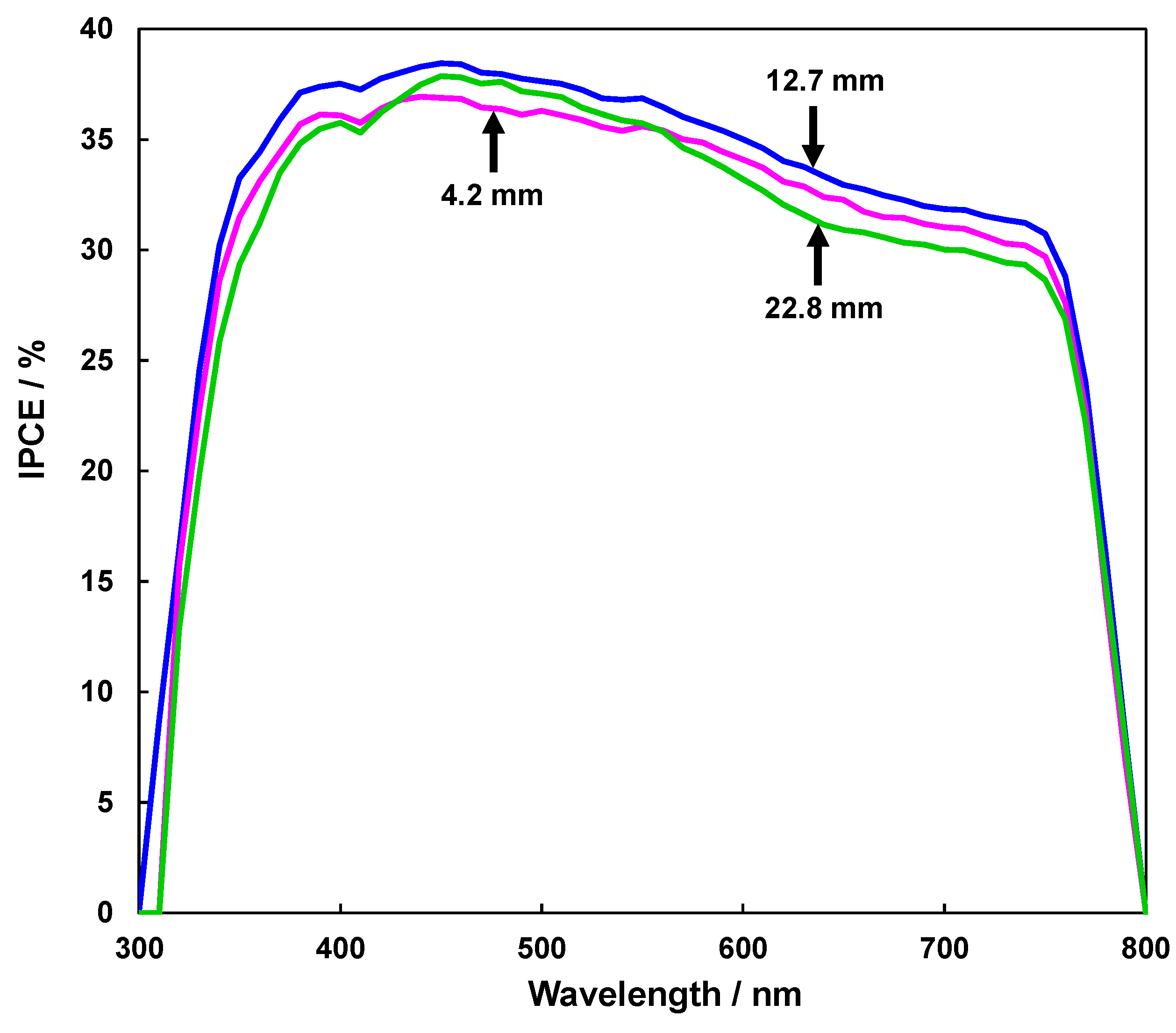
3. Results and Discussion

The J-V characteristics of the TiO2/CH3NH3PbI3/spiro-OMeTAD photovoltaic cells both in the dark and under illumination are shown in Figure 3. No current was observed in the dark, while photocurrent over 10 mA cm−2 was observed under illumination.
Figure 3. Measured J-V characteristics of TiO2/CH3NH3PbI3 photovoltaic cell in the dark and under illumination.
Coatings 05 00646 g003
The measured short-circuit current density, open-circuit voltage, fill factor and photoconversion efficiency of the present TiO2/CH3NH3PbI3 cell as a function of the distance from the center of the cell are shown in Figure 4a–d, respectively. The averaged and top photovoltaic parameters of TiO2/CH3NH3PbI3 cells as a function of the distance (d) from the center of the cell are summarized in Table 1. The highest efficiency was obtained for the electrode at 12.7 mm from the cell center, which provided a photoconversion efficiency (η) of 3.15%, a short-circuit current density (JSC) of 13.0 mA cm−2, an open-circuit voltage (VOC) of 0.653 V and a fill factor (FF) of 0.371.
As a result of a long exciton diffusion length [23], the JSC values were almost constant (~12 mA cm−2) for all electrodes on the cell, as observed in Figure 4a. Although the FF value slightly decreased as d increased, the deviation was not large, as observed in Figure 4c. In contrast, the value of VOC was fairly dependent on d, as observed in Figure 4b and Table 1, which resulted in decreased efficiency, as shown in Figure 4d. The dependency of VOC on the d values might be related to the thickness of CH3NH3PbI3 prepared on the large substrate by spin-coating. The low FF and VOC values would also be related with the coverage ratio of CH3NH3PbI3 at the TiO2/CH3NH3PbI3 interface, and the application of further multiple spin-coating of CH3NH3PbI3 layers on the mesoporous TiO2 layer would improve the coverage of CH3NH3PbI3 on the TiO2, which would lead to the increase of the efficiency of the cells [15].
Figure 4. Measured (a) short-circuit current density; (b) open-circuit voltage; (c) fill factor and (d) conversion efficiency of TiO2/CH3NH3PbI3 cell as a function of the distance from the center of the cell.
Coatings 05 00646 g004
Table 1. Measured photovoltaic parameters (average and top) of TiO2/CH3NH3PbI3 cells as a function of the distance (d) from the center of the cell.
d (mm)JSC (mA cm−2)VOC (V)FFη (%)
4.212.24 (12.94)0.382 (0.435)0.334 (0.352)1.55 (1.90)
9.512.97 (13.47)0.498 (0.612)0.342 (0.369)2.24 (2.92)
12.712.63 (14.46)0.546 (0.653)0.337 (0.371)2.42 (3.15)
15.312.79 (13.33)0.464 (0.631)0.310 (0.323)1.85 (2.66)
17.512.33 (14.21)0.450 (0.569)0.318 (0.353)1.79 (2.85)
21.212.61 (14.23)0.408 (0.536)0.298 (0.332)1.55 (2.53)
22.811.89 (13.15)0.441 (0.518)0.291 (0.311)1.54 (1.87)
25.812.33 (11.62)0.382 (0.494)0.284 (0.293)1.26 (1.67)
29.712.01 (12.51)0.304 (0.323)0.281 (0.282)1.03 (1.13)
Figure 5 shows the IPCE spectra of electrodes at 4.2, 12.7 and 22.8 mm from the cell center. All of the spectra show similar changes with wavelength, which agree with the JSC results shown in Figure 4a. The measurement region was in the range of 300–800 nm, and the perovskite CH3NH3PbI3 structure showed photoconversion within the whole range, which almost agrees with the reported energy gaps of 1.51 eV [24] and 1.61 eV [25] (corresponding to 821 and 770 nm, respectively) for the CH3NH3PbI3 phase. This indicates that excitons and/or free charges were effectively generated in the perovskite layers upon illumination by light of 300–800 nm in wavelength. Previous studies reported experimental evidence for photogenerated free carriers in CH3NH3PbI3 [26], which would enhance carrier transport in the present device. Control of the energy levels of the conduction band and valence band is important for carrier transport in the cell.
Figure 5. Incident photon to current conversion efficiency spectra of the TiO2/CH3NH3PbI3 cell.
Coatings 05 00646 g005
The efficiencies obtained for the present cells are lower than the previously reported values. It seems to be difficult to control the uniformity of the layer thickness and interfacial structure using spin-coating techniques. In the present work, the samples were prepared in air, which may have also resulted in a reduction in the efficiency of the present cells, and perovskite crystals with higher quality and a smooth surface should be prepared in future works.

4. Conclusions

In summary, TiO2/CH3NH3PbI3-based photovoltaic devices with a substrate size of 70 mm were fabricated by a spin-coating method using a mixed solution. The photovoltaic properties of the cells and the size effect were investigated by JV characteristic and IPCE measurements, and the dependence of their photoconversion efficiency on the distance from the center of the cell was investigated. Almost constant values of short-circuit current density were obtained over a large area, owing to the long exciton diffusion length of the CH3NH3PbI3 phase. The open-circuit voltage was fairly dependent on the distance from the center of the cell, which resulted in a change in conversion efficiency. Smoothing and optimizing the layer thickness and structure would be important for improving the device’s performance.

Acknowledgments

This work was partly supported by the Satellite Cluster Program of the Japan Science and Technology Agency and a Grant-in-Aid for Scientific Research (C) 25420760. The authors would like to acknowledge Tsuyoshi Akiyama and Masahito Zushi for useful advice and support.

Author Contributions

Takeo Oku wrote the manuscript and summarized the project. Taisuke Matsumoto fabricated and characterized the solar cells, and summarized the results. Atsushi Suzuki and Kohei Suzuki supported the project.

Conflict of Interest

The authors declare no conflict of interest.

References

  1. Kojima, A.; Teshima, K.; Shirai, Y.; Miyasaka, T. Organometal halide perovskites as visible-light sensitizers for photovoltaic cells. J. Am. Chem. Soc. 2009, 131, 6050–6051. [Google Scholar] [CrossRef] [PubMed]
  2. Im, J.-H.; Lee, C.-R.; Lee, J.-W.; Park, S.-W.; Park, N.-G. 6.5% efficient perovskite quantum-dot-sensitized solar cell. Nanoscale 2011, 3, 4088–4093. [Google Scholar] [CrossRef] [PubMed]
  3. Kim, H.-S.; Lee, C.-R.; Im, J.-H.; Lee, K.-B.; Moehl, T.; Marchioro, A.; Moon, S.-J.; Yum, J.-H.; Humphry-Baker, R.; Moser, J.E.; et al. Lead iodide perovskite sensitized all-solid-state submicron thin film mesoscopic solar cell with efficiency exceeding 9%. Sci. Rep. 2012, 2. [Google Scholar] [CrossRef] [PubMed]
  4. Grinberg, I.; West, D.V.; Torres, M.; Gou, G.; Stein, D.M.; Wu, L.; Chen, G.; Gallo, E.M.; Akbashev, A.; Davies, P.K.; et al. Perovskite oxides for visible-light-absorbing ferroelectric and photovoltaic materials. Nature 2013, 503, 509–512. [Google Scholar] [CrossRef] [PubMed]
  5. Lee, M.M.; Teuscher, J.; Miyasaka, T.; Murakami, T.N.; Snaith, H.J. Efficient hybrid solar cells based on meso-superstructured organometal halide perovskites. Science 2012, 338, 643–647. [Google Scholar] [CrossRef] [PubMed]
  6. Chung, I.; Lee, B.; He, J.Q.; Chang, R.P.H.; Kanatzidis, M.G. All-solid-state dye-sensitized solar cells with high efficiency. Nature 2012, 485, 486–489. [Google Scholar] [CrossRef] [PubMed]
  7. Stranks, S.D.; Eperon, G.E.; Grancini, G.; Menelaou, C.; Alcocer, M.J.P.; Leijtens, T.; Herz, L.M.; Petrozza, A.; Snaith, H.J. Electron-hole diffusion lengths exceeding 1 micrometer in an organometal trihalide perovskite absorber. Science 2013, 342, 341–344. [Google Scholar] [CrossRef] [PubMed]
  8. Burschka, J.; Pellet, N.; Moon, S.-J.; Humphry-Baker, R.; Gao, P.; Nazeeruddin, M.K.; Grätzel, M. Sequential deposition as a route to high-performance perovskite-sensitized solar cells. Nature 2013, 499, 316–320. [Google Scholar] [CrossRef] [PubMed]
  9. Liu, M.; Johnston, M.B.; Snaith, H.J. Efficient planar heterojunction perovskite solar cells by vapour deposition. Nature 2013, 501, 395–398. [Google Scholar] [CrossRef] [PubMed]
  10. Liu, D.; Kelly, T.L. Perovskite solar cells with a planar heterojunction structure prepared using room-temperature solution processing techniques. Nat. Photonics 2014, 8, 133–138. [Google Scholar] [CrossRef]
  11. Wang, J.T.-W.; Ball, J.M.; Barea, E.M.; Abate, A.; Alexander-Webber, J.A.; Huang, J.; Saliba, M.; Mora-Sero, I.; Bisquert, J.; Snaith, H.J.; et al. Low-temperature processed electron collection layers of graphene/TiO2 nanocomposites in thin film perovskite solar cells. Nano Lett. 2014, 14, 724–730. [Google Scholar] [CrossRef] [PubMed]
  12. Wojciechowski, K.; Saliba, M.; Leijtens, T.; Abate, A.; Snaith, H.J. Sub-150 °C processed meso-superstructured perovskite solar cells with enhanced efficiency. Energy Environ. Sci. 2014, 7, 1142–1147. [Google Scholar] [CrossRef]
  13. Zhou, H.; Chen, Q.; Li, G.; Luo, S.; Song, T.-B.; Duan, H.-S.; Hong, Z.; You, J.; Liu, Y.; Yang, Y. Interface engineering of highly efficient perovskite solar cells. Science 2014, 345, 542–546. [Google Scholar] [CrossRef] [PubMed]
  14. Oku, T.; Takeda, A.; Nagata, A.; Kidowaki, H.; Kumada, K.; Fujimoto, K.; Suzuki, A.; Akiyama, T.; Yamasaki, Y.; Ōsawa, E. Microstructures and photovoltaic properties of C60-based solar cells with copper oxides, CuInS2, phthalocyanines, porphyrin, PVK, nanodiamond, germanium and exciton-diffusion blocking layers. Mater. Technol. 2013, 28, 21–39. [Google Scholar] [CrossRef]
  15. Oku, T.; Hori, S.; Suzuki, A.; Akiyama, T.; Yamasaki, Y. Fabrication and characterization of PCBM:P3HT:silicon phthalocyanine bulk heterojunction solar cells with inverted structures. Jpn. J. Appl. Phys. 2014, 53. [Google Scholar] [CrossRef]
  16. Oku, T.; Kakuta, N.; Kobayashi, K.; Suzuki, A.; Kikuchi, K. Fabrication and characterization of TiO2-based dye-sensitized solar cells. Prog. Nat. Sci. 2011, 21, 122–126. [Google Scholar] [CrossRef]
  17. Zushi, M.; Suzuki, A.; Akiyama, T.; Oku, T. Fabrication and characterization of TiO2/CH3NH3PbI3-based photovoltaic devices. Chem. Lett. 2014, 43, 916–918. [Google Scholar] [CrossRef]
  18. Oku, T.; Zushi, M.; Imanishi, Y.; Suzuki, A.; Suzuki, K. Microstructures and photovoltaic properties of perovskite-type CH3NH3PbI3 compounds. Appl. Phys. Express 2014, 7. [Google Scholar] [CrossRef]
  19. Kanayama, M.; Oku, T.; Suzuki, A.; Yamada, M.; Fukunishi, S.; Kohno, K.; Sakamoto, H. Fabrication and characterization of photovoltaic devices based on perovskite compounds with TiO2 nanoparticles. AIP Conf. Proc. 2015, 1649, 84–88. [Google Scholar]
  20. Suzuki, K.; Suzuki, A.; Zushi, M.; Oku, T. Microstructures and properties of CH3NH3PbI3-xClx hybrid solar cells. AIP Conf. Proc. 2015, 1649, 96–101. [Google Scholar]
  21. Oku, T.; Iwata, T.; Suzuki, A. Effects of niobium addition into TiO2 layers on CH3NH3PbI3-based photovoltaic devices. Chem. Lett. 2015, 44, 1033–1035. [Google Scholar] [CrossRef]
  22. Christians, J.A.; Manser, J.S.; Kamat, P.V. Best practices in perovskite solar cell efficiency measurements. Avoiding the error of making bad cells look good. J. Phys. Chem. Lett., 2015, 6, 852–857. [Google Scholar] [CrossRef] [PubMed]
  23. Dong, Q.; Fang, Y.; Shao, Y.; Mulligan, P.; Qiu, J.; Cao, L.; Huang, J. Electron-hole diffusion lengths > 175 μm in solution-grown CH3NH3PbI3 single crystals. Science 2015, 347, 967–970. [Google Scholar] [CrossRef] [PubMed]
  24. Baikie, T.; Fang, Y.; Kadro, J.M.; Schreyer, M.; Wei, F.; Mhaisalkar, S.G.; Gräetzel, M.; White, T.J. Synthesis and crystal chemistry of the hybrid perovskite (CH3NH3)PbI3 for solid-state sensitised solar cell applications. J. Mater. Chem. A 2013, 1, 5628–5641. [Google Scholar] [CrossRef]
  25. Yamada, Y.; Nakamura, T.; Endo, M.; Wakamiya, A.; Kanemitsu, Y. Near-band-edge optical responses of solution-processed organic–inorganic hybrid perovskite CH3NH3PbI3 on mesoporous TiO2 electrodes. Appl. Phys. Express 2014, 7. [Google Scholar] [CrossRef]
  26. Yamada, Y.; Nakamura, T.; Endo, M.; Wakamiya, A.; Kanemitsu, Y. Photocarrier recombination dynamics in perovskite CH3NH3PbI3 for solar cell applications. J. Am. Chem. Soc. 2014, 136, 11610–11613. [Google Scholar] [CrossRef] [PubMed]

