Review

Electrodeposition of Alloys and Compounds in the Era of Microelectronics and Energy Conversion Technology

Department of Materials Science and Engineering, University of Virginia, Charlottesville, VA 22904, USA
Coatings 2015, 5(2), 195-218; https://doi.org/10.3390/coatings5020195
Submission received: 14 May 2015 / Revised: 6 June 2015 / Accepted: 9 June 2015 / Published: 17 June 2015

Abstract

:
Electrochemical deposition methods are increasingly being applied to advanced technology applications, such as microelectronics and, most recently, to energy conversion. Due to the ever growing need for device miniaturization and enhanced performance, vastly improved control of the growth process is required, which in turn necessitates a better understanding of the fundamental phenomena involved. This overview describes the current status of and latest advances in electrodeposition science and technology. Electrochemical growth phenomena are discussed at the macroscopic and atomistic scale, while particular attention is devoted to alloy and compound formation, as well as surface-limited processes. Throughout, the contribution of Professor Foresti and her group to the understanding of electrochemical interfaces and electrodeposition, is highlighted.

1. Introduction

Electrodeposition is a film growth process that consists in the formation of metallic or semiconducting coatings on conductive substrates, starting from metal ion precursors in a suitable solvent and occurring via a charge transfer process [1,2,3,4]. Since nomenclature is somewhat confusing, the term electrodeposition will be used in this paper to refer to a situation where the electrons reducing the metal ion come from the electrode substrate via an external power supply. The electrons needed for metal ion reduction can alternatively be provided by the oxidation of reducing compounds present in solution; this process is usually called, somewhat imprecisely, electroless or autocatalytic deposition [5]. The term electrochemical deposition is more general and refers mostly to both of the processes described above. The discussion in the following will be limited to electrodeposition from aqueous solvents as the only method widely used industrially.
Among the various film growth deposition methods, electrodeposition exhibits several distinctive and somewhat unique characteristics [6]; in contrast to physical deposition methods, it does not require a vacuum environment, thus leading to a simpler reactor design and construction, to minimal capital investment, and simplification of a prospective process scale-up. In addition, it can be carried out at low temperatures (0–100 °C under atmospheric pressure), and the driving force for film growth, the overpotential, can be controlled very precisely (<1 mV) and quickly (~ns) so as to achieve in principle unequaled control over the growth process. These figures should be compared to those of a typical evaporation method, where the driving force is the supersaturation of the evaporating species, which can be controlled only roughly and indirectly by the rate of evaporation, over a time scale of several seconds to minutes.
Electrodeposition was made possible by the availability of the first voltage generator, the Volta pile, and was invented shortly thereafter, in 1803 by Brugnatelli [7]. The first materials to be deposited were Au and Ag, and consequently the initial applications of this technique were limited to decorative purposes. Only later, in the mid-1800s, new solution chemistries were developed—mainly in the UK—to deposit transition and coinage metals, which became widely used to coat steel parts and machining tools in order to increase hardness, enhance corrosion resistance and improve surface finishing as well as appearance [7]. For more than a century electrodeposition was associated exclusively with heavy industry and large scale applications. Much later, in the 1970s, and in concomitance with the information revolution, electrodeposition of magnetic materials was developed at IBM to enable an unprecedented miniaturization of magnetic recording systems [8], and later extending the capabilities of microfabrication methods [9]. Through this transition from the workshop to the bench top, electrodeposition had to improve its image, theretofore associated with toxic fumes and dirty warehouses, and develop new methods and practices, to become compatible with clean rooms and microelectronic fabrication.
Nowadays, electrodeposition is going through a third revolution, prompted by the need to continuously improve the performance of microelectronic and energy conversion devices [10] and, therefore, requiring better material synthesis methods, capable to achieve accurate control of crystal structure and atomic configurations at the nanoscale and sometimes down to the atomic scale. Examples are too many to be discussed in an exhaustive manner, but they include electrical interconnect layers within semiconductor chips [11], thin film magnetic sensors [12] and magnetic field generators at the nanoscale [13], thermoelectric materials and nanostructures [14], and nanostructures for photovoltaics and energy conversion [15,16,17,18]. In order to enable these advances, the science of electrodeposition must be further developed beyond the current state of the art, to achieve a quantitative description of fundamental phenomena at the atomic scale and to control, as well as predict, functional properties.
This essay will focus on the current state of the knowledge and on recent advances in the electrodeposition of alloys and compounds, highlighting the need for close control of structure and morphology as well as tailoring the functional properties. Alloys are of extreme interest in technological applications due to their ability to extend the range of available properties beyond those of pure metals, and to precisely tune such properties via composition and phase selection. Intermetallic compounds, especially those with anisotropic structure, exhibit a range of properties not achievable with any other materials, specifically in the context of magnetic and mechanical/thermal applications. Semiconductor compounds are studied and used for a variety of optical applications, including photovoltaics, palsmonics, and photoelectrochemistry: the synthesis of these materials and the control of their properties are of particular interest as they are determined to a significant extent by a number of features difficult to control, such as stoichiometry, defect density and doping. The contribution of the group of Prof. Maria Luisa Foresti to the understanding of surface limited electrochemical processes, structure, and properties of photovoltaic materials, among other topics, has been and still is profound and long lasting; it is only appropriate that her outstanding achievements be acknowledged and celebrated in this issue.

2. Electrodeposition at the Macroscopic Scale

Electrodeposition is now well understood from the macroscopic standpoint thanks to the thermodynamic and kinetics framework borrowed from electrochemistry.

2.1. Thermodynamics and Redox Potential

Given a solution chemistry, electrochemical equilibria calculations can be used to determine the concentration of free metal ions Az+ and consequently the redox potential Eeq of the reaction Az+ + ze → Acrystal, which is given by the Nernst equation:
E eq (A) = E A z+ 0 + ( RT / zF ) · ln a A z +
where E A z + 0 is the standard redox potential for A, R = 8.314 J/mol·K is the gas constant, T the absolute temperature, z the number of electrons exchanged, F = 96845 A·s/mol is the Faraday constant, and aAz+, is the activity of the ion Az+ [19].
A metal can be electrodeposited from such solution when the potential applied to the substrate electrode Eappl is more negative than Eeq(A); the driving force for film formation is the deviation from equilibrium, and is called overpotential:
η = EapplEeq(A)
note that metal electrodeposition may occur only when the overvoltage is negative. In contrast, a metal in solution is oxidized (it may dissolve in solution, or form an oxide) if the voltage applied is more positive than Eeq(A).
In most practical electrodeposition processes however, a metal A is reduced from Az+ on a foreign substrate S, and an equilibrium for this system cannot be defined rigorously unless the system is left to spontaneously achieve its own equilibrium. In some instances, this equilibrium could be reached quickly—with highly reactive metal substrates for example; in other cases though, for example metal electrodeposition on Silicon, the approach to equilibrium can be sluggish. In this case an onset or nucleation overpotential can be defined, at which deposition starts to occur [20]; this value can be determined for example by using an electrochemical quartz crystal microbalance. The corresponding potential can be significantly more negative (~200 mV) than the redox potential of A, depending on the atomistic details of the nucleation process, which will be considered in Section 3.
The definition of redox potential in the case of the deposition of alloys or compounds is slightly more complex. Two species A and B are present both in the electrolyte and at the alloy electrode; four conditions of equilibrium can be written, and the number of degrees of freedom is zero. This means that of the four activities involved: aAz+, aBw+ in solution, and aAalloy, aBalloy at the electrode, only three are independent. For a generic alloy composition and a generic metal ion concentration ratio the equilibrium conditions may not be all satisfied, and the alloy composition/ion concentration would change in response via selective dissolution or deposition in order to establish equilibrium. Due to the activities of A and B in the alloy being different from unity, the Nernst equations for the two equilibria Az+ + ze → Aalloy and Bw+ + we → Balloy are modified as follows:
E eq (A) alloy = E A z + 0 + ( RT / zF ) · ln a A z + / a Aalloy
E eq (B) alloy = E B w+ 0 + ( RT / wF ) · ln a B w+ / a Balloy
note that these two equilibrium potentials must be the same.
Solution of the equilibrium condition for the A-B system yields the following equation for the redox potential of an alloy system:
E eq = E 0 + R T F x A ln a A Z + + x B ln a B w + z x A + w x B
where
E 0 = Δ G mix F + z x A E A 0 + w x B E B 0 z x A + w x B
Gmix being the free energy of mixing of the alloy, xA and xB = 1 − xA the molar fraction of the components in the alloy, z and w the oxidation states of A and B, respectively. Similar expressions for an n-component alloy are discussed and reported in Reference [21].
If the binary system A-B forms a stable solid solution, ΔGmix is negative and aAalloy, aBalloy are <1. This results in a positive shift of the redox potential of both A and B. This shift in potential can be significant and may lead to a detectable effect; this process is called underpotential codeposition (UPCD) and can be used to grow alloys with improved compositional control, as will be discussed in Section 4.

2.2. Kinetics and Growth Rate

Metal ion reduction occurs via an electron transfer between the ionic species and the electrode; the relationship between current density and overpotential is given by the Butler-Volmer relation [22]:
j = j0[exp(−αfη) − exp((1 − α)fη)]
where j is the current density, j0 the exchange current density, α is the transfer coefficient, f = F/RT, and η the overpotential. Note that Equation (6) implies that a reduction current is positive when the overpotential is negative. This expression can be corrected for mass transfer effects to take into account that eventually, at high overpotentials the reduction rate will be limited by the rate of arrival of ions at the electrode [22]. Under restricting conditions, various approximations of the Butler-Volmer relation can be used at small overpotentials (linear approximation) or high overpotentials (ǀηǀ > 120 mV), the latter being referred to as the Tafel approximation:
j = j0[exp(−αfη)]
Equations (6) and (7) however are strictly valid for a one-electron transfer and are therefore directly applicable only to the reduction of monovalent free ions such as Ag+. Any other metal ion is reduced through a distinct multi-step mechanism, involving a series of electrochemical (charge transfer), as well as other chemical steps. In this case, the reduction rate at steady state is determined by hypothesizing a definite mechanism and writing the rate equations for each step, assuming all these steps to be at equilibrium. Often, one step (the Rate-Determining Step, RDS) is much slower than the others, and this step alone determines the overall kinetics. Only if an electron transfer is the RDS would the j-η relationship depend exponentially on potential, resulting in a quick approach to the limiting mass transfer conditions. A detailed analysis of multi-electron transfer kinetics for various mechanisms is provided in Reference [23].
In the hypothesis that the only electrochemical reaction occurring at the electrode is metal reduction, and assuming the current density j is given, the rate of growth of a pure metal film is given by:
dm/dt = Mj/zF
where dm/dt is the mass deposited per unit area and time, M the atomic weight and z the oxidation state of the element.
In the case of deposition of a binary alloy A-B, assuming that the partial current for the reduction of each element is known, the growth rate is:
dm/dt = (MAjA/z + MBjB/w)
with MA, MB being the atomic weight of A and B, jA, jB , the partial currents for the reduction of the two components, z and w the respective oxidation states. These equations should be corrected in the case that additional spurious reactions (such as hydrogen evolution) occur. Once the partial currents are known, it is also possible to calculate alloy composition:
xA = nA/(nA + nB) = (jA/z)/(jA/z + jB/w)
where ni represents the number of moles of element i.
The application of thermodynamics, kinetics and electrochemical engineering concepts such as the quantification of mass transport and current distribution enable the correct implementation, optimization and scale-up of electrochemical processes, making electrodeposition technology possible. However, this macroscopic approach cannot take into account or predict microstructure, morphology and properties of the material being grown. This aspect becomes more important as we consider the need for a stricter control of difficult to achieve properties, at the nano- and in some cases down to the atomic scale, that requires sophisticated understanding of the atomic processes responsible for the placement of atoms at determined positions within the solid.

3. Electrodeposition at the Atomic Scale

From the atomic standpoint, electrochemical film growth of metals, alloys, or compounds is a multi-step process including transport of ionic species to the electrode, charge transfer, with transformation of the ions into adsorbed atoms, and atom incorporation in the growing crystal.

3.1. Ion Transport

The first step consists in the transport of the metal ions towards the electrode substrate, via convection, migration or diffusion through various spatial regions: (i) the bulk electrolyte, where fluid convection is possible, (ii) the hydrodynamic layer, where convection processes decay closer to the interface and where the fluid velocity increases approximately linearly with the distance from the electrode and saturates at the Prandtl layer thickness (the region close to the electrode where viscosity effects are dominant), and (iii) the Nernst diffusion layer, where no convection may occur and transport is mainly occurring by diffusion for a supported electrolyte. The diffusion layer in aqueous solutions is about 0.1 to 0.5 mm thick; the hydrodynamic layer thickness is about ten times that. Rigorous control over mass transport is possible by using a rotating disk or rotating cylindrical electrode, for which the induced convection velocity field and the Nernst layer thickness can be rigorously calculated [24]. In parallel with mass transport, calculation of the current density distribution over the electrode surface is essential to predict and control the film thickness distribution, the compositional gradient in alloys, and the uniformity in lithographically patterned structures; these calculations are often performed by finite element methods under one of three approximations: purely ohmic drop in the electrolyte bulk, kinetic overvoltage through the double layer, and diffusion limiting conditions [25].
When the metal ion approaches the double layer set up at the electrode/electrolyte interface due to charge separation, the local electric field increases strongly and reaches values of the order of 107–109 V/m, sufficient to strip the water sheath bound to the metal ion. The double layer thickness L is of the order of the nm and depends on the ionic strength of the electrolyte through the relationship:
1 L = e 2 n i 0 z i 2 ε 0 ε r k B T
where e is the electron charge, ni0 and zi are the number density and the charge of ions i, respectively, and the sum is taken over all ionic species present in the electrolyte. In the denominator, ε0 and εr are the vacuum and the relative permittivity, respectively, kB is the Boltzmann constant, and T the absolute temperature.
The importance of the double layer in electrodeposition cannot be overstated; the large interface field in fact strongly affects adsorption processes and atomic surface mobility [26]. While electrodeposition may be similar in many ways to physical vapor deposition PVD, the presence of the double layer results in phenomena that have no counterpart in PVD and that significantly complicate the understanding of fundamental electrochemical growth phenomena.

3.2. Mechanism of Electron Transfer

Electron transfer reactions between a donor and an acceptor molecule have been described by Marcus and Hush [27,28] for the cases of outer and inner sphere electron transfer utilizing a transition state theory approach, which was also generalized to a quantum mechanical theory. A similar theory has been developed for electron transfer between a molecule and an electrode, using the appropriate electronic density of states. In this theory, the rate of electron transfer depends on the distance between the two reacting species, the electronic structure of the donor and the acceptor, as well as the properties of the surrounding solvent. As discussed by Gileadi [29], however, the binding energy of a metal ion to water molecules, about 5 eV (for a monovalent ion) to 20 eV (for a divalent ion), is too large to allow dissociation of the solvated ion at or close to room temperature, inhibiting the occurrence of electron transfer. This analysis has prompted the hypothesis that charge transfer at the interface in electrodeposition may occur via ion tunneling, not electron tunneling as assumed in the Marcus theory. Recent Density Functional Theory modeling of Ag+ reduction at an electrode has shown that the ion in the double layer region exhibits an energy minimum 2.9 Å away from the electrode, sufficiently close to allow the ion to electronically interact with the electrode; the interaction between the 5 s orbital of Ag+ and the sp band of the Ag electrode is therefore sufficiently strong to enable the fast deposition rate that is experimentally observed [30]. This theory, unfortunately, does not describe clearly the dynamic transition from ion to atom that Gileadi sought to understand. In our opinion, the process should be analyzed in terms of the large electric field at the interface using a quantum description for the progressive delocalization of the electron being exchanged. Such a theory has not been considered yet.

3.3. Kinetics of Film Growth

As mentioned earlier, an atomistic description of electrodeposition is often discussed in analogy with physical vapor deposition. In vacuum growth the driving force for deposition is the partial pressure of the atoms present in the gas phase. In electrodeposition instead, the driving force is the overpotential, i.e., the difference between the applied potential and the equilibrium potential of the depositing species. In vacuum, the conditions of film growth are usually described by a dimensionless parameter D/a4F, where a is the lattice constant of the crystal structure being grown (m), D is the adatom diffusion coefficient (m2/s) and F the deposition flux (natoms/m2s). Conventionally, this parameter is referred to in the literature as D/F, assuming a = 1; typical values of D/F then vary between 104 and 108; thermodynamic growth conditions are observed for D/F → ∞, when the ion flux is low and adatoms have sufficient time to settle at minimum energy locations; in contrast, purely kinetically controlled growth obeys the condition D/F → 0, leading to adatoms frozen in metastable configurations [31]. Commercial electrodeposition process are usually very fast and kinetic growth conditions are most common; deposition close to the thermodynamic limit in contrast can be achieved by using very low metal ion concentrations, thus resulting in small current densities that correspond to the diffusion limiting current. The latter conditions are used for fundamental studies, in particular STM growth experiments; see, for example, Reference [32].

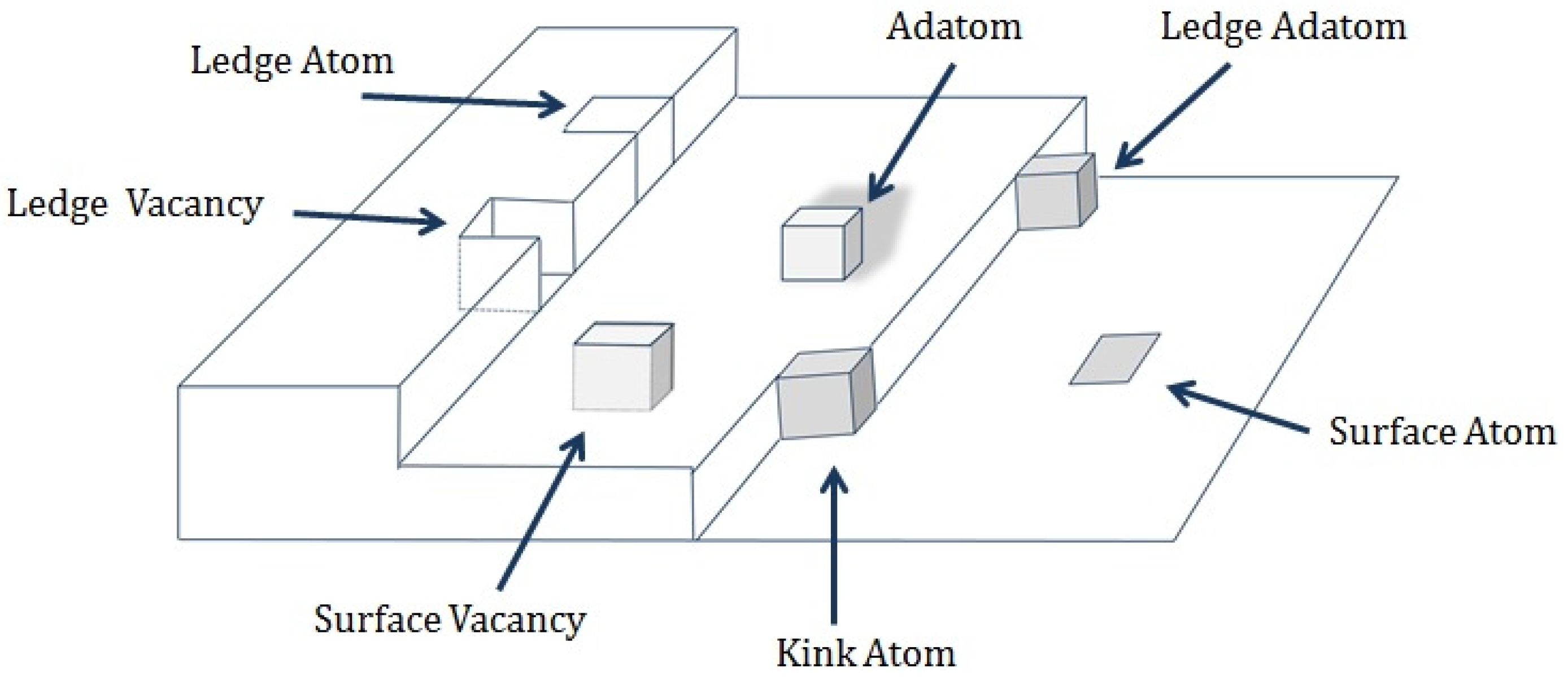
3.4. Growth and Film Morphology

The substrate upon which the film is grown is described by the Terrace-Ledge-Kink (TLK) model (Figure 1), whereby defects on a crystalline surface—mainly steps and kinks—exhibit different numbers of nearest neighbors and, therefore, distinct energetics, with lower number of neighbors implying lower binding energy. At low temperature the surface exhibits a limited concentration of defects and is classified as smooth, meaning that the surface energy as a function of orientation presents sharp minima, leading to a high energetic cost to form a step. Above a critical temperature TR, a surface in vacuum undergoes a roughening transition; typical values of TR are 320–720 K for Cu(11n) surfaces, 450–750 K for Ni surfaces [33]. Above TR the energy to form a step is significantly lowered, resulting in an increase in defect density; note that such surface is not necessarily rough in the usual sense, since height differences may still be small. In electrolytes, the roughening transition may occur close to ambient temperatures, but this transition is strongly affected by the anions present in solution; chloride ions for example restore singular facets in Cu surfaces [34]. On rough surfaces, the density of kinks is reported to be about one every 3rd, 5th atom [35].
Figure 1. Surface sites and defects in the TLK model for a simple cubic (100) surface.
Coatings 05 00195 g001
The kink position (Figure 1) has a particularly important role in defining the equilibrium condition: adding or removing an atom from such position leads to an equivalent configuration, resulting in the same energetics of attachment for the next incoming atom. For this reason, attachment/detachment from the kink site can be used for the definition of equilibrium in electrodeposition [35]; specifically, this occurs when the rate of addition and removal of atoms at kink sites are equal. By applying a negative overvoltage, more metal ions are deposited than removed, and a net flux of metal ions are adsorbed on the substrate while being completely or partially reduced at a terrace, where they may join with other diffusing atoms or diffuse to a kink site; as an alternative, the ion could be reduced at the kink site directly [36]. Analysis of these two processes leads to a different expression for the potential dependence of the growth rate. Direct attachment at kinks results in a B-V type Equation (6), while attachment via diffusion to a kink site results in an apparent transfer coefficient, which is half the value of the former [36]. All these processes are thermally activated; for example, the expression for the diffusivity is:
D = (νda2/4)exp(−Ed/kBT)
νd being an atomic vibration frequency (attempt rate), a the jump distance (roughly the lattice constant), Ed the activation energy for diffusion. If the average diffusion length is sufficiently large adsorbed atoms will encounter other atoms, forming small clusters. Below a critical size these clusters are not stable, due to their additional surface energy. The free energy of formation for a cluster containing N atoms:
ΔG(N) = −Nzeǀηǀ+σ(N)
consists of a bulk term corresponding to the free energy decrease due to the transformation of N ions to a cluster of atoms and a surface term related to the generation of interfaces σ(N). Minimization of the free energy with respect to N results in an expression for the critical free energy ΔGc and the minimum number of atoms Nc needed for the cluster to be stable. In particular, for a 3-D nucleus:
Nc = (8/27)·B·(vm2σ3)/(zeǀηǀ)3
where B depends on the geometrical shape of the nucleus (B = S3/V2, S being the total surface and V the volume of the nucleus) and vm is the atomic volume; and for a 2-D nucleus:
Nc = bsε2/(zeη)2
where b = L2/4S relates the surface area S of the nucleus to its perimeter L, s is the area occupied by an atom on the surface, and ε the line energy [35]. Close to equilibrium the actual shape of the nucleus is determined by minimization of the surface energy; possible nuclei shapes include 3-D (Volmer-Weber type growth) or 2D (Frank-van der Merwe type growth) [37]. With increasing overpotential, the critical nucleus tends to become smaller and more 2-D. The decrease of Nc with increasing overvoltage implies that the nucleus may at a certain point contain few atoms, thereby invalidating the definition of thermodynamic functions, such as chemical potential and surface energy. An atomistic approach to nucleation has been developed [35], which generally resulted in small deviations from the estimates obtained using the continuum approach. It should be noted that the nucleation process dominates only at smooth surfaces; above TR the density of kinks is sufficiently high to directly accommodate incoming adatoms, eliminating any energy barrier for nucleation.
The rate of nucleation is determined by the probability of formation of a critical nucleus and is given by:
J = K·exp(−ΔGc/kBT)
K being a term which takes into account the number of adsorption sites and the rate of attachment of atoms. Assuming first order kinetics for the formation rate of nuclei: dM/dt = −kNM, the number of growing nuclei is given by:
M(t) = M0·[1−exp(−kNt)]
with M0 being the number of nuclei at saturation.
Expression (17) is rarely used, but two limiting cases of instantaneous nucleation
(kNt >> 1): M(t) = M0
and progressive nucleation:
(kNt << 1): M(t) = kNM0t
are often used to derive growth rate laws for 2D or 3D films, leading to expressions for the current vs. time in potentiostatic nucleation, that can be used as a diagnostic to determine the growth mode [38,39]. Note that in order to correctly apply the resulting expressions, it should be insured that no spurious reactions such as hydrogen evolution may occur during metal growth.
Rate equations for film growth yield the number density of adatoms as well as number and size of nuclei as a function of time [37]. These equations can be derived rigorously only for low coverage (typically <0.2 monolayers); at higher coverages, strong interactions among nuclei occur and the probability for secondary nucleation on top of existing nuclei increases. Correlations among nuclei cannot be determined exactly, but general features of growth resulting from interactions can be predicted, including the formation of exclusion zones around the nucleus and the coalescence around a nucleation site during growth under diffusion control. Smooth growth can be achieved if the time necessary for completion of a monolayer via step flow is significantly shorter than the time needed to form a new nucleus. Deposition at low overpotential results in a low nucleation rate, favoring the formation of monocrystalline clusters. Such a growth mode is favored by using defect-free (mainly dislocations) surfaces. The Sofia school has developed a method of electrochemical growth in capillaries to reliably obtain such surfaces; the growth experiments performed with this method are among the most ingenious in this field, so much so that they were able to detect the rate of propagation of steps and the nucleation rate exclusively by current vs. time measurements [40].
On rough surfaces, nucleation preferentially starts at surface defects; steps along crystallographic directions exhibit a low density of kinks, while steps starting at screw dislocations present a high density of kinks. Once nucleation starts, growth occurs through step flow, on various terraces at the same time. The geometrical features of the growing surface depend then on the relative rate of lateral growth vs. growth on top of the terrace.
With increasing overpotential the probability of nucleation increases; in particular, nucleation on top of existing nuclei leads to increasing roughness, due mainly to the presence of an energy barrier (Schwöbel barrier) [41] hindering the downward jump of the atoms located on top. In addition, the appearance of other types of defects is more likely; the most common is twinning, which occurs most easily in face centered cubic (FCC) crystals due to their low twin energy. Formation of twins occurs via nucleation on twin planes ({111} for FCC) and is often the first step towards a transition to a polycrystalline film. Hexagonal structures instead tend to grow along the c axis, which differs from the most probable twin orientations, resulting in twin planes occurring along distinct directions. Twinning energy depends on the crystal structure and on the metal under study, leading to distinct nucleation energetics and morphology evolution for different metal and alloys. Once the film becomes polycrystalline, distinct facets grow at a rate dependent on surface atomic density, with the highest density corresponding to the slowest growth rate. An increase in overpotential further increases probability of defect formation, leading to a characteristic evolution of the preferential orientation with applied voltage.
Twin boundaries and steps at the growing interface are preferential sites for nucleation of new grains. Competitive growth of distinct grains may lead to the formation of a columnar morphology which, if oriented at a small angle with respect to the film normal, result in a columnar structure with high aspect ratio. These columns are usually separated by grain boundaries with lower density, characterized also by a higher density of defects and higher concentration of impurities. Twinning in particular may result either in the formation of faceted growth with apparent growth direction along the twin, or a hemi- or spheroidal growth due to the radial growth from a common nucleus. Large grains are eventually transformed in poly-twinned crystallites, often exhibiting an outward growth and possibly faceting [42].
In-plane growth of islands may lead to compact shapes or fractal-like aggregates; this depends on the adatom surface mobility, with high surface mobility leading to smoother islands due to the increased capability to sample available growth sites. In many cases the observed shapes do not follow the predictions of the diffusion limited aggregation (DLA) model [43,44]; for certain systems in fact no fractal growth is observed, and the width of growth branches is larger than one atom as predicted by DLA. Compact shapes can be obtained only if an adatom is capable to pass through island corners.
Metal islands are usually immobile in electrodeposition, while under vacuum conditions can move only at high T, when diffusion is enhanced and islands may move and ripen. The onset temperature for island ripening is often close to that of the fractal-to-compact island shape transition.
At high overpotential, under high growth rate conditions, the Nernst diffusion layer is depleted in the metal ion, generating a concentration gradient between the bulk electrolyte and the electrolyte/substrate interface, which results in a diffusion current. In presence of any irregularity or protuberance at the electrode, at this location the concentration gradient will be larger, resulting in faster growth at peak than at valleys. Under the linear approximation, the growth at peaks would increase exponentially with time. There are however various effects that counteract this instability. The presence of an overvoltage drop at the electrode due to electrode kinetics implies that in order to accelerate the growth rate the overpotential has to increase, and this can be achieved only by increasing the metal ion concentration at the tip, which decreases the diffusion gradient and the growth rate [45]. Surface energy further acts to stabilize a smooth surface; at high curvature regions in fact the electrochemical potential is increased by the Gibbs-Thompson effect and atoms at these locations tend to diffuse to valleys, decreasing the rate of roughening.
Models of roughening predict that the morphological instability may be facilitated by increasing ion concentration, concentration gradients, presence of excess supporting electrolyte, and decreasing cation concentration at the cathode surface. In particular, a linear stability analysis of morphology evolution finds that concentration gradient is the main parameter controlling morphology, and that surface roughening occurs at progressively shorter wavelengths as the deposition rate is increased, further destabilizing the surface [46].
Possible methods to control the morphology of growing films can be deduced from the fundamental knowledge of growth phenomena. Some examples will be provided in the following. 2-D, compact growth can be enhanced by (i) a decrease of the Schwöbel barrier to increase the probability of the downward jump; (ii) faster corner crossing by adatoms, and (iii) faster surface diffusion to facilitate step flow growth. Hindering edge diffusion and increasing island density would also improve film smoothness, while a low concentration of impurities in the growing film will help to enhance the surface mobility of atoms on top, also accelerating the downward jump. Adding metal surfactants that are highly mobile and immiscible in the film favors 2D growth [47]. The growth mode can also be affected by the substrate; for example, the difference in lattice constant between film and substrate may result in a smooth to 3-D (Stranski-Krastanov) growth transition if the lattice mismatch is small, while it would lead directly to 3-D (Volmer-Weber) growth with a larger mismatch. Additives in the electrolyte may also strongly affect morphology through a variety of phenomena: (i) if the additive is adsorbed strongly to the substrate the nucleation overpotential is increased, resulting in a higher nucleation rate and smaller grains; (ii) selective adsorption at distinct types of defects may alter the ratio of the growth rates along the lateral and vertical directions, possibly leading to alternative geometrical shapes of the film surface features; and (iii) organic surfactants may not inhibit growth at possible growth sites if they are too bulky. While most additives tend to inhibit growth, anions in the electrolyte upon adsorption tend to electronically bridge the metal ion to the substrate, thus accelerating the charge transfer; metal deposition in this case occurs in parallel with the adsorption of the anion, mostly with Br- or Cl-. The growth is now limited at fewer nucleation sites. A judicious combination of inhibitors and accelerators is at the basis of the superfilling technology that has been so successful in providing high quality Cu interconnects within semiconductor chips [48].

4. Overview and Taxonomy of Alloy Deposition Processes

The simplest model for alloy electrodeposition assumes that the two depositing species A and B do not interact during the co-reduction process [49]; if so the total deposition current would be jtot = jA + jB or, in the case that hydrogen reduction (HER) may occur in parallel in the potential range of interest, the equation above becomes:
jtot = jA + jB + jHER
Knowing for each metal reduction reaction (i) the redox potential or the onset potential and (ii) the current density vs. voltage relationship, it is then possible to sketch the theoretical partial current for each component as a function of applied potential and calculate the alloy composition vs. potential.
The current density vs. applied voltage characteristics for metal deposition in the Tafel approximation depends essentially on three parameters, as summarized by Equation (7): the redox potential E, the exchange current j0 and the Tafel slope b; knowledge of these quantities enables sketching of the j-V curves for the single metals and by summation for alloy deposition, allowing calculation of the alloy composition as a function of potential via Equation (10). Consider, for example, Figure 2: Under the approximation of current superposition, knowing the partial currents it is possible to determine the total current (a) (in this case jHER is neglected) and, therefore, the composition as a function of potential (b).
Figure 2. (a) Construction of the jTOT vs. applied voltage characteristics under the assumption of current superposition; (b) The corresponding calculation of alloy composition vs. applied voltage.
Coatings 05 00195 g002
A rich variety of distinct behaviors can actually be seen in practice by varying the three parameters mentioned above and the metal ions concentration; some of those are discussed in detail in Reference [49]. Landolt in particular discusses the fact that the landmark classification of alloy plating systems developed by Brenner [50], including normal, anomalous and induced codeposition, can in part be accounted for by the various features of the partial currents; we add however that some important effects are not.
Unfortunately (or fortunately, for those who are interested in complex processes), the hypothesis of superposition of the partial currents is rarely, if ever, observed in practice. This is due to the various types of interactions occurring between the ionic species being reduced, which may take place at distinct stages of the reduction process.

4.1. Interactions in the Bulk Electrolyte

First, we must consider that the addition of a second metal ion species to an electrolyte affects electrochemical and complexation equilibria in the bulk of the electrolyte, generally resulting in a variation of the exchange currents and diffusion limiting currents for both metals. An example is reported in the Figure 3 below for Co and Co-Ni complexation by citrate before and after the addition of Ni.
Figure 3. Calculated concentration of free Co2+ and free Ni2+ before and after the addition of the Ni ions. Dots: concentration of free Co2+ ions in a solution of 0.1 M CoSO4, 0.2 M NaC6H5O7; triangles: concentration of free Co2+ ions and diamonds: concentration of free Ni2+ ions in a solution of 0.1 M CoSO4, 0.1M NiSO4, 0.2 M NaC6H5O7.
Coatings 05 00195 g003

4.2. Interactions in the Solid

The redox potentials are also affected by the presence of the additional metal, as discussed in Section 2 on equilibria at alloy surfaces. Specifically, the redox potential of the less noble metal during alloy deposition is shifted with respect to the redox potential of Me ion on Me substrate due to the free energy of mixing ΔGmix; formation of solid solutions in particular results in a redox potential shift in the positive direction; the phenomenon is referred to as underpotential co-deposition (UPCD). The relationship between the free energy of mixing [51]:
ΔGmix = ΔHmixTΔSmix= (WGAxA + WGBxB)xAxB + RT(xAlnxA + xBlnxB)
the activity of the element in the alloy, and the UPCD shift from Equations (3)–(5) can be used to predict the alloy composition as a function of potential, under the approximation that the deposition process is sufficiently slow to approximate thermodynamic conditions.
The possibility to observe UPCD and to utilize bulk thermodynamic data to predict alloy composition vs. applied potential was validated by investigating the electrodeposition of Au-Cu alloy from non-complexing solutions, showing that the theoretical expression Equation (3), with aalloy derived from Equation (21) is able to reproduce the whole range of composition vs. potential [52]. Earlier works focused on the UPCD of Pt alloys for magnetic and catalytic applications, demonstrating again that alloy composition could be closely controlled [53,54,55]. UPCD of Pt with the transition metals Fe, Co, Ni however resulted in codeposition only under diffusion limiting conditions for Pt, resulting in hydrogen evolution, pH increase at the interface, and oxygen incorporation in the films [54]. This problem was overcome by utilizing a Pt complex to shift the onset of Pt deposition more negative, leading to closer onset potentials for Fe and Pt and mostly avoiding oxygen incorporation [56,57]; the improved purity also resulted in an earlier onset of the phase transformation of FCC Fe-Pt to the high anisotropy tetragonal structure of interest in magnetic recording [58].
The UPCD process is an extremely intriguing phenomenon, in particular for the possibility to probe the alloy structure and their atomic configuration starting from the thermodynamic equilibrium conditions to kinetically dominated growth processes. A most interesting observation for example is the possibility to access metastable configurations in electrodeposited Au-Ni alloys; while bulk Au-Ni tends to phase separate in two elemental structure, electroplated films under UPCD conditions exhibit a two-phase configuration consisting of Au-rich grains and Ni-rich grain boundaries [59].
The binding energy involved in the UPD process is also active during the formation of intermetallic and semiconductor compounds, as well as in ordered structures. The main difference with respect to solid solutions is that the compositional range of stability is limited, resulting in a free energy which increases strongly as soon as the composition departs from the stoichiometric value. This results in the unique opportunity of electrodeposition processes to form high quality semiconductor compounds with precise stoichiometry and tunable properties by deviating from that stoichiometry [60].

4.3. Interactions at the Interface

Interactions between reaction intermediates can also occur at the electrolyte/electrode interface. The two components A and B that are being reduced generally do so through a multi-step mechanism, and some of the resulting intermediates invariably adsorb on the substrate before they are further reduced. These reaction intermediates may therefore compete for adsorption at the electrode, mutually affecting the relative reduction rate and therefore alloy composition. An important example of this effect is the anomalous deposition observed in the formation of mutual alloys of Fe group metals (Fe, Co, and Ni), and in some cases with Zn. In anomalous deposition, the less noble metal is present in large quantities in the deposit, much higher than expected based on the relative metal ion concentration. Understanding of this process has developed over many years; the main reason for the detailed and prolonged investigations of this process is related to the technological importance of Fe-Ni deposition for magnetic recording heads, magnetic shields and sensors [61]. This is probably a main reason why Fe-Ni electrodeposition is today one of the few alloy electrodeposition processes implemented industrially. The first explanation of anomalous codeposition [62] involved the formation of a hydroxide layer at the substrate, inhibiting Ni deposition due to the larger hydrolysis constant of Fe. This phenomenon is currently better understood in terms of a two-step reduction process for both elements, the first step being a one electron process from the divalent metal Me(II) ion (Me = Fe, Ni) to a monovalent complex Me(I) that has been hypothesized to be Me(OH)+ in sulfate solutions and MeCl+ in chloride solutions. Calculation of the potential dependence of adsorption of Me(I) and Fe(I) shows that the Fe(I) adsorbs at much more positive potentials than Ni(I), and in the case of competitive adsorption, the rate of adsorption of Ni(I) is strongly inhibited, resulting in a low Ni fraction in the alloy [63]. Anomalous codeposition occurs only under activation control for both metals, and this phenomenon disappears at high overpotentials, under diffusion limiting conditions. More recently, it has been observed that not only codeposition of Fe inhibits Ni reduction, but also Ni codeposition enhances the Fe reduction rate, meaning that the absolute reduction rate of Fe is increased with respect to that of Fe alone in the presence of Ni2+ in solution. This latter effect has not been fully understood yet but mathematical models have been proposed, where a mixed complex is assumed to form at the surface, providing an additional route for Fe reduction [64,65].
The process of induced codeposition has also been interpreted through this general mechanism. Induced codeposition is a phenomenon whereby Mo and W, two metals that cannot be electrodeposited in elemental form from aqueous solutions, can instead be co-deposited with Fe-group metals. This process has been studied in detail by Landolt’s group, who focused mainly on Mo-Ni [66,67], and later by Gileadi, who focused instead on W-Ni [68,69]. Experiments show that in electrolytes with low Mo (W) concentration Ni is deposited under kinetic control, and Mo (W) is incorporated under diffusion limiting conditions; in electrolytes with high Mo content instead the alloy composition does not change irrespective of electrolyte stirring, leading to the conclusion that both elements are deposited under diffusion limited conditions. In other words, the non-plateable metal deposits at a rate determined by the reduction rate of the Fe-group metal. These observations have been rationalized by assuming the formation in solution of a mixed metal complex that may enable the deposition of the difficult to plate metal. The alloys formed by these process tend to be Ni-rich, with the Mo (W) concentration being up to 50 at%, suggesting that deposition may occur via two parallel paths, Ni deposition from its own complex and Ni-Mo (Ni-W) depositing from the mixed complex. While Landolt has given only a general expression for this complex [66,67], Gileadi assumes that this complex is of the form (Ni)(WO4)(Cit)H2− [69], linking its stoichiometry to the limiting composition (~50:50) that has been achieved. More recently, the observed increase in Re faradaic efficiency (FE) when codeposited with Ni has been interpreted along the same lines, despite the fact that elemental Re can be deposited, even if only at low FE. Specifically, the Re deposition rate is found to be accelerated by an electroless process involving metallic Ni on the substrate, the oxidation of which enables the reduction of ReO− 4 to ReO− 3or Re0. The hypothesis of an induced deposition process via a mixed complex was ruled out due to the fact that compositions with Re > 50 at% could be achieved [70].

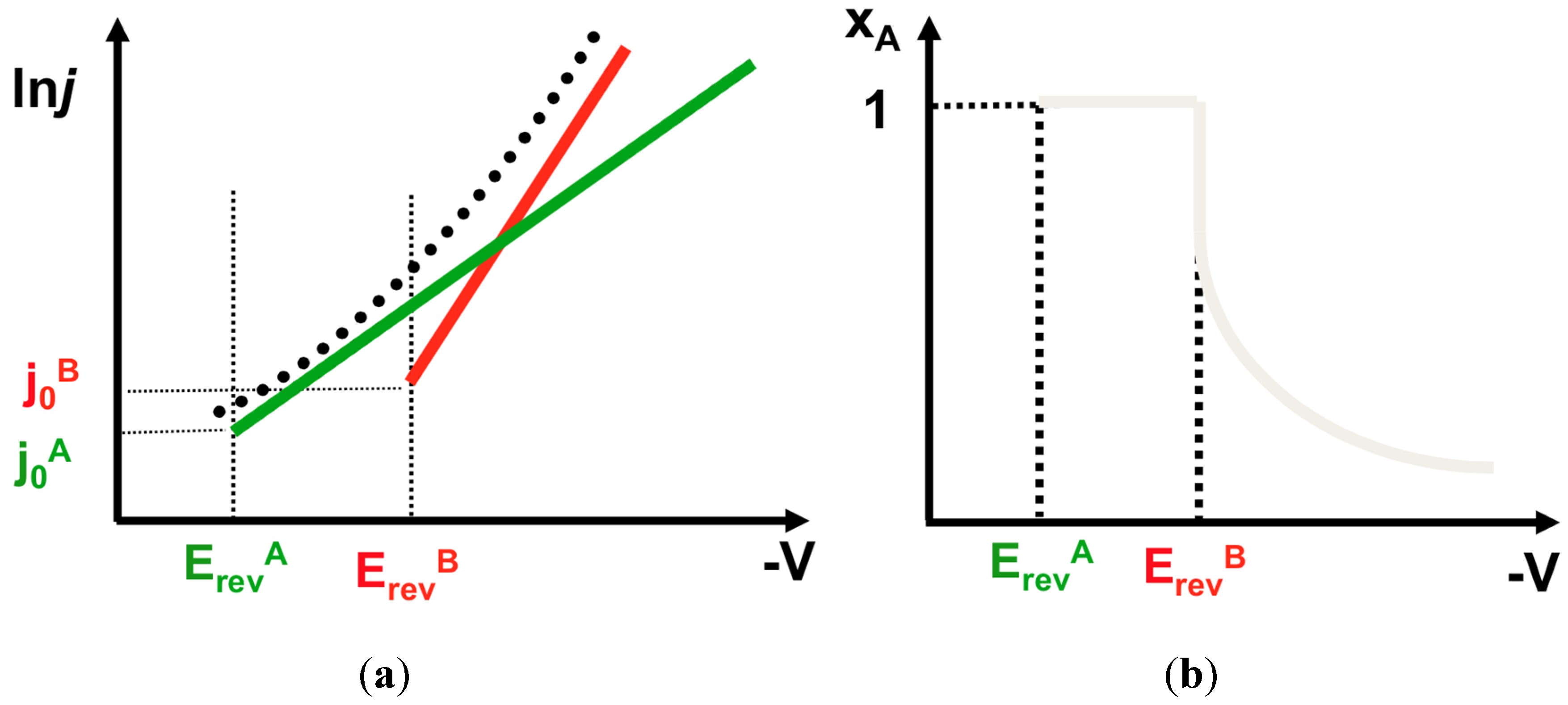
4.4. Peculiarities of Alloy Deposition

The formation of an alloy, or in general a heterogeneous surface results in a position-dependent energy barrier for the surface diffusion of adatoms, which may affect surface mobility and therefore microstructure. Additionally, crystal formation at an alloy surface is affected by various contributions to the overall binding energy of the system, which includes not only the pairwise and cluster atomic interaction among the various components, but also the strain effects originated by the difference in atomic volume among the components. Changes in alloy binding energy result, as seen in Section 2, in a shift of the redox potentials. In addition, atomic configuration at kink sites may affect the probability of attachment and the residence time of an adsorbed atom, in dependence of the identity and position of the surrounding atoms. Relative probabilities for attachment of the two elements at a kink site have been calculated by Plieth, who showed also the possibility to relate these values to alloy composition and to the formation of a solid solution vs. an intermetallic compound [71,72].
Today, due to the refinement of characterization methods and the development in electrochemical analytical techniques, the state of knowledge in alloy electrodeposition is much more advanced than it was at the time of Brenner; however, we are still far from developing a general theory of electrodeposition, capable to control and predict structure and properties of the material as a function of electrolyte chemistry and deposition conditions.

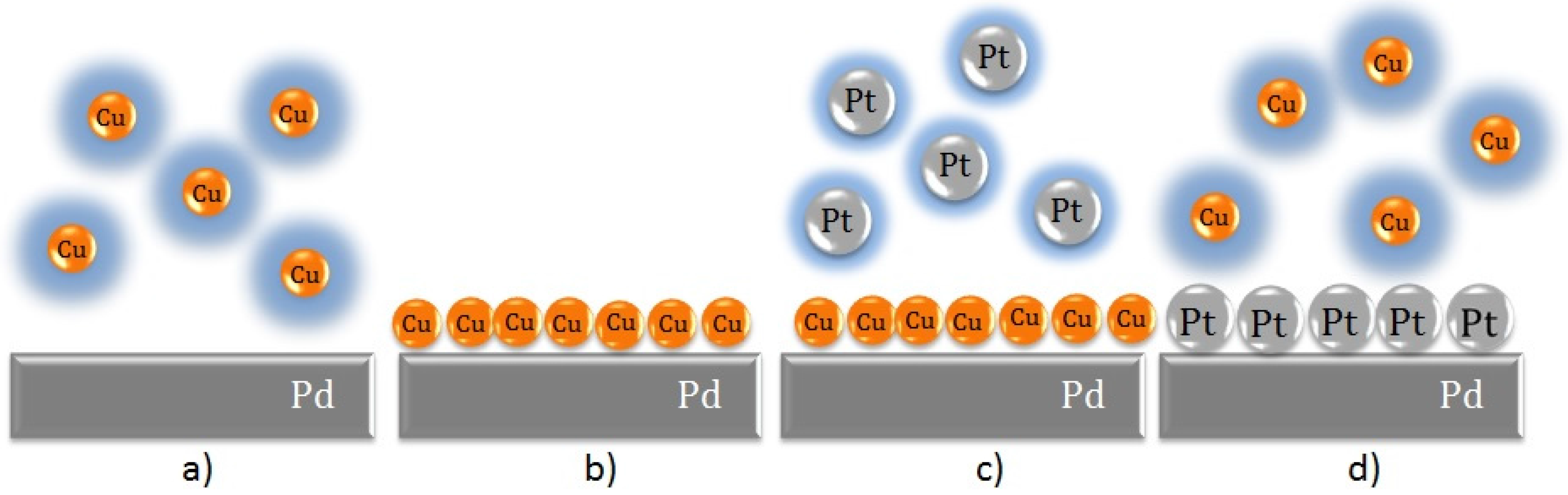
5. Surface-Limited Electrochemical Processes for Materials Synthesis

Underpotential deposition (UPD) is an electrochemical surface process involving the deposition of one (or sometimes two) monoatomic layers of a metal on an electrode surface at an applied potential more positive than its equilibrium potential. UPD exhibits pronounced sensitivity to the atomistic features of the electrode surface, and has been used to estimate true surface area, in particular surface roughness, and for the decoration of selected surface features, for example in corroded samples. UPD, however, has been mainly used as a method for surface modification for the purpose of improving functional properties, such as catalytic activity and selectivity [51]; in particular, UPD phenomena are used extensively to form nanomaterials with controlled structure and atomic configuration, down to the atomic scale.
UPD may occur thanks to the attractive interactions M-S between the depositing metal ion Mz+ and the substrate S being stronger than the pairwise atomic interactions for M-M and S-S. UPD is unique to electrochemical processes; it is in fact possible only due to the low energy of the precursor ions (of the order of kT ~ 0.025 eV), which is of the order of the typical interaction in bulk alloys, typically between 0.01 eV and 0.1 eV. The first comprehensive work on UPD phenomena was carried out by Kolb whom, upon studying a large set of M-S pairs, derived a phenomenological correlation between the underpotential shift ΔEUPD and the work function Φ of M and S [73]:
ΔEUPD = 0.5 V/eV·(ΦS−ΦM)
The functional form of this correlation was later justified by thermodynamic reasoning, setting up a Born-Haber cycle for the transformation of Mz+ to M-S [74].
UPD involves the potential dependent adsorption and partial or complete reduction of Mz+; the details of this process are determined by various features, including the difference in electronegativity of the two elements, the attractive forces M-S, and the repulsive interaction between UPD atoms. In addition, strain developing during the growth process may contribute to the overall energetics of the system.
On ideal single crystal surfaces the UPD process would result in the formation of an epitaxial monoatomic layer of M on top of S, with the structure of the overlayer being determined by the atomic size difference and the detailed atomic interactions. Any single crystal surface at room temperature however presents various defect sites (terraces, ledges, kinks, vacancies, dislocations) that exhibit lower coordination, higher energy, and are therefore preferential sites for the nucleation of the films. This implies that only by using high quality (single crystal) surfaces the UPD process may approach the ideal behavior; in most cases, nucleation and growth of the monolayer would occur preferentially at defect sites and spread from there; additionally, multilayers may be formed due to the substrate inhomogeneity and roughness.
The Surface Limited Replacement Reaction (SLRR) process has been developed by Brankovic et al. as a modification of the UPD process [75]; this phenomenon consists in the replacement of a UPD layer M on a substrate S by a more noble metal ion, N. The first step of this process consists in the deposition of M at UPD on a suitable substrate, followed by the replacement of M by N at the open circuit potential; the driving force is provided by the difference in redox potential of the two metals. A typical example of this process involves the replacement of a Cu UPD monolayer on Au single crystal by Pt (Figure 4). This process mimics the well known cementation phenomenon, with the only difference that SLRR is limited to the atomic layer level. In some cases, SLRR can be simplified by first performing UPD of the metal M, followed by injection of the metal N in the electrolyte, using a one-pot process [76]. SLRR has also been extended to the use of non-metallic sacrificial monolayers; for example, a UPD hydrogen layer has been used as a sacrificial layer to perform metal replacement [77]. Repetition of this process leads ideally to a homo- or hetero-epitaxial layer of high quality that could be used for particular functional applications.
The metal replacement process must obey the conditions of electroneutrality; as a consequence, if the metal M has a different oxidation state from metal N, the monolayer may not be complete. For example, consider the replacement of UPD Cu by PtCl 6 2 in solution. At first sight, one might think that the Pt4+ reduction may require oxidation of two Cu atoms to Cu2+, leading to the overall reduction of 0.5 ML of Pt. In presence of Cl however, Cu is oxidized to CuCl 2 , i.e., to Cu+, therefore, the coverage by Pt would be only 0.25 mL. In reality, other modes of Pt reduction related to the presence of defects lead to an increased coverage [78].
Figure 4. Schematics of the Surface Limited Redox Reaction process. (a) immersion of Pd substrate in Cu2+ solution; (b) UPD of Cu monolayer on Pd; (c) rinsing and immersion in a Pt4+ solution; (d) the Pt ions are exchanged with Cu atoms to form a Pt submonolayer.
Coatings 05 00195 g004
An original modification of the SLRR method has been developed in Foresti’s group in Florence, and is based on the oxidative UPD of S2- from sulfide solution to sulfur monolayers. Transition metals (TMs), such as Mn, Fe, Co, Ni, tend not to UPD on noble metals, such as Au or Ag, but, as a consequence of the strong bonding interactions in TM sulfides, they can UPD on sulfur monolayers. After formation of the TM-S bilayer, the S layer is removed by reducing it back to S2-, leaving the TM monolayer behind. This method has been named Selective Electrodesorption Based Atomic Layer Deposition (SEBALD) [79]. An additional variant of this process is the use of oxygen monolayers instead of S monolayers; it has been claimed for example that an oxidized Au surface can be used to form a UPD Zn layer; repeating this process a ZnO film made up of Zn/O bilayers can be formed [80].
The first method exploiting UPD processes for the formation of functional films has been pioneered by John Stickney at the University of Georgia, and has been called ElectroChemical Atomic Layer Epitaxy (ECALE) [81]. Important advances towards the development of this process have also been achieved by the group of Prof. Foresti in Florence. This method ideally enables the formation of compound semiconductors one atomic layer at a time, each layer being deposited under UPD conditions. The successive layers are deposited in a cyclic fashion, using ranges of potentials that are compatible with each other, that is, that do not involve dissolution or oxidation of the monolayers already formed. The ideal process works by approaching thermodynamic equilibrium conditions, that is, by allowing electro-adsorption of the monolayer to continue until completion; this should result in precise epitaxial, layer-by-layer growth. The inescapable defects and the possible sluggish kinetics of some adsorption process however may hinder the formation of ideally layered compounds. Each semiconductor compound system shows a distinct behavior and consequently involves different electrochemical cycles. Some systems could be formed by oxidation-reduction (O-R) cycles, but their number is limited to the few elements that exhibit an oxidative deposition chemistry: S, Se, Te, and few others. It is possible to make compounds by R-R cycles, but if it is possible to deposit A over B it is thermodynamically impossible to deposit B over A, due to the possible dissolution. One can, however, rely on the sluggish dissolution kinetics to avoid dissolution.
In order to achieve monolayers during the single UPD cycles and eventually high quality semiconductors compounds the chemistry, deposition potentials and duration of the monolayer adsorption process must all be optimized. Some studies on the kinetics of UPD and SLRR processes are available [82], but complications related to the presence of defect sites and potential-dependent kinetics require empirical optimization of the process. The structure of surfaces in fact and the kinetics of reduction processes are not ideal, due to the range of available adsorption/reduction sites, surface heterogeneity and therefore the possibility to form inhomogeneous layers. Due to this inhomogeneity, atoms in high energy sites tend to redissolve and reduce at more stable sites; this process is hardly distinguishable from surface diffusion.
In the following an ECALE process for the electrodeposition of CdS from the work of Foresti’s group will be illustrated [83]. Figure 5a reports the cyclic voltammetry data at a Ag(111) single crystal immersed in a pH 9.2 ammonia buffer solution containing 0.5 mM Na2S; oxidative deposition of S is observed around −0.8 VSCE. Figure 5b shows the cyclic voltammetry for Cd reduction from a pH 9.2 ammonia buffer with 0.5 mM CdSO4 at a Ag(111) singe crystal, bare (broken trace) and modified with a S monolayer (continuous trace). The ECALE cycle consists in the oxidation of S from Na2S at −0.75 VSCE, followed by rinsing of the cell, and injection of the Cd solution into the cell while keeping the same potential constant for about 30 s.
In this work, the quality of the layer-by-layer growth process was demonstrated by the possibility to deposit up to 150 deposition cycles, maintaining a linear increase of the stripping charge measured for both Cd oxidation and S reduction, and also by the 1:1 stoichiometry observed by XPS [83].
The power of surface limited electrochemical deposition processes is also demonstrated by the recent trend to use SLRR for the modification of nanoparticles with metallic monolayers. Platinum is the most popular catalyst for fuel cell (FC) electrodes; one of the most important obstacles to the widespread adoption of this technology to transportation applications, beyond the durability, is the high amount of Pt needed to sufficiently accelerate the oxygen reduction reaction (ORR) at FC cathodes. An efficient way to minimize the Pt content with respect to Pt nanoparticles is to perform SLRR of Pt monolayers on nanoparticle substrate modified first with an UPD Cu monolayer. Pt monolayers on Pd nanoparticles have been shown to initially perform much better than standard Pt/C catalysts and to maintain their mass activity for a longer time. The quality of the coatings achieved by these methods is directly demonstrated by HAADF-STEM (High Angle Annular Dark Field–Scanning Transmission Electron Microscopy) images and their reconstruction using the structure model for 1 Pt ML on Pd (top) and 4 Pt MLs on Pd (bottom), which validate the ability to deposit single MLs of Pt (Figure 6) [84].
Figure 5. ECALE cycle for CdS deposition. (a) cyclic voltammetry for an ammonia buffered solution containing Na2S at a Ag(111) single crystal. (b) cyclic voltammetry for an ammonia buffered solution containing CdSO4 at a Ag(111) single crystal (broken trace) and a S-covered Ag(111) (continuous trace). From Reference [83], reproduced with permission of the Electrochemical Society.
Coatings 05 00195 g005
Figure 6. (a,b) HAADF-STEM images of Pt@Pd nanoparticles: (a) 1 ML Pt, (b) 4 ML Pt. (c,d) Intensity profiles from scan lines across images (a) and (b), respectively. (e,f) reconstruction of the atomic structure of (a) and (b) and structure models. Reprinted with permission from Reference [84]. Copyright 2009 American Chemical Society.
Coatings 05 00195 g006

6. Final Remarks

The ongoing miniaturization of devices and the necessity to improve performance or enable new functions in microsystems requires the accurate synthesis of materials with complex structures, including alloys and intermetallic or semiconductor compounds. In extreme cases the required functionality may need nano- to atomic-scale control of the placement of atoms at predetermined locations.
Electrochemical deposition has a considerable potential to successfully overcome this challenge; the possibility to finely control the degree of irreversibility of the growth process via the overpotential, and the ability to exploit interatomic interactions to guide growth due to the low energy of the metal ion precursors represent only two of the many advantages of this technique. In particular, the close control of the driving force enables the formation of quasi-equilibrium structures, useful for example in the formation of ordered phases or intrinsic semiconductor compounds. At the same time, it is possible to tune continuously the degree of metastability of the structure being grown, with the possibility to correspondingly tune properties, via alloy composition and atomic configuration in metals, and through dopant density, impurity concentration and defects in semiconductors.
In addition, a variety of surface-limited processes is also available to potentially grow single metallic monolayers or ordered semiconductor compounds with a precision which is limited only by the quality of the substrate and the level of precision of the synthesis process.
Progress in microelectronics and energy technology hinges heavily on the availability of methods to precisely grow materials with predetermined properties, at a large scale and economically; electrodeposition has a bright future in this context, as it can be easily scaled-up, it enables formation of materials at low temperature, and allows surface processes to be exploited in the synthesis of nanomaterials.

Acknowledgement

This work was partly supported through the awards NSF CMMI 1131571 and NSF DMR 1207351. The author thanks Begum Unveroglu at UVa for preparing Figure 1 and Figure 4.

Conflicts of Interest

The authors declare no conflict of interest.

References

  1. Gamburg, Y.D.; Zangari, G. Theory and Practice of Metal Electrodeposition; Springer: New York, NY, USA, 2011. [Google Scholar]
  2. Dini, J.W. Electrodeposition: The Materials Science of Coatings and Substrates; Noyes Publications: Park Ridge, NJ, USA, 1993. [Google Scholar]
  3. Schlesinger, M.; Paunovic, M. Modern Electroplating, 5th ed.; John Wiley & Sons: Hoboken, NJ, USA, 2011. [Google Scholar]
  4. Plieth, W. Electrochemistry for Materials Science; Elsevier: Amsterdam, The Netherlands, 2008. [Google Scholar]
  5. Mallory, G.O.; Hajdu, J.B. Electroless Plating: Fundamentals and Applications; William Andrew Publishing: Norwich, NY, USA, 1990. [Google Scholar]
  6. Zangari, G. Electrochemistry over matter. Electrochem. Soc. Interface 2011, 31–32. [Google Scholar]
  7. Hunt, L.B. The early history of gold plating. Gold Bull. 1973, 6, 16–27. [Google Scholar] [CrossRef]
  8. Romankiw, L.T. A path: From electroplating through lithographic masks in electronics to LIGA in MEMS. Electrochim. Acta 1997, 42, 2985–3005. [Google Scholar] [CrossRef]
  9. Krongelb, S.; Romankiw, L.T.; Tornello, J.A. Electrochemical process for advanced package fabrication. IBM J. Res. Dev. 1998, 42, 575–586. [Google Scholar] [CrossRef]
  10. Zangari, G.; Fukunaka, Y. Electrochemical processing and materials tailoring for advanced energy technology. J. Electrochem. Soc. 2014, 161, Y5–Y7. [Google Scholar] [CrossRef]
  11. Moffat, T.P.; Josell, D. Superconformal electrodeposition for 3-dimensional interconnects. Isr. J. Chem. 2010, 50, 312–320. [Google Scholar] [CrossRef]
  12. Heremans, J. Solid state magnetic field sensors and applications. J. Phys. D Appl. Phys. 1993, 26, 1149–1168. [Google Scholar] [CrossRef]
  13. Brankovic, S.R.; Yang, X.; Klemmer, T.J.; Seigler, M. Pulse electrodeposition of 2.4 T Co37Fe63 alloys at nanoscale for magnetic recording application. IEEE Trans. Magn. 2006, 42, 132–139. [Google Scholar] [CrossRef]
  14. Xiao, F.; Hangarter, C.; Yoo, B.; Rheem, Y.; Lee, K.H.; Myung, N.V. Recent progress in electrodeposition of thermoelectric thin films and nanostructures. Electrochim. Acta 2008, 53, 8103–8117. [Google Scholar] [CrossRef]
  15. Yan, R.; Gargas, D.; Yang, P. Nanowire photonics. Nat. Photonics 2009, 3, 569–576. [Google Scholar] [CrossRef]
  16. Atwater, H.A.; Polman, A. Plasmonics for improved photovoltaic devices. Nat. Mater. 2010, 9, 205–213. [Google Scholar] [CrossRef] [PubMed]
  17. Lombardi, I.; Marchionna, S.; Zangari, G.; Pizzini, S. Effect of Pt particle size and distribution on photoelectrochemical hydrogen evolution by p-Si photocathodes. Langmuir 2007, 23, 12413–12420. [Google Scholar] [CrossRef] [PubMed]
  18. Vukmirovic, M.B.; Bliznakov, S.T.; Sasaki, K.; Wang, J.X.; Adzic, R.R. Electrodeposition of metals in catalyst synthesis: The case of platinum monolayer electrocatalysts. Electrochem. Soc. Interface 2011, 20, 33–40. [Google Scholar]
  19. Potentials and Thermodynamics of Cells. In Electrochemical Methods: Fundamentals and Applications, 2nd ed.; Bard, A.J.; Faulkner, L.R. (Eds.) Wiley: New York, NY, USA, 2000.
  20. Guo, L.; Oskam, G.; Radisic, A.; Hoffmann, P.M.; Searson, P.C. Island growth in electrodeposition. J. Phys. D Appl. Phys. 2011, 44. [Google Scholar] [CrossRef]
  21. Heusler, K.E. Multicomponent electrodes. Electrochim. Acta 1996, 41, 411–418. [Google Scholar] [CrossRef]
  22. Kinetics of Electrode Reactions. In Electrochemical Methods: Fundamentals and Applications, 2nd ed.; Bard, A.J.; Faulkner, L.R. (Eds.) Wiley: New York, NY, USA, 2000.
  23. Vetter, K.J. Electrochemical Kinetics: Theoretical Aspects; Academic Press: London, UK, 1967. [Google Scholar]
  24. Pleskov, Y.V. The Rotating Disk Electrode; Springer: Amsterdam, The Netherlands, 1976. [Google Scholar]
  25. Newman, J.; Thomas-Alyea, K.E. Electrochemical Systems, 3rd ed.; Wiley: Hoboken, NJ, USA, 2004. [Google Scholar]
  26. Giesen, M.; Beltramo, G.; Dieluweit, S.; Müller, J.; Ibach, H.; Schmickler, W. The thermodynamics of electrochemical annealing. Surf. Sci. 2005, 595, 127–137. [Google Scholar] [CrossRef]
  27. Marcus, R.A. Chemical and electrochemical electron-transfer theory. Annu. Rev. Phys. Chem. 1964, 15, 155–196. [Google Scholar] [CrossRef]
  28. Hush, N.S. Distance dependence of electron transfer rates. Coordination Chem. Rev. 1985, 64, 135–157. [Google Scholar] [CrossRef]
  29. Gileadi, E. The enigma of metal deposition. J. Electroanal. Chem. 2011, 660, 247–253. [Google Scholar] [CrossRef]
  30. Pinto, L.; Spohr, E.; Quaino, P.; Santos, E.; Schmickler, W. Why silver deposition is so fast: Solving the enigma of metal deposition. Angew. Chem. Int. Ed. 2013, 52, 7883–7885. [Google Scholar] [CrossRef] [PubMed] [Green Version]
  31. Zhang, Z.; Lagally, M.G. Atomistic processes in the early stages of thin-film growth. Science 1997, 276, 377–383. [Google Scholar] [CrossRef] [PubMed]
  32. Morin, S.; Lachenwitzer, A.; Magnussen, O.M.; Behm, R.J. Potential-controlled step flow to 3D step decoration transition: Ni electrodeposition on Ag (111). Phys. Rev. Lett. 1999, 83, 5066–5069. [Google Scholar] [CrossRef]
  33. Kern, K. Surface Roughening: experimental aspects. In The Chemical Physics of Solid Surfaces and Heterogeneous Catalysis; King, D.A., Woodruff, D.P., Eds.; Elsevier: Amsterdam, The Netherlands, 1993. [Google Scholar]
  34. Wu, Q.; Barkey, D. Faceting and roughening transitions on copper single crystals in acid sulfate plating baths with chloride. J. Electrochem. Soc. 2000, 147, 1038–1045. [Google Scholar] [CrossRef]
  35. Budevski, E.; Bostanov, V.; Staikov, G. Electrocrystallization. Annu. Rev. Mater. Sci. 1980, 10, 85–112. [Google Scholar] [CrossRef]
  36. Bockris, J.O’M.; Despic, A.R. The mechanism of deposition and dissolution of metals. In Physical Chemistry—An Advanced Treatise; Eyring, H., Ed.; Academic Press: New York, NY, USA; London, UK, 1970. [Google Scholar]
  37. Venables, J.A. Atomic processes in crystal growth. Surf. Sci. 1994, 299, 798–817. [Google Scholar] [CrossRef]
  38. Scharifker, B.; Hills, G. Theoretical and experimental studies of multiple nucleation. Electrochim. Acta 1983, 28, 879–889. [Google Scholar] [CrossRef]
  39. Hyde, M.E.; Compton, R.G. A review of the analysis of multiple nucleation with diffusion controlled growth. J. Electroanal. Chem. 2003, 549, 1–12. [Google Scholar] [CrossRef]
  40. Budevski, E.B.; Staikov, G.T.; Lorenz, W.J. Electrochemical Phase Formation and Growth: An Introduction to the Initial Stages of Metal Deposition; John Wiley & Sons: New York, NY, USA, 2008. [Google Scholar]
  41. He, Y.; Borguet, E. Effect of local environment on nanoscale dynamics at electrochemical interfaces: Anisotropic growth and dissolution in the presence of a step providing evidence for a Schwoebel–Ehrlich barrier at solid/liquid interfaces. Faraday Discuss. 2002, 121, 17–25. [Google Scholar] [CrossRef] [PubMed]
  42. Bergstresser, T.R.; Merchant, H.D. Surface morphology of electrodeposits. In Defect Structures, Morphology and Properties of Electrodeposits; Merchant, H.D., Ed.; The Minerals, Metals and Materials Society: Warrendale, PA, USA, 1995. [Google Scholar]
  43. Léger, C.; Servant, L.; Bruneel, J.L.; Argoul, F. Growth patterns in electrodeposition. Phys. A Stat. Mech. Appl. 1999, 263, 305–314. [Google Scholar] [CrossRef]
  44. Witten, T.A., Jr.; Sander, L.M. Diffusion-limited aggregation, a kinetic critical phenomenon. Phys. Rev. Lett. 1981, 47, 1400. [Google Scholar] [CrossRef]
  45. Schwarzacher, W. Kinetic roughening of electrodeposited films. J. Phys. Condens. Matter 2004, 16. [Google Scholar] [CrossRef]
  46. Chen, C.-P.; Jorne, J. The dynamics of morphological instability during electrodeposition. J. Electrochem. Soc. 1991, 138, 3305–3311. [Google Scholar] [CrossRef]
  47. Sieradzki, K.; Dimitrov, N. Electrochemical defect-mediated thin-film growth. Science 1999, 284, 138–141. [Google Scholar] [CrossRef] [PubMed]
  48. Andricacos, P.C.; Uzoh, C.; Dukovic, J.O.; Horkans, J.; Deligianni, H. Damascene copper electroplating for chip interconnections. IBM J. Res. Dev. 1998, 42, 567–574. [Google Scholar] [CrossRef]
  49. Landolt, D. Fundamental aspects of alloy plating. Plat. Surf. Finish. 2001, 88, 70–79. [Google Scholar]
  50. Brenner, A. Electrodeposition of Alloys: Principles and Practice; Academic Press: New York, NY, USA; London, UK, 1963. [Google Scholar]
  51. Brankovic, S.R.; Zangari, G. Electrochemical Surface Processes and Opportunities for Material Synthesis. In Electrochemical Engineering across Scales: From Molecules to Processes; VCH-Wiley: Weinheim, Germany, 2015. [Google Scholar]
  52. Mallett, J.J.; Shao, W.; Liang, D.; Zangari, G. Underpotential codeposition of Cu–Au alloys. Electrochem. Solid-State Lett. 2009, 12, D57–D60. [Google Scholar] [CrossRef]
  53. Mallett, J.J.; Svedberg, E.B.; Sayan, S.; Shapiro, A.J.; Wielunski, L.; Madey, T.E.; Chen, P.J.; Egelhoff, W.F.; Moffat, T.P. Compositional Control in Electrodeposited CoxPt1−x Films. Electrochem. Solid-State Lett. 2005, 8, C15–C18. [Google Scholar] [CrossRef]
  54. Mallett, J.J.; Svedberg, E.B.; Sayan, S.; Shapiro, A.J.; Wielunski, L.; Madey, T.E.; Egelhoff, W.F.; Moffat, T.P. Compositional control in electrodeposition of FePt films. Electrochem. Solid-State Lett. 2004, 10, C121–C124. [Google Scholar] [CrossRef]
  55. Mallett, J.J.; Bertocci, U.; Bonevich, J.E.; Moffat, T.P. Compositional control in electrodeposited Pt100−xCux Alloys. J. Electrochem. Soc. 2009, 156, D531–D542. [Google Scholar] [CrossRef]
  56. Liang, D.; Mallett, J.J.; Zangari, G. Electrodeposition of Fe-Pt films with low oxide content using an alkaline complexing electrolyte. ACS Appl. Mater. Interfaces 2010, 2, 961–964. [Google Scholar] [CrossRef] [PubMed]
  57. Liang, D.; Mallett, J.J.; Zangari, G. Underpotential codeposition of Fe-Pt alloys from an alkaline complexing electrolyte: Electrochemical studies. J. Electrochem. Soc. 2011, 158, D149–D157. [Google Scholar] [CrossRef]
  58. Liang, D.; Zangari, G. Electrochemical deposition of Fe-Pt magnetic alloy films with large magnetic anisotropy. ECS Trans. 2013, 50, 35–47. [Google Scholar] [CrossRef]
  59. Liang, D.; Rajput, P.; Zegenhagen, J.; Zangari, G. Nanoscale structuring in Au–Ni films grown by electrochemical underpotential Co-deposition. Chem. Electro. Chem. 2014, 1, 787–792. [Google Scholar] [CrossRef]
  60. Lincot, D. Electrodeposition of semiconductors. Thin Solid Films 2005, 487, 40–48. [Google Scholar] [CrossRef]
  61. Andricacos, P.C.; Romankiw, L.T. Magnetically soft materials in data storage: Their properties and electrochemistry. Adv. Electrochem. Sci. Eng. 1994, 3, 227–321. [Google Scholar]
  62. Dahms, H.; Croll, I.M. The Anomalous Codeposition of Iron-Nickel Alloys. J. Electrochem. Soc. 1965, 112, 771–775. [Google Scholar] [CrossRef]
  63. Matlosz, M. Competitive adsorption effects in the electrodeposition of iron-nickel alloys. J. Electrochem. Soc. 1993, 140, 2272–2279. [Google Scholar] [CrossRef]
  64. Zech, N.; Podlaha, E.J.; Landolt, D. Anomalous codeposition of iron group metals: I. Experimental results. J. Electrochem. Soc. 1999, 146, 2886–2891. [Google Scholar] [CrossRef]
  65. Zech, N.; Podlaha, E.J.; Landolt, D. Anomalous codeposition of iron group metals: II. Mathematical model. J. Electrochem. Soc. 1999, 146, 2892–2900. [Google Scholar] [CrossRef]
  66. Podlaha, E.J.; Landolt, D. Induced codeposition I. An experimental investigation of Ni-Mo alloys. J. Electrochem. Soc. 1996, 143, 885–892. [Google Scholar] [CrossRef]
  67. Podlaha, E.J.; Landolt, D. Induced codeposition II. A mathematical model describing the electrodeposition of Ni-Mo alloys. J. Electrochem. Soc. 1996, 143, 893–899. [Google Scholar] [CrossRef]
  68. Younes, O.; Gileadi, E. Electroplating of Ni/W alloys I. Ammoniacal citrate baths. J. Electrochem. Soc. 2002, 149, C100–C111. [Google Scholar] [CrossRef]
  69. Younes-Metzler, O.; Zhu, L.; Gileadi, E. The anomalous codeposition of tungsten in the presence of nickel. Electrochim. Acta 2003, 48, 2551–2562. [Google Scholar] [CrossRef]
  70. Naor, A.; Eliaz, N.; Gileadi, E. Electrodeposition of rhenium–nickel alloys from aqueous solutions. Electrochim. Acta 2009, 54, 6028–6035. [Google Scholar] [CrossRef]
  71. Georgiev, G.S.; Georgieva, V.T.; Plieth, W. Markov chain model of electrochemical alloy deposition. Electrochim. Acta 2005, 51, 870–876. [Google Scholar] [CrossRef]
  72. Plieth, W. Kinetic models for alloy and semiconductor electrodeposition. Electrochim. Acta 2007, 53, 245–249. [Google Scholar] [CrossRef]
  73. Kolb, D.M. Advances in Electrochemical Engineering; Gerischer, H., Tobias, W., Eds.; Wiley & Sons: New York, NY, USA, 1978. [Google Scholar]
  74. Sudha, V.; Sangaranarayanan, M.V. Underpotential deposition of metals–progress and prospects in modeling. J. Chem. Sci. 2005, 117, 207–218. [Google Scholar] [CrossRef]
  75. Brankovic, S.R.; Wang, J.X.; Adzic, R.R. Metal monolayer deposition by replacement of metal adlayers on electrode surfaces. Surf. Sci. 2001, 474, L173–L179. [Google Scholar] [CrossRef]
  76. Fayette, M.; Liu, Y.; Bertrand, D.; Nutariya, J.; Vasiljevic, N.; Dimitrov, N. From Au to Pt via surface limited redox replacement of Pb UPD in one-cell configuration. Langmuir 2011, 27, 5650–5658. [Google Scholar] [CrossRef] [PubMed]
  77. Nutariya, J.; Fayette, M.; Dimitrov, N.; Vasiljevic, N. Growth of Pt by surface limited redox replacement of underpotentially deposited hydrogen. Electrochim. Acta 2013, 112, 813–823. [Google Scholar] [CrossRef]
  78. Gokcen, D.; Bae, S.E.; Brankovic, S.R. Stoichiometry of Pt submonolayer deposition via surface-limited redox replacement reaction. J. Electrochem. Soc. 2010, 157, D582–D587. [Google Scholar] [CrossRef]
  79. Innocenti, M.; Bellandi, S.; Lastraioli, E.; Loglio, F.; Foresti, M.L. Selective electrodesorption based atomic layer deposition (SEBALD): A novel electrochemical route to deposit metal clusters on Ag (111). Langmuir 2011, 27, 11704–11709. [Google Scholar] [CrossRef] [PubMed]
  80. Nişancı, F.B.; Öznülüer, T.; Demir, Ü. Photoelectrochemical properties of nanostructured ZnO prepared by controlled electrochemical underpotential deposition. Electrochim. Acta 2013, 108, 281–287. [Google Scholar] [CrossRef]
  81. Stickney, J.L. Electrochemical Atomic Layer Epitaxy (EC-ALE): Nanoscale Control in the Electrodeposition of Compound Semiconductors. In Advances in Electrochemical Science and Engineering; Alkire, R.C., Kolb, D.M., Eds.; Wiley: New York, NY, USA; Volume 7, pp. 1–105.
  82. Dimitrov, N.; Vasilic, R.; Vasiljevic, N. A kinetic model for redox replacement of UPD layers. Electrochem. Solid-state Lett. 2007, 10, D79–D83. [Google Scholar] [CrossRef]
  83. Innocenti, M.; Pezzatini, G.; Forni, F.; Foresti, M.L. CdS and ZnS deposition on Ag (111) by electrochemical atomic layer epitaxy. J. Electrochem. Soc. 2001, 148, C357–C362. [Google Scholar] [CrossRef]
  84. Wang, J.X.; Inada, H.; Wu, L.; Zhu, Y.; Choi, Y.M.; Liu, P.; Zhou, W.-P.; Adzic, R.A. Oxygen reduction on well-defined core-shell nanocatalysts: particle size, facet, and Pt-shell thickness effect. J. Am. Chem. Soc. 2009, 131, 17298–17302. [Google Scholar] [CrossRef] [PubMed]

