1. Introduction
Nanoimprint lithography (NIL), as a high-resolution and low-cost micro/nanomanufacturing method, has been widely used in fields such as optoelectronics [
1,
2], sensors [
3], and flexible displays [
4,
5]. However, nanoimprint lithography often faces the problem of static electricity accumulation in practical operations [
6], especially when using traditional non-conductive transparent polymer films (such as PDMS [
7,
8], PET [
9], PVA [
10], etc.), which cannot effectively guide away the static electricity generated during the imprinting process [
11,
12]. The accumulation of static electricity not only leads to a decrease in imprinting quality, such as pattern distortion or blurring, but may also cause damage to the imprinting equipment and even affect the electrical performance of the final device [
13]. Due to the high precision requirements of nanoimprint technology, the interference caused by static electricity has always been a major bottleneck restricting its application and development [
14,
15].
To address this issue, this paper proposes a novel transparent conductive film structure that can effectively remove static electricity generated during the imprinting process. Specifically, the films are formed by spin-coating a layer of silver nanowire (AgNWs) transparent conductive films on a graphic substrate and coating its surface with a layer of polydimethylsiloxane (PDMS) [
16]. After curing, it is peeled off from the substrate to form a free-standing, three-dimensional, elastic transparent electrode [
17,
18,
19]. The conductivity of silver nanowire thin films enables rapid transfer and uniform distribution of static electricity, effectively avoiding interference from static accumulation during the imprinting process [
20,
21,
22,
23]. Compared to traditional films, this structure not only has high ultraviolet transmittance (up to 90% at 325 nm) but also has excellent elasticity, which can maintain stable conductivity during repeated stretching processes. This new thin film structure is proposed as a potential solution for electrostatic suppression, which could, in principle, enhance the reliability and accuracy of NIL, and expand its potential applications in flexible electronics, intelligent sensors, and other fields.
2. Experimental Details
2.1. Materials
Silver nanowires were dissolved in isopropanol, with a single silver nanowire with a length of 25 μm and a diameter of 30 nm. These products were purchased from Suzhou ColdStones Technology Co., Ltd. (Suzhou, China). The model of PDMS is Sylgard 184, Dow Corning, Midland, MI, USA. The patterned substrates were patterned sapphire substrates (PSS) with a period of 3 μm and a microscopic pattern of a cone (height of 1.5 μm, diameter of 2.7 μm), purchased from Shanghai Pride Optical Materials Co., Ltd. (Shanghai, China).
2.2. Preparation of Materials
AgNWs were diluted in isopropanol to 1 mg/mL and stirred for 10 min. The liquid PDMS (Sylgard 184 Dow Corning) was obtained by mixing the “base” and the “curing agent” at a ratio of 10:1. The patterned sapphire substrate was ultrasonically cleaned with alcohol and deionized water and dried at 80 °C.
2.3. Preparation of AgNWs/PDMS Films
The diluted AgNWs solution was dropped onto PSS and spin-coated onto the PSS surface at a speed of 2000 r/min. Then, PSS was placed on a hot plate at 200 °C for 30 min of heat treatment. After heat treatment, the AgNW film was covered with PDMS liquid and left to stand at 80 °C for 2 h. After the PDMS solidified, it was peeled off from the PSS to form AgNWs/PDMS transparent conductive films.
2.4. Characterization
The surface morphology of AgNWs/PDMS films was investigated by a field emission scanning electron microscope (FE-SEM, Hitachi S-8600, Hitachi High-Tech Corporation, Tokyo, Japan). Sheet resistance of the AgNWs/PDMS films was measured by four-point probe (4-Probes Tech, RTS-9, Guangzhou, China). The optical transmittance measurements were performed using a double-beam spectrophotometer (Shimadzu, UV-2550, wavelength range 190 nm–900 nm, Shimadzu Corporation, Kyoto, Japan).
3. Results and Discussion
3.1. Schematic Illustration of Fabrication Process
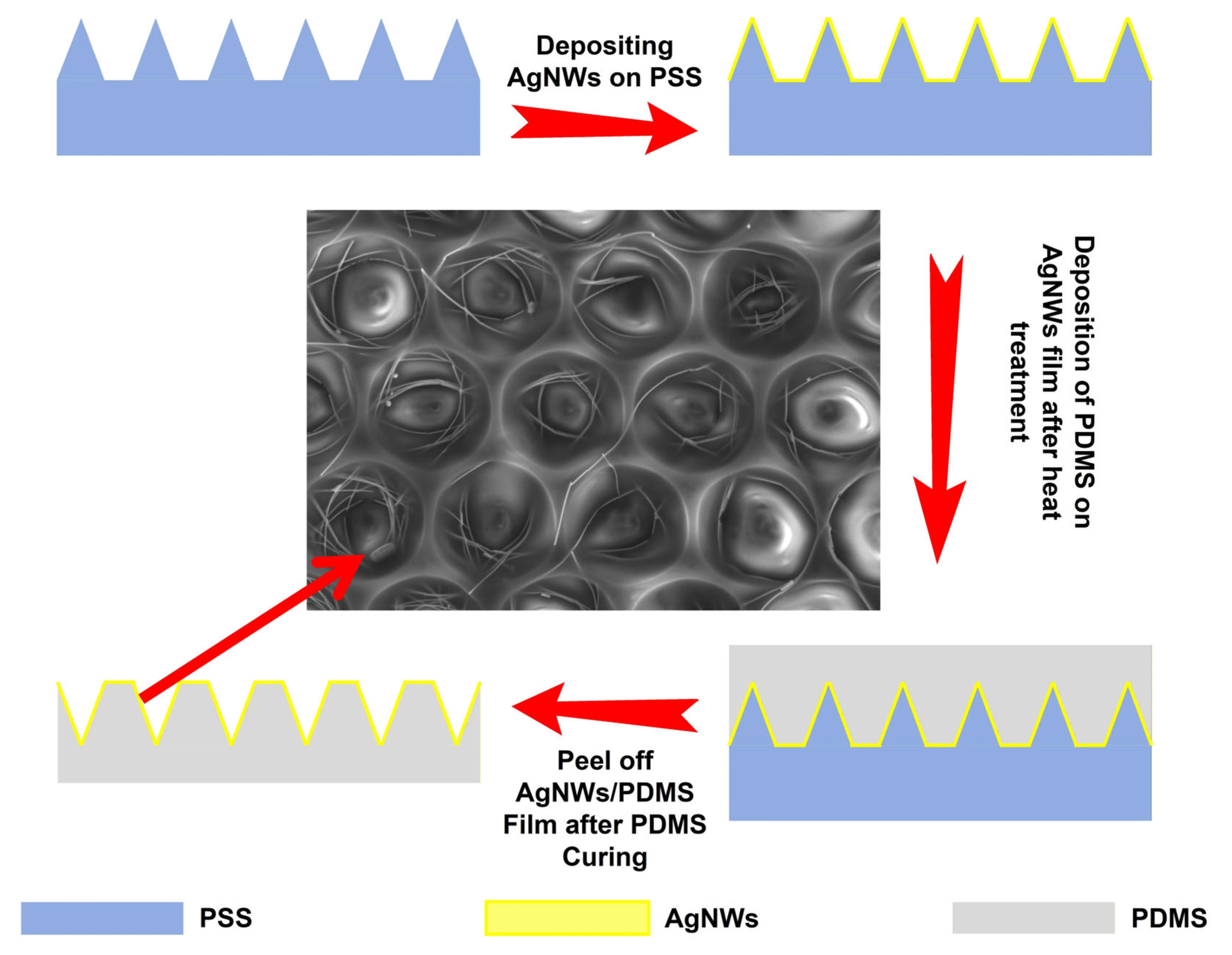
As shown in
Figure 1, first of all, the transparent conductive films of silver nanowires (AgNWs) were uniformly spin-coated on a patterned sapphire substrate (PSS). Silver nanowires play an important role in transparent conductive films due to their excellent conductivity, good optical transparency, and good flexibility, ensuring that the film not only has good conductivity but also effectively conducts and removes static electricity during the imprinting process. Next, a layer of liquid polydimethylsiloxane (PDMS) was coated on the surface of the AgNWs film. PDMS, as a highly elastic and insulating material, can not only increase the mechanical flexibility of the film but also serve as a protective layer to prevent damage during the imprinting process. After PDMS liquid coating, a uniform solid film was formed at 80 °C by heating and curing. After the curing process was completed, the entire transparent conductive film structure was easily peeled off from the PSS substrate using peeling technology. In this way, the AgNWs transparent conductive film was transferred to the PDMS surface along with the original graphic structure, forming a self-supporting transparent electrode with a three-dimensional structured surface.
3.2. Surface Characterization
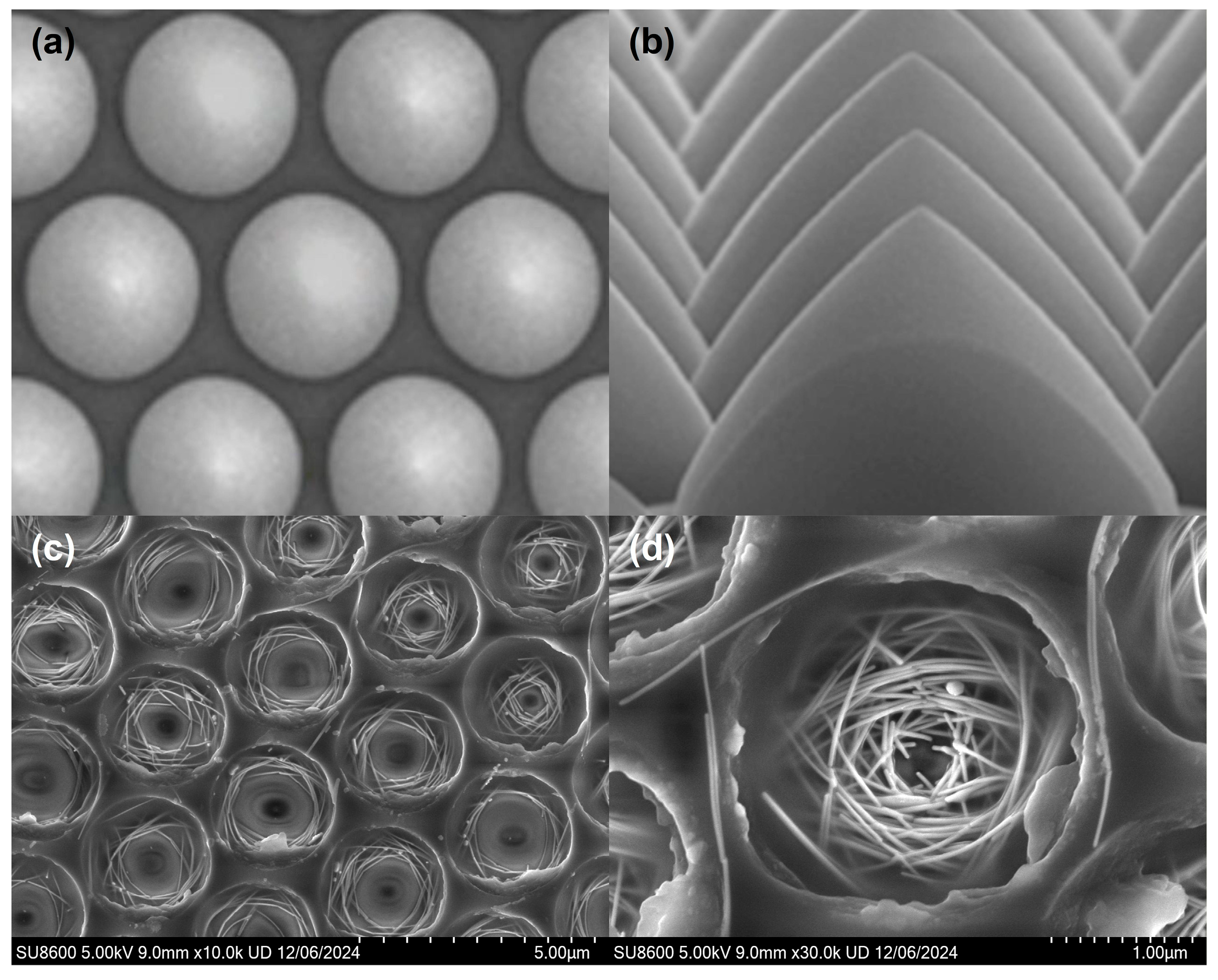
This study selected a patterned sapphire substrate (PSS) as the graphic template.
Figure 2a shows its front SEM image, and
Figure 2b shows its oblique SEM image, which clearly reveals the regular conical microstructure and periodic arrangement of the substrate surface. This provides a benchmark for subsequent comparative characterization of the surface morphology and pattern transfer effect of AgNWs/PDMS composite films through SEM. To further verify the surface morphology and microstructure of AgNWs/PDMS-based composite films, the research team used scanning electron microscopy (SEM) to observe the film surface in detail at different magnifications.
Figure 2c shows the surface morphology observed by SEM, which clearly illustrates the retention of the conical microstructure on the PSS substrate after transfer to the PDMS surface. It can be seen that the transferred PDMS surface formed circular pit structures corresponding to the PSS surface, with uniform spacing and good surface flatness, indicating that the process of pattern transfer was efficiently and accurately completed in the preparation of AgNWs/PDMS composite films. Further high-power magnification observation (as shown in
Figure 2d) revealed the embedding of silver nanowires (AgNWs) in the PDMS matrix. In this figure, AgNWs exhibit a clear linear distribution and are uniformly embedded in the microstructure of PDMS, forming a stable composite network. The high conductivity of silver nanowires combined with the elasticity of PDMS ensures that the composite film maintains good conductivity while possessing good flexibility and stability. Through SEM images, we could further confirm the uniform distribution and strong bonding of silver nanowires in PDMS substrates, which provides a reliable physical basis for subsequent electrostatic removal and nanoimprint lithography processes. These SEM characterization results demonstrate the successful preparation and excellent microstructure characteristics of the AgNWs/PDMS composite film, laying a solid foundation for its application in nanoimprint lithography.
3.3. Optoelectronic Properties
In order to evaluate the performance of AgNWs/PDMS-based composite films in practical applications, this study further investigated the UV transmittance and surface conductivity of the films.
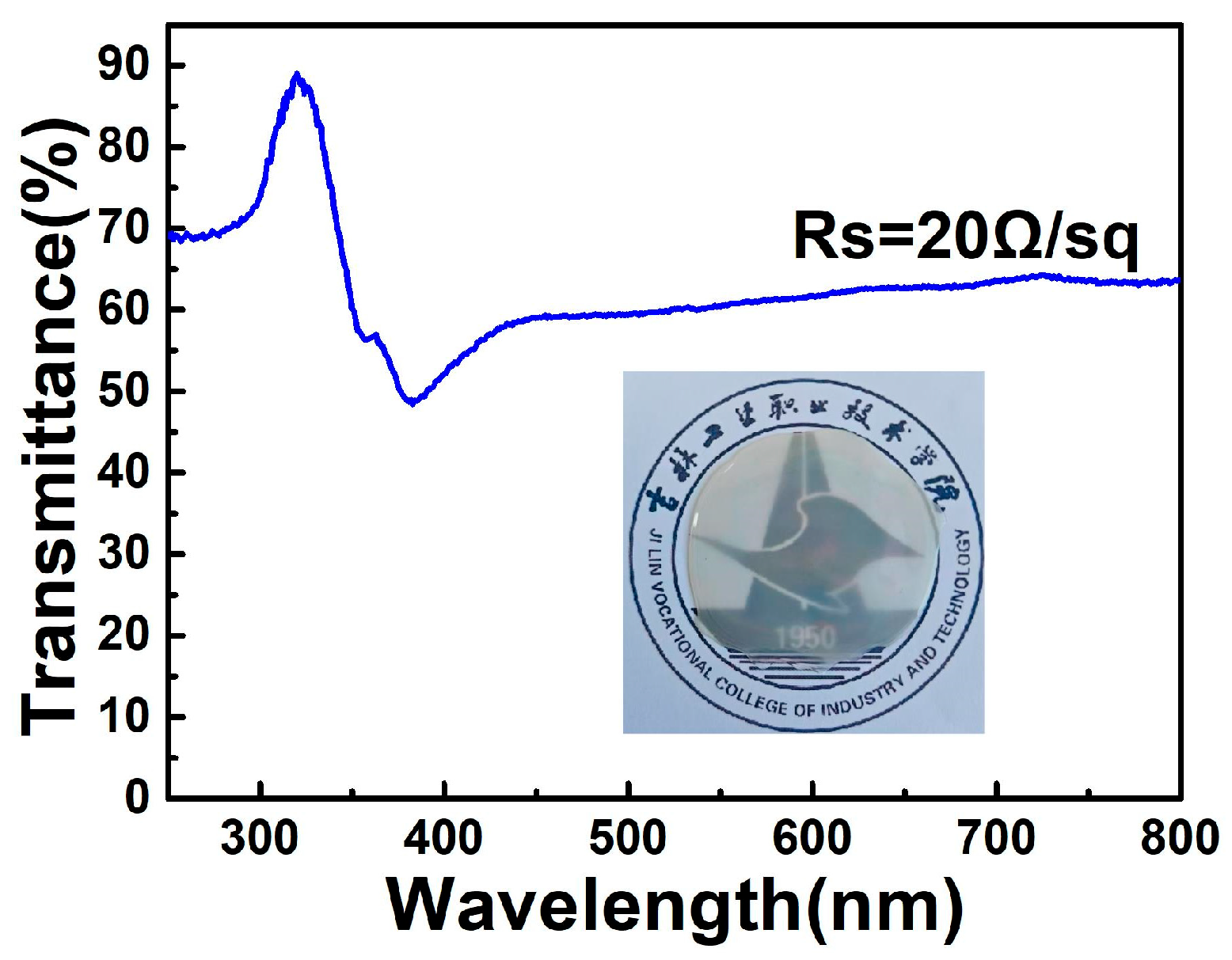
Figure 3 shows the transmittance data of the composite film under 325 nm wavelength ultraviolet light irradiation. The results show that the transmittance of the film at this wavelength can reach about 90%, which enables it to effectively transmit ultraviolet light to the target substrate during the nanoimprint lithography process, thereby ensuring the accuracy and efficiency of the imprinting process. The high transmittance of ultraviolet light is one of the key factors for the successful application of this composite film in the field of optoelectronics, especially in applications that require high-transparency materials, providing significant technological advantages. In addition, the measurement of the sheet resistance of the films showed that the composite film maintained a high UV transmittance while its sheet resistance was about 20 Ω/sq, indicating that the film had good conductivity. A lower sheet resistance value means that the films can effectively conduct electricity and quickly disperse and eliminate static electricity generated during the imprinting process. The accumulation of static electricity was mainly due to the concentration of surface charges on the material, and the conductive network of silver nanowires in the composite film provided an efficient charge conduction path, which could quickly dissipate and evenly distribute static electricity, thereby reducing the interference of static electricity on the imprinting process.
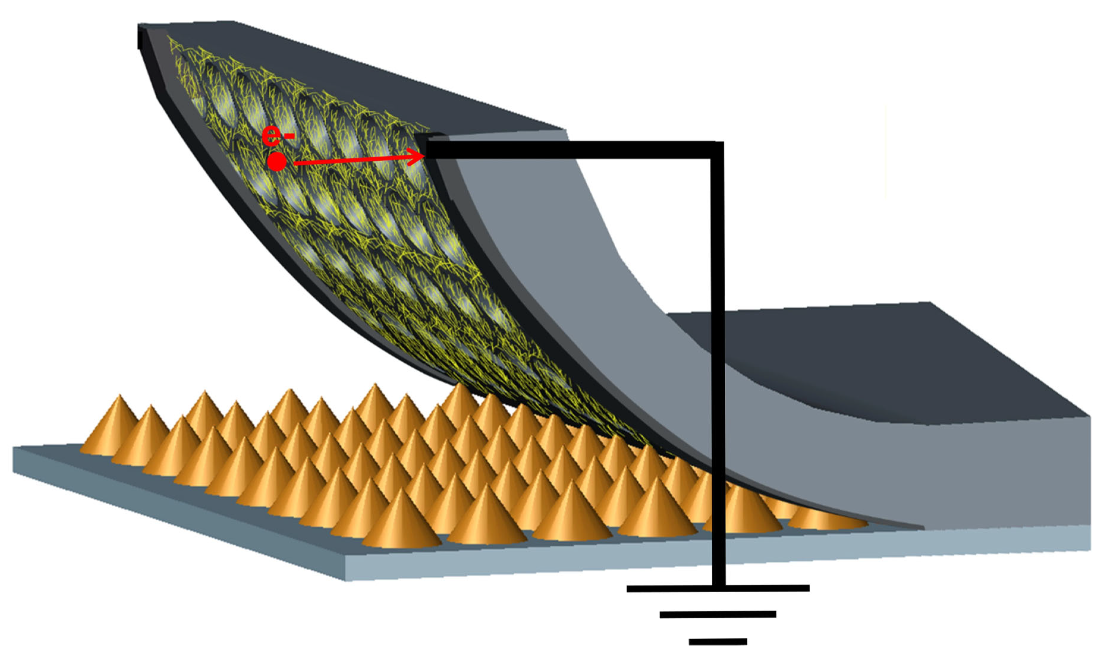
Embedding silver nanowires (AgNWs) into polydimethylsiloxane (PDMS) can construct a continuous flexible conductive network, effectively suppressing static accumulation and avoiding pattern distortion or equipment damage caused by static electricity during the nanoimprint lithography process. Nanoimprint contact separation and shear can lead to frictional electrification and charge injection, making it difficult to release in high-resistance polymers such as bare PDMS in a timely manner. Charge accumulates in local areas and generates a strong Coulomb attraction and electric field gradient. In the AgNWs/PDMS composite system, surface charges can rapidly diffuse laterally along the nanowire network and be dissipated through the grounding path with the mold/substrate or stage, significantly reducing the steady-state surface charge density (as shown in
Figure 4). In theory, the charge relaxation time can be approximated by the effective dielectric constant and effective conductivity (τ ≈ ε_eff/σ_eff). The extremely low conductivity of pure PDMS results in τ being on the order of minutes to hours, making it prone to sustained charging. After introducing an AgNWs network with a sheet resistance of approximately 20 Ω/sq, the σ_eff was increased by several orders of magnitude, reducing the τ to the millisecond level, allowing charges to be released within the generation scale [
24,
25,
26].
As shown in
Table 1, compared with traditional non-conductive polymer films such as PDMS, PET, and PVA, the AgNWs/PDMS composite film proposed in this work exhibits significant advantages in electrical and electrostatic management. This composite film achieves a low sheet resistance of approximately 20 Ω/sq, endowing the material with efficient electrostatic dissipation and ultrafast charge relaxation capabilities, thereby significantly reducing surface charge density and suppressing adhesion instability, pattern distortion, and defect generation caused by charge accumulation during the imprinting process. Mechanistically, the embedded silver nanowire network constructs a continuous conductive percolation channel and may undergo quantum tunneling and local plasmon coupling at the nanojunction, thereby improving the current-carrying and local electric field distribution. This is in sharp contrast to the electrostatic accumulation dominated by classical dielectric behavior in traditional dielectric films. Although the preparation of this composite film involves multi-step processes such as spin-coating, thermal curing, and delamination, compared to simple single-layer coating, it achieves effective synergy between conductivity and PDMS flexibility, significantly improving the graphic fidelity, process stability, and cross-sheet consistency of nanoimprint, and expanding its application range from low precision imprinting to high-precision nanoimprint and flexible optoelectronics.
3.4. Stability of the Films
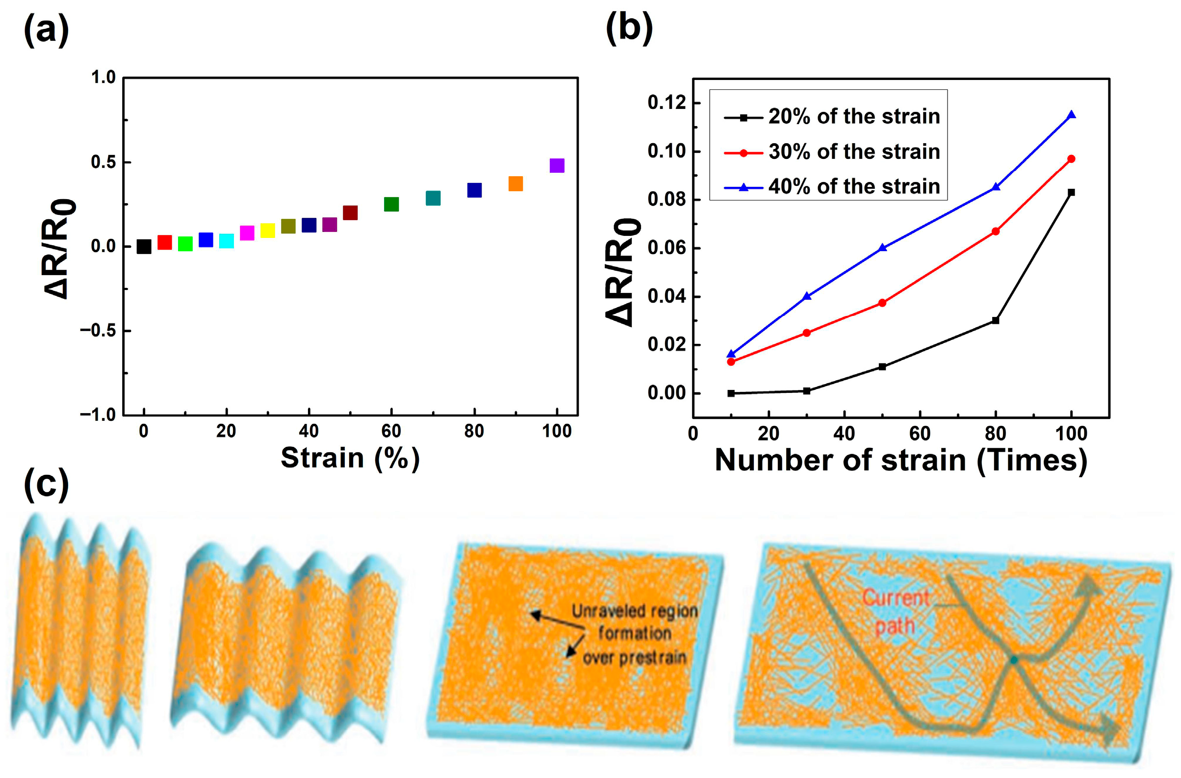
In the actual nanoimprint lithography process, the imprint film usually undergoes a certain degree of mechanical deformation. Therefore, whether the composite film can maintain stable conductivity during the deformation process is one of the key factors in evaluating its applicability. In order to verify the mechanical properties and conductivity stability of AgNWs/PDMS composite films, this study conducted systematic tensile tests on the composite films. The tests were conducted in a cleanroom simulation facility, maintaining a temperature range of 22 to 26 °C and a relative humidity level between 50% and 60%. The experimental results show that when the stretching amount does not exceed 20%, the conductivity of the composite film is almost unaffected, which far exceeds the common deformation range in the nanoimprint lithography process. In order to further evaluate the conductivity retention of the film under significant tensile deformation, we conducted 20%, 30%, and 40% tensile tests on the film and performed multiple cyclic tensile tests. The test results show that even when stretched up to 40%, the composite film’s sheet resistance only increases by about 12% after more than 100 repeated stretches, reaching 22.4 Ω/sq, and still maintains good conductivity, making it suitable for normal use. This indicates that the composite films have excellent tensile resistance and conductivity stability and can withstand a large degree of mechanical strain without affecting their functionality. As shown in
Figure 5c, the schematic diagram illustrates the evolution of the AgNWs conductive network within the PDMS matrix under tensile strain. After stretching, the expansion of the PDMS substrate leads to geometric sparsity of the embedded nanowire network, reducing the surface density of nanowires and the number of effective parallel conduction paths. This is conceptually similar to reducing the effective filler concentration to the percolation threshold, thereby increasing the overall network resistance. At higher strain levels, local stress concentration may further lead to the fracture of individual nanowires. These fractures cut off critical conductive pathways and created wider gaps, hindering the transmission of charges through tunneling, resulting in a more significant increase in resistance.
This experimental result indicates that the AgNWs/PDMS composite film not only maintains good conductivity during stretching but also exhibits strong durability and elasticity. The conductive network of silver nanowires in composite films can maintain an effective charge conduction pathway during tensile deformation, while the elasticity of PDMS ensures the mechanical strength and flexibility of the film. This enables the film to provide reliable performance support in applications, such as nanoimprint lithography, that require high flexibility and stability of the film, significantly improving its applicability and long-term performance in actual manufacturing processes.
4. Conclusions
This study successfully prepared AgNWs/PDMS-based three-dimensional structured surface transparent conductive thin films and explored their performance advantages in applications such as nanoimprint lithography. By embedding transparent electrodes into a transparent polymer substrate, this composite film maintains good optical transmittance while possessing efficient antistatic capabilities that traditional films do not possess. In terms of ultraviolet light transmittance, the film exhibits excellent light transmittance performance, especially reaching about 90% at a wavelength of 325 nm, which enables it to effectively transmit ultraviolet light and meet the lighting requirements of nanoimprint lithography. At the same time, the conductivity of the composite film is excellent, and the sheet resistance as low as 20 Ω/sq can effectively eliminate the accumulation of static electricity during the nanoimprint process, avoiding the impact of static electricity on pattern transfer and equipment safety. In terms of mechanical properties, the tensile strength of the composite film was further verified through tensile testing. Even when stretched beyond 40%, the conductivity of the film remains stable, and the sheet resistance only increases by about 12%, indicating that it can still maintain high stability and durability under large deformations. This excellent tensile resistance makes the film have broad application prospects in flexible electronics and other high-strain environments. Overall, the AgNWs/PDMS composite film demonstrates a unique combination of high UV transmittance, moderate electrical conductivity, and excellent mechanical stretchability. This set of properties makes it a promising candidate material for addressing the electrostatic issue in NIL. The charge dissipation capability is derived from its conductivity, and its stability under strain supports use in flexible imprinting contexts. Future work involving direct charge decay measurements and NIL process benchmarking will be crucial to fully validate its practical efficacy.
Author Contributions
Conceptualization, Y.C., X.Z. (Xiaohua Zhao), X.Z. (Xuetao Zhang), Z.Y. and D.M.; Methodology, Y.C., X.Z. (Xiaohua Zhao), Z.Y. and D.M.; Formal analysis, X.Z. (Xiaohua Zhao); Investigation, X.Z. (Xuetao Zhang) and Z.Y.; Resources, Y.C. and Z.Y.; Writing—original draft, Y.C., X.Z. (Xuetao Zhang) and Z.Y.; Writing—review & editing, Y.C. and Z.Y.; Project administration, Y.C.; Funding acquisition, Y.C. and D.M. All authors have read and agreed to the published version of the manuscript.
Funding
This research was supported by Jilin Province Young Scientific and Technological Talents Training Project (Grant No.: 20250602039RC).
Institutional Review Board Statement
Not applicable.
Informed Consent Statement
Not applicable.
Data Availability Statement
The data that support the findings of this study are available from the corresponding author upon reasonable request.
Conflicts of Interest
The authors declare that they have no known competing financial interests or personal relationships that could have appeared to influence the work reported in this paper.
References
- Lee, S.-M.; Biswas, R.; Li, W.; Kang, D.; Chan, L.; Yoon, J. Printable nanostructured silicon solar cells for high-performance, large-area flexible photovoltaics. ACS Nano 2014, 8, 10507–10516. [Google Scholar] [CrossRef]
- Woo, J.Y.; Jo, S.; Oh, J.H.; Kim, J.T.; Han, C.-S. Facile and precise fabrication of 10-nm nanostructures on soft and hard substrates. Appl. Surf. Sci. 2019, 484, 317–325. [Google Scholar] [CrossRef]
- Qiu, M.; Du, W.; Zhou, S.; Cai, P.; Luo, Y.; Wang, X.; Yang, R.; Zhao, J. Recent progress in non-photolithographic patterning of polymer thin films. Prog. Polym. Sci. 2023, 142, 101688. [Google Scholar] [CrossRef]
- Lim, H.J.; Lee, J.J.; Choi, K.B.; Kim, G.H.; Ahn, H.J.; Ryu, J.H. UV/Thermal Hybrid Nanoimprint System for Flexible Substrates. J. Korean Soc. Manuf. Technol. Eng. 2011, 20, 245–250. [Google Scholar]
- Yun, H.-W.; Choi, G.-M.; Woo, H.K.; Oh, S.J.; Hong, S.-H. Superhydrophobic, antireflective, flexible hard coatings with mechanically ultra-resilient moth-eye structure for foldable displays. Curr. Appl. Phys. 2020, 20, 1163–1170. [Google Scholar] [CrossRef]
- Frolet, N.; Durret, J.; Panabière, M.; Boisseau, S.; Gourgon, C. Impact of surface electrostatic potential on icephobic properties of nanoimprinted flexible polymer foils. Macromol. Chem. Phys. 2018, 219, 1800070. [Google Scholar] [CrossRef]
- Lee, H.; Kim, H.J. Nanoimprinting of perovskite layer for light-harvesting effect in photovoltaic devices. Electron. Mater. Lett. 2022, 18, 407–414. [Google Scholar] [CrossRef]
- Kim, D.H.; Lee, D.W.; Oh, J.Y.; Won, J.; Liu, Y.; Seo, D.S. Self aligned liquid crystals on sol-gel-processed zirconium oxide surface via nanoimprinting lithography. Opt. Mater. 2022, 129, 112494. [Google Scholar] [CrossRef]
- Zhou, H.; Mao, H.; Meng, X.; Wang, Q.; Tan, L.; Chen, Y. Electroless deposition of silver grids flexible transparent electrode integrated by ultra-violet nanoimprint lithography. Org. Electron. 2019, 75, 105408. [Google Scholar] [CrossRef]
- Sun, Y.-K.; Wang, L.; Kamano, M.; Juodkazis, S. Plasmonic nano-imprinting by photo-doping. Opt. Lett. 2018, 43, 3786–3789. [Google Scholar] [CrossRef]
- Salunke, M.; Viswalingam, V.; Shinde, V. Electrospun nanofibers of carbohydrate polymers for neoteric wound dressing: A review. Int. J. Polym. Mater. Polym. Biomater. 2025, 74, 103–127. [Google Scholar] [CrossRef]
- Jeong, W.-H.; Kim, H.; Kansara, S.; Lee, S.; Agostini, M.; Kim, K.; Hwang, J.-Y.; Jung, Y.-C. Stimulating the electrostatic interactions in composite cathodes using a slurry-fabricable polar binder for practical all-solid-state batteries. Energy Storage Mater. 2024, 73, 103855. [Google Scholar] [CrossRef]
- Li, X.; Liu, S.; Meng, X.; Zhang, S.; Yu, M.; Wu, L.; Liang, X. Modified antistatic carbonaceous fiber with excellent hydrophobicity, environmental stability and radar absorption performance. Carbon 2024, 229, 119501. [Google Scholar] [CrossRef]
- Huang, W.; Yu, X.; Liu, Y.; Qiao, W.; Chen, L. A review of the scalable nano-manufacturing technology for flexible devices. Front. Mech. Eng. 2017, 12, 99–109. [Google Scholar] [CrossRef]
- Vitukhnovskii, A.G.; Kolesnikov, A.O.; Kolymagin, D.A.; Ragozin, E.N.; Shatokhin, A.N. 3D Laser Lithography Technique in the Fabrication of a Coherent 2D Kinoform X-ray Lens. Bull. Lebedev Phys. Inst. 2024, 51, S424–S433. [Google Scholar] [CrossRef]
- Lan, W.; Chen, Y.; Yang, Z.; Han, W.; Zhou, J.; Zhang, Y.; Wang, J.; Tang, G.; Wei, Y.; Dou, W.; et al. Ultraflexible transparent film heater made of Ag nanowire/PVA composite for rapid-response thermotherapy pads. ACS Appl. Mater. Interfaces 2017, 9, 6644–6651. [Google Scholar] [CrossRef]
- Lan, W.; Yang, Z.; Zhang, Y.; Wei, Y.; Wang, P.; Abas, A.; Tang, G.; Zhang, X.; Wang, J.; Xie, E. Novel transparent high-performance AgNWs/ZnO electrodes prepared on unconventional substrates with 3D structured surfaces. Appl. Surf. Sci. 2018, 433, 821–828. [Google Scholar] [CrossRef]
- Yang, Z.; Zhao, H.; Qi, X.; Yao, C.; Ma, R.; Song, J.; Cao, Y.; Ma, D.; Li, H.; Cui, G.; et al. Novel ultraflexible transparent self-heating composite films for nanoimprint lithography. Mater. Des. 2025, 254, 114123. [Google Scholar] [CrossRef]
- Ahmad, Z.; Parias M. R, B.; Barr, H.; Cabral, J.T. Thermal Conduction Suppresses Cracks in PDMS Wrinkling by Plasma Oxidation. Nano Lett. 2024, 25, 740–746. [Google Scholar] [CrossRef]
- Wen, S.; Zhang, R.; Zhao, Y.; Xu, X.; Ji, S. Patterning Adhesive Layers for Array Electrodes via Electrochemically Grafted Polymers. ACS Omega 2025, 10, 3190–3198. [Google Scholar] [CrossRef]
- Firdous, I.; Fahim, M.; Lin, K.; Ho, T.C.; Zhu, Y.; Tso, C.Y. Electragel for Advanced Static Charge Mitigation and Energy Harvesting. Adv. Sci. 2025, 12, e04600. [Google Scholar] [CrossRef] [PubMed]
- Zhong, H.; Meng, T.; Ding, W.; Xiao, Y.; Zhang, P. Achieving a Porous PDMS Film for Passive Cooling through the Utilization of Ultrafine NaCl Sacrificial Template. ACS Omega 2024, 10, 1012–1018. [Google Scholar] [CrossRef] [PubMed]
- Nguyen, V.H.; Papanastasiou, D.T.; Resende, J.; Bardet, L.; Sannicolo, T.; Jiménez, C.; Muñoz-Rojas, D.; Nguyen, N.D.; Bellet, D. Advances in Flexible Metallic Transparent Electrode. Small 2022, 18, 2106006. [Google Scholar] [CrossRef]
- Halder, P.; Ali, M.S.; Chattopadhyay, D.; Bhattacharya, S. Dielectric properties, relaxation time and conduction behavior of MoO3 doped V2O5-ZnO-CuO glassy semiconducting system. Appl. Phys. A 2024, 130, 621. [Google Scholar] [CrossRef]
- Gentili, D.; Calabrese, G.; Lunedei, E.; Borgatti, F.; Mirshokraee, S.A.; Benekou, V.; Tseberlidis, G.; Mezzi, A.; Liscio, F.; Candini, A.; et al. Tuning Electronic and Functional Properties in Defected MoS2 Films by Surface Patterning of Sulphur Atomic Vacancies. Small Methods 2024, 9, e2401486. [Google Scholar] [CrossRef]
- Jacobs, H.O.; Whitesides, G.M. Submicrometer patterning of charge in thin-film electrets. Science 2001, 291, 1763–1766. [Google Scholar] [CrossRef] [PubMed]
| Disclaimer/Publisher’s Note: The statements, opinions and data contained in all publications are solely those of the individual author(s) and contributor(s) and not of MDPI and/or the editor(s). MDPI and/or the editor(s) disclaim responsibility for any injury to people or property resulting from any ideas, methods, instructions or products referred to in the content. |
