Article

Effect of Indium Doping on the Photoelectric Properties of SnS Thin Films and SnS/TiO2 Heterojunctions

Department of Materials Science, Fudan University, Shanghai 200433, China
*
Author to whom correspondence should be addressed.
Coatings 2025, 15(8), 972; https://doi.org/10.3390/coatings15080972
Submission received: 21 July 2025 / Revised: 12 August 2025 / Accepted: 19 August 2025 / Published: 20 August 2025
(This article belongs to the Special Issue Electrochemical Properties and Applications of Thin Films)

Abstract

This study addresses the need for efficient photoelectric materials by fabricating Indium-doped tin sulfide (SnS-In)/titanium dioxide (TiO2) heterostructure thin films via radio frequency (RF) magnetron sputtering. We systematically investigated the synergistic enhancement of photoelectric properties from both In-doping and the heterostructure design. SnS-In films with controlled In concentrations were prepared by embedding varying numbers of indium pellets into the SnS sputtering target. Our findings reveal that an optimal In doping of 4.93 at% significantly improves the crystalline quality and light absorption of SnS, reducing its band gap from 1.27 eV to 1.13 eV and enhancing carrier concentration and mobility. Subsequently, the optimized SnS-In film combined with TiO2 formed a heterojunction, achieving a peak photocurrent density of 6.36 µA/cm2 under visible light. This is 2.2 and 53.0 times higher than standalone SnS-In and TiO2 films, respectively. This superior performance is attributed to the optimal In3+ doping effectively modulating the SnS band structure and the type-II heterojunction promoting efficient charge separation. This work demonstrates a promising strategy for optoelectronic conversion and photocatalysis by combining In-doping for SnS band structure engineering with TiO2 heterostructure construction.

Graphical Abstract

1. Introduction

Tin(II) sulfide (SnS) is a promising material for diverse optoelectronic applications due to its broad light absorption range, particularly its excellent absorption in the visible and near-infrared regions [1,2,3]. This property makes it highly suitable for photocatalysis, sensors [4], and solar cells [5,6]. Enhancing the performance of SnS is crucial for advancing these technologies. Doping stands out as an effective strategy to tune the band gap, carrier concentration, and other physicochemical properties of SnS, thereby improving its optoelectronic device performance [7].
Researchers commonly employ both metallic and non-metallic elements as dopants. Metallic dopants include Ag [8], Cu [9], Zn [10], Sb [11], In [12], and Bi [13]. For instance, Bommireddy et al. demonstrated that moderate Cu doping (2–4%) in SnS thin films improved crystallinity, induced a red shift in the absorption edge, and reduced the band gap, significantly increasing carrier concentration and decreasing resistivity [9]. Similarly, Dussan et al. reported that Bi doping enhanced the electrical conductivity of SnS films and could even induce a transition from p-type to n-type conductivity at higher concentrations [13]. Non-metallic dopants, such as P [14], Cl [15], and Br [16], have also been explored. Kawanishi et al. found that Cl and Br doping increased grain size and shifted the Fermi level upward, resulting in n-type SnS semiconductors with significantly improved electrical conductivities and carrier concentrations [15].
Among the various dopants, Indium (In) is particularly attractive. Located near Sn in the periodic table, In possesses a suitable atomic radius and electronic structure that facilitates its substitution for Sn atoms within the SnS crystal lattice [12]. Compared to other Group III elements like Al and Ga, In exhibits lower reactivity with oxygen, better electrical conductivity, and enhanced chemical stability, making it an ideal candidate for property modulation [17]. Numerous studies have confirmed that In-doping effectively tunes the optoelectronic properties of SnS. For example, Abd El-Hady et al. observed that In-doping improved crystalline quality, reduced the optical band gap (from 1.32 eV to 1.25 eV), broadened spectral absorption, and drastically increased electrical conductivity by four orders of magnitude due to enhanced carrier concentration [18]. Similarly, Khan et al. reported significant improvements in the electrical and optical properties of SnS-In films, noting that the substitution of Sn2+ by In3+ ions provided additional free electrons, leading to a dramatic reduction in resistivity from 105 Ω·cm to 10−2 Ω·cm and promoting n-type semiconductor characteristics [19]. These enhanced electrical properties underscore the potential of In-doped SnS for efficient optoelectronic devices [20]. However, there are limited reports on the preparation of In-doped SnS films using magnetron sputtering, a highly controllable and scalable deposition technique.
Despite its promising light-harvesting capability, pristine SnS suffers from inherently low photoconductivity and severe recombination of photogenerated charge carriers, which significantly limits its photoelectric conversion efficiency. Constructing a heterojunction with a wide-bandgap n-type semiconductor such as TiO2 has emerged as an effective strategy to overcome these limitations. Through proper band alignment (Type-II configuration), photogenerated electrons in SnS can transfer to TiO2, while holes remain in SnS, achieving spatial separation of charge carriers and suppressing recombination. This interfacial effect is crucial for enhancing carrier extraction and improving overall photo response.
Building upon our previous work on magnetron sputtering fabrication of SnS thin films and SnS/TiO2 heterostructures [21], this study aims to investigate the synergistic effects of In-doping on the photoelectric properties of both SnS films and SnS-In/TiO2 heterojunctions. We specifically focus on understanding the underlying mechanisms responsible for the observed performance enhancements, demonstrating the potential of this integrated approach for advanced optoelectronic conversion.

2. Materials and Methods

2.1. Material Preparation

In this experiment, SnS-In films with varying doping concentrations were prepared by embedding different numbers of high-purity indium (In) pellets into the sputtering area of an SnS target. The SnS target (purity: 99.99%) was purchased from Zhongnuo Advanced Materials (Beijing) Co., Ltd. (Beijing, China), with a diameter of 60 mm and a thickness of 3 mm. Although the exact density of the target was not specified by the supplier, it was fabricated by hot pressing. The indium pellets (purity: 99.995%, size: 1–3 mm) were symmetrically embedded along the erosion ring of the SnS target to ensure uniform in situ doping during sputtering. The TiO2 target also had a purity of 99.99%.
The sputtering was performed in high-purity argon gas (99.999%) at a working pressure of 0.55 Pa. The base pressure before deposition was below 2.5 × 10⁻³ Pa. The films for general characterization were deposited on soda-lime glass substrates, while those used for photoelectric measurements were grown on FTO conductive glass. Radio frequency (RF) magnetron sputtering was carried out at a power of 80 W, a substrate temperature of 200 °C, and a target-to-substrate distance of 6 cm. The deposition time was fixed at 20 min. After deposition, all films were annealed in Ar at 300 °C for 1 h. The In doping concentration was controlled by varying the number of In pellets embedded in the target. Samples prepared with 2, 4, and 6 pellets were denoted as In(1), In(2), and In(3), respectively, while the undoped reference sample was labeled In(0).
The SnS film exhibited optimal photoelectric properties at an In doping concentration of 4.93 at% (corresponding to the In(2) sample). Based on this optimization, SnS-In/TiO2 bilayer films were prepared. First, a TiO2 layer was deposited onto the substrate by magnetron sputtering at a power of 300 W for 30 min, followed by annealing at 500 °C for 2 h. Next, with 4 In pellets embedded in the SnS target, an SnS-In layer was deposited onto the TiO2 layer at a sputtering power of 80 W. The sputtering time was varied (8 min, 12 min, 16 min, and 20 min) to obtain SnS-In layers of different thicknesses. Finally, the fabrication of the SnS-In/TiO2 bilayer films was completed by annealing at 300 °C for 1 h in an Ar atmosphere.

2.2. Analysis and Testing

The crystal structure and phase composition of the samples were characterized using an X-ray diffractometer. The surface and cross-sectional morphologies of the films were analyzed by scanning electron microscopy and atomic force microscopy. The elemental composition and chemical valence states of the films were determined using X-ray photoelectron spectroscopy. Raman spectroscopy was carried out using a LabRAM HR Evolution Raman spectrometer. A 532 nm laser was used for excitation, with the laser power controlled below 1 mW to prevent thermal effects on the sample surface. The system provides a spectral resolution better than 0.5 cm−1. Each spectrum was acquired with an integration time of 10 s, and 3 accumulations were used to improve the signal-to-noise ratio. The optical absorption properties were evaluated using a UV-Vis-NIR spectrophotometer.
The thickness of the thin films was measured using a surface profilometer, which provides a vertical resolution of 0.38 Å, a maximum measurement range of 1000 μm, and a precision up to 5 Å. Its dual-detector design ensures high resolution even over large scan lengths. To account for potential thickness non-uniformity, at least five different positions were randomly selected and scanned on each sample. The reported values represent the average thickness, with the standard deviation typically within ±5 nm. Considering both instrumental resolution and inter-point variation, the overall uncertainty is estimated to be within ±10 nm. These procedures ensure the reliability of the reported thickness data.
Hall effect measurements were performed to characterize the electrical properties of the semiconductor materials. This technique determines the material’s conductivity type (n-type or p-type), carrier concentration, resistivity, and Hall mobility by measuring the Hall voltage induced when a current-carrying sample is subjected to a perpendicular magnetic field.
All photoelectric (PEC) measurements were performed at room temperature on an electrochemical workstation (CHI660E) using a standard three-electrode system. In this system, the film sample deposited on FTO conductive glass (effective area: 1 cm2) served as the working electrode, a saturated calomel electrode (SCE) was used as the reference electrode, and a platinum disk electrode acted as the counter electrode. A xenon lamp was used as the light source, and a filter was employed to control the visible light wavelength to the 420–780 nm range. The light irradiation intensity on the sample surface was 62 mW/cm2. The electrolyte was a 0.5 mol/L aqueous solution of Na2SO4 (pH = 7). All measured potentials were converted to the reversible hydrogen electrode (RHE) scale using the Nernst equation (Equation (1)) [22]:
E R H E = E S C E + 0.0591 p H + E S C E θ E S C E θ = 0.2415   vs .   NHE   at   25   C
where ERHE is the potential on the RHE scale, ESCE is the measured potential against the saturated calomel electrode (SCE), pH is the pH of the electrolyte, and E S C E θ is the standard potential of the SCE (0.2415 V vs. NHE at 25 °C). Transient photocurrent measurements were conducted at open-circuit potential by recording the current-time (I-t) curves under alternating light-on and light-off conditions. The interval for both light-on and light-off periods was 50 s, with a total test duration of 400 s. Electrochemical impedance spectroscopy (EIS) tests were performed under visible light illumination over a scanning frequency range of 0.1 Hz to 100,000 Hz. Mott–Schottky analysis was conducted in the dark at a fixed frequency of 1000 Hz with an AC amplitude of 10 mV.

3. Results

3.1. Modulation of Microstructure and Photoelectric Properties of SnS Thin Films by In-Doping

3.1.1. Crystal Structure and Phase Analysis

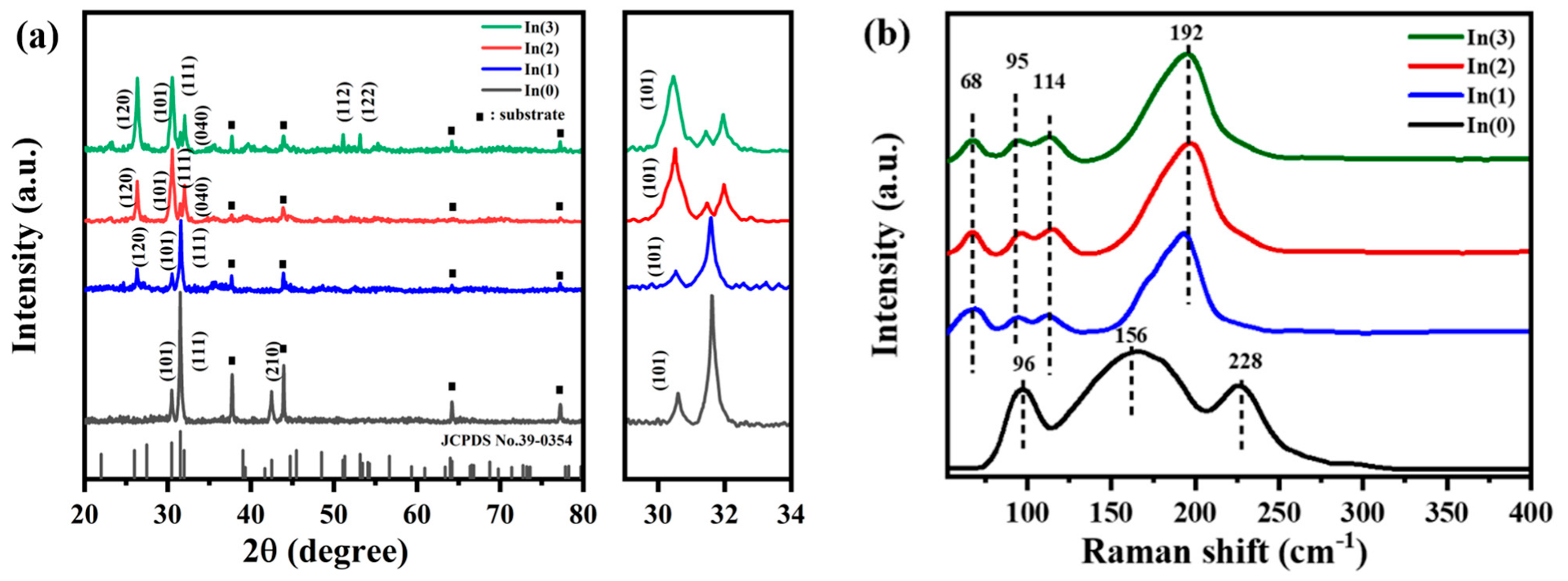
Figure 1a shows the XRD patterns of the SnS thin films with different In doping concentrations. All patterns are consistent with the standard data for orthorhombic SnS (JCPDS No. 39-0354), indicating that the films maintained a pure SnS phase structure. The pure SnS film exhibits a mixed orientation along the (111) and (101) crystallographic planes. Upon the introduction of a small amount of In (the In(1) sample), the preferred orientation of the film shifts to the (101) and the newly emerged (120) planes. As the In concentration increases, the diffraction intensities of the (101) and (120) planes continually intensify, while the intensity of the (111) peak sharply diminishes. This is accompanied by the appearance of new diffraction peaks, such as (040), (112), and (122). This indicates that In-doping induces a change in the preferred orientation of the SnS films from the (111) direction to the (101) and (120) directions.
To quantitatively assess this evolution of crystallographic orientation, we calculated the texture coefficient (TC) values for the main diffraction planes using the following equation (Equation (2)):
T C ( h k l ) = I ( h k l ) / I 0 ( h k l ) 1 N n = 1 N I ( n ) / I 0 ( n )
where I(hkl) and I0(hkl) represent the measured and standard intensities of the (hkl) plane, respectively. Due to the use of a single sample, standard deviations are not available.
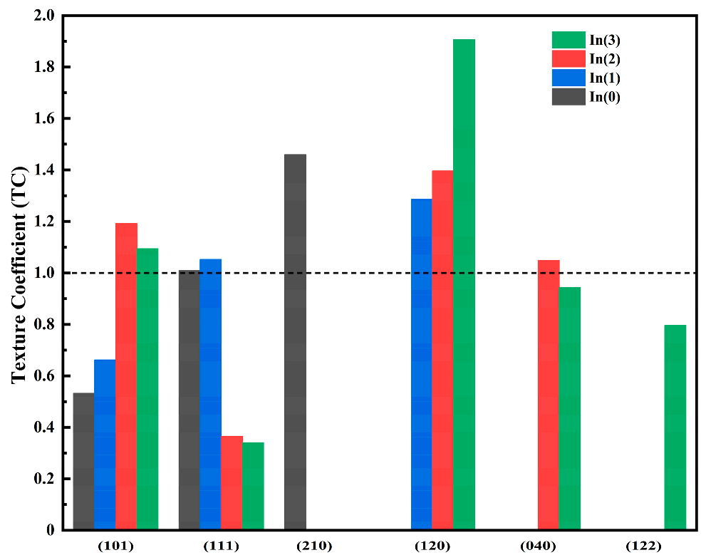
The calculated TC values are summarized in Figure 2. For the undoped SnS (In(0)), the (111) and (101) planes exhibit nearly comparable TC values, indicating a mixed orientation. With increasing In doping, the TC of the (101) and (120) planes increases significantly, while that of the (111) plane decreases rapidly, confirming the doping-induced reorientation of the crystalline structure. These results provide solid quantitative evidence supporting the shift in preferred growth direction.
More importantly, the positions of the main diffraction peaks, such as the (101) peak, systematically shift to lower angles with increasing In content. This phenomenon of lattice expansion is consistent with Vegard’s law, confirming that In3+ ions successfully substituted Sn2+ ions in the SnS lattice, leading to lattice distortion [23].
The grain size (D) and microstrain (ε) of the SnS-In films were calculated using the Scherrer equation (Equation (3)) and the strain equation (Equation (4)), respectively [24,25]:
D = K λ β c o s θ
ε = β 4 t a n θ
where K is the Scherrer constant, λ is the X-ray wavelength (0.15406 nm), β is the full width at half maximum (FWHM) of the diffraction peak, and θ is the Bragg diffraction angle.
The lattice constants of the films were calculated using the Bragg equation (Equation (5)) and the interplanar spacing formula for an orthorhombic system (Equation (6)):
λ = 2 d h k l s i n θ
1 d h k l 2 = h a 2 + k b 2 + l c 2
The unit cell volume was calculated using Equation (7) [26,27]:
V = a · b · c
where λ is the wavelength of the incident X-ray, dhkl is the interplanar spacing, θ is the diffraction angle, (h, k, l) are the Miller indices, and (a, b, c) are the lattice constants.
To investigate the effect of In-doping on the crystalline quality of the SnS thin films, a detailed analysis of the XRD patterns was conducted, with the key calculation results summarized in Table 1. As shown in Figure 1a, the diffraction peaks, particularly the (101) and (120) planes, exhibit a clear broadening trend with increasing In doping concentration. Calculations using the Scherrer equation reveal that the average grain size of the films significantly decreases from 27.5 nm for the undoped sample to 21.1 nm for the In(3) sample. Concurrently, the lattice microstrain monotonically increases from 4.29 × 10⁻³ to 7.36 × 10⁻³. The decrease in grain size and the increase in strain collectively cause a broadening of the diffraction peaks, which in turn leads to a reduction in their intensity for the doped samples. This suggests that the incorporation of In atoms into the SnS lattice introduces more crystal defects and increases lattice distortion, which, to some extent, inhibits the preferred growth of grains and reduces the crystalline quality of the films [28].
The change in diffraction peak positions further reveals the mode of In’s existence within the crystal lattice. We precisely calculated the lattice constants and unit cell volume of the samples (Table 2). The results show that, compared to the pure SnS film (1.957 × 10⁻²⁸ m3), the unit cell volume of the In-doped samples systematically decreases to approximately 1.91 × 10⁻²⁸ m3. This phenomenon of unit cell contraction is in complete agreement with the ionic radii difference between In3+ (0.80 Å) and Sn2+ (0.93 Å). When smaller In3+ ions successfully substitute for larger Sn2+ ions, it inevitably leads to a change in lattice constants and a contraction of the unit cell volume [23]. All quantitative parameters with deviations (e.g., crystallite size, strain, and dislocation density) were calculated based on the average of at least three measurements, and the errors represent one standard deviation (±SD). XRD-derived parameters were averaged from multiple diffraction peaks to minimize orientation bias and ensure consistency.
To further corroborate the lattice distortion caused by In-doping, Raman spectroscopy analysis was performed, as shown in Figure 1b. The pure SnS film exhibits clear characteristic vibrational modes at 96 cm−1 (Ag), 156 cm−1 (B3g), and 228 cm−1 (Ag). After In-doping, the Raman spectrum changes significantly: the original phonon modes at 156 cm−1 and 228 cm−1 disappear, while new vibrational peaks emerge at 68 cm−1 (B2g), 114 cm−1 (Ag), and 192 cm−1 (Ag) [12,29]. This reconstruction of vibrational modes is due to the substitutional In3+ ions altering the local lattice symmetry and interatomic interaction forces, thereby triggering a change in phonon scattering behavior [29].
Combining the XRD and Raman analyses, it can be concluded that In atoms have been successfully incorporated into the SnS lattice via substitution. Although In-doping led to grain refinement, increased strain, and altered lattice vibrational modes, it did not introduce any detectable impurity phases, thus laying a structural foundation for subsequent performance modulation.

3.1.2. Surface Morphology Analysis

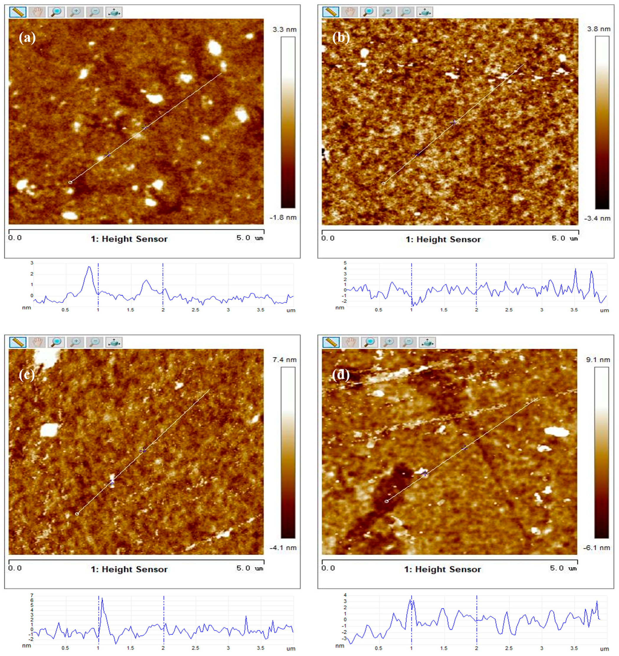
To study the effect of In-doping on the surface morphology and roughness of the thin films, AFM tests were conducted, and the three-dimensional morphologies are shown in Figure 3. It can be visually observed that the surface of the pure SnS film is composed of relatively large, well-defined grains, resulting in a relatively smooth surface. With the incorporation of In, the grain size on the film surface gradually becomes finer, and the morphology becomes more compact. This phenomenon is in complete agreement with the trend of decreasing grain size observed in the XRD analysis, further confirming that the lattice distortion and increased defects caused by the substitution of Sn2+ by In3+ are the core mechanisms for modulating the film’s microstructure.
The quantitative analysis of the surface morphology further supports these observations. The root-mean-square (RMS) roughness (Rq) of the films was calculated from a central 3.5 × 3.5 μm2 area of the 2D scans and is found to monotonically increase with the In-doping concentration. Specifically, the Rq value for the pure SnS film is 0.64 nm, whereas for the In(1), In(2), and In(3) samples, this value increases to 1.18 nm, 1.70 nm, and 1.93 nm, respectively. This increase in surface roughness is a direct macroscopic manifestation of grain refinement and enhanced crystallographic irregularity. In other words, the lattice stress introduced by doping not only restricts the two-dimensional planar growth of the grains but also promotes three-dimensional island-like nucleation, thereby leading to a systematic degradation of the film’s surface smoothness.

3.1.3. Elemental Composition Analysis

EDS and XPS tests were conducted on the SnS-In thin film samples with different In doping concentrations.
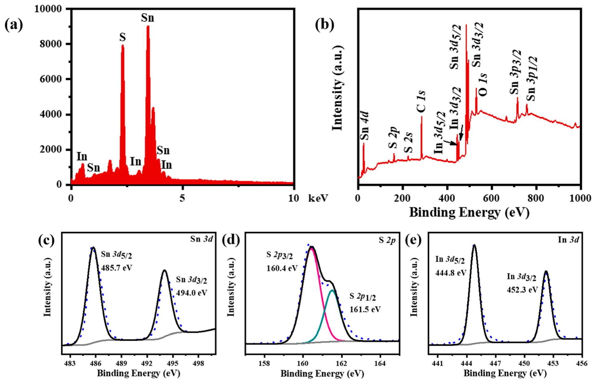
First, we performed a quantitative analysis of the elemental composition and doping level of the films using EDS (Figure 4a), with the results summarized in Table 3. The data show that the actual atomic percentages of In in the In(1), In(2), and In(3) samples are 2.78 at.%, 4.93 at.%, and 6.06 at.%, respectively, which positively correlates with the number of In sources set during preparation. This not only proves that the In doping concentration can be effectively controlled by this method but also establishes the compositional foundation for subsequent performance studies. More importantly, the data indicate that an increase in the atomic percentage of In is always accompanied by a corresponding decrease in the atomic percentage of Sn, which provides an initial hint of a substitutional doping mechanism of In for Sn.
To further confirm the chemical valence states of the elements and the doping mechanism of In, XPS tests were conducted on samples with different In doping concentrations. As no significant differences were found, the representative In(2) sample was chosen for detailed analysis. The XPS survey spectrum in Figure 4b indicates that the film is primarily composed of Sn, S, and In. The trace amounts of C and O detected are attributed to unavoidable surface adsorption. We calibrated the spectra using the C 1s standard peak at 284.8 eV.
Figure 4c,d show the high-resolution fine spectra of Sn 3d and S 2p, respectively. In the Sn 3d spectrum, the two main peaks located at 485.7 eV and 494.0 eV correspond to the Sn 3d5/2 and Sn 3d3/2 energy levels, respectively, confirming that the Sn element primarily exists in the Sn2+ valence state. In the S 2p spectrum, the peaks at 160.4 eV and 161.5 eV are attributed to the S 2p3/2 and S 2p1/2 energy levels, respectively, which are characteristic peaks of S2− in typical metal sulfides [30,31]. The confirmation of the Sn2+ and S2− valence states indicates that the prepared film is phase-pure SnS, which is in high agreement with the results from XRD and Raman analysis.
The most crucial high-resolution spectrum, In 3d, is shown in Figure 4e. The two symmetric peaks located at 444.8 eV and 452.3 eV are attributed to In 3d5/2 and In 3d3/2, respectively. Their spin–orbit splitting energy of 7.5 eV is a clear indication of the In3+ oxidation state [29].
In summary, the combined analysis of EDS and XPS provides conclusive evidence that In elements, in the +3 valence state, have been successfully incorporated into the SnS lattice by substituting for Sn2+ ions.

3.1.4. Optical Absorption Characterization

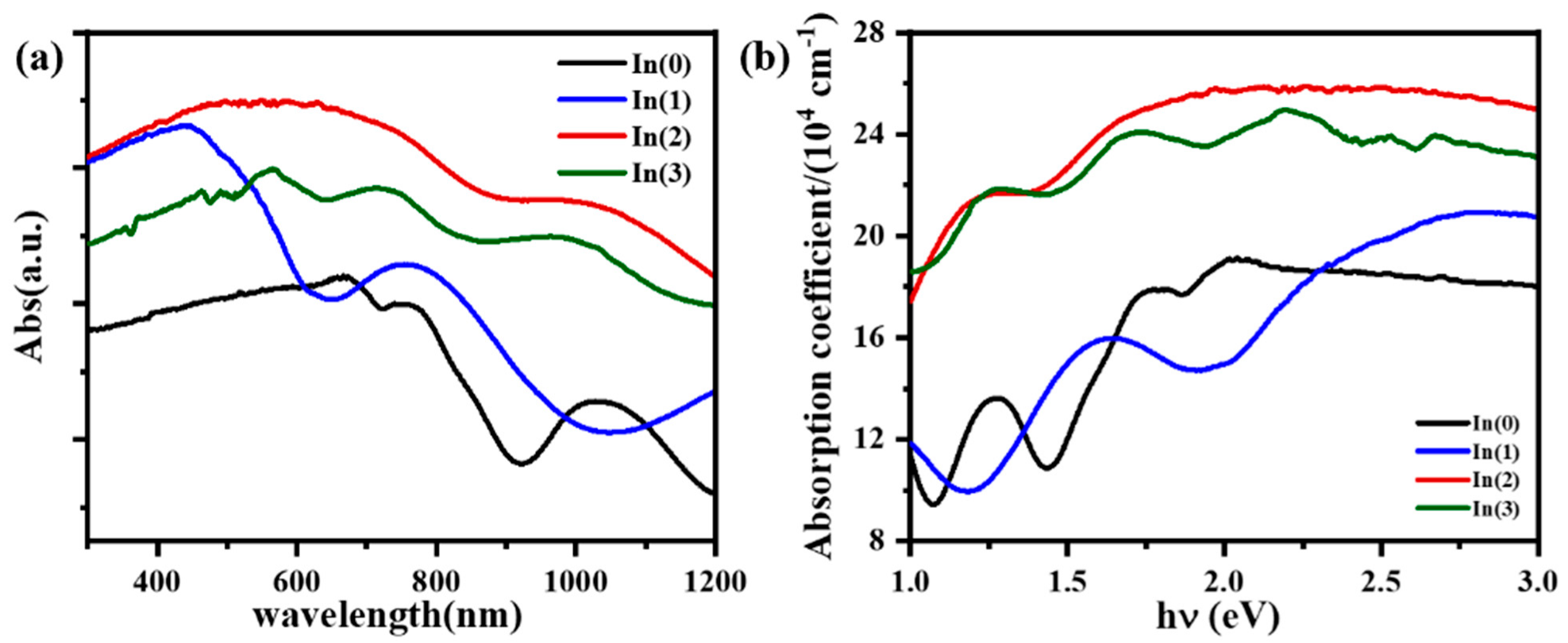
Figure 5a shows the UV-Vis-NIR diffuse reflectance absorption spectra of the different samples. Compared to the undoped SnS film, the light absorption performance of the In(1) sample shows a slight enhancement. As the doping concentration increases, the In(2) sample exhibits a significant enhancement in light absorption. However, when the doping concentration is further increased to a higher level, the light absorption intensity of the In(3) sample shows a decreasing trend.
More importantly, the absorption edge in Figure 5a shifts progressively toward longer wavelengths with increasing In content, suggesting a narrowing of the optical band gap.
The optical absorption coefficients of the different samples were calculated according to Equations (8) and (9) [32,33], and the resulting absorption coefficient curves are shown in Figure 5b:
T = 10 A
α = 1 d ln 1 T
where T is the transmittance of the material, A is the absorbance, α is the optical absorption coefficient, and d is the film thickness.
The measured thicknesses of the In(0), In(1), In(2), and In(3) films, which were all deposited for 20 min at a power of 80 W, were 462 nm, 460 nm, 454 nm, and 455 nm, respectively. The absorption coefficient of the In(1) sample is not significantly different from that of the undoped sample, indicating that a lower doping concentration has a limited effect on improving the film’s light absorption performance. In contrast, the In(2) and In(3) samples exhibit a marked increase in absorption coefficients. Notably, the In(2) sample reaches a maximum value of approximately 2.5 × 105 cm−1, about 1.5 times higher than the undoped film (1.7 × 105 cm−1). This indicates enhanced photon absorption capacity induced by moderate In doping.
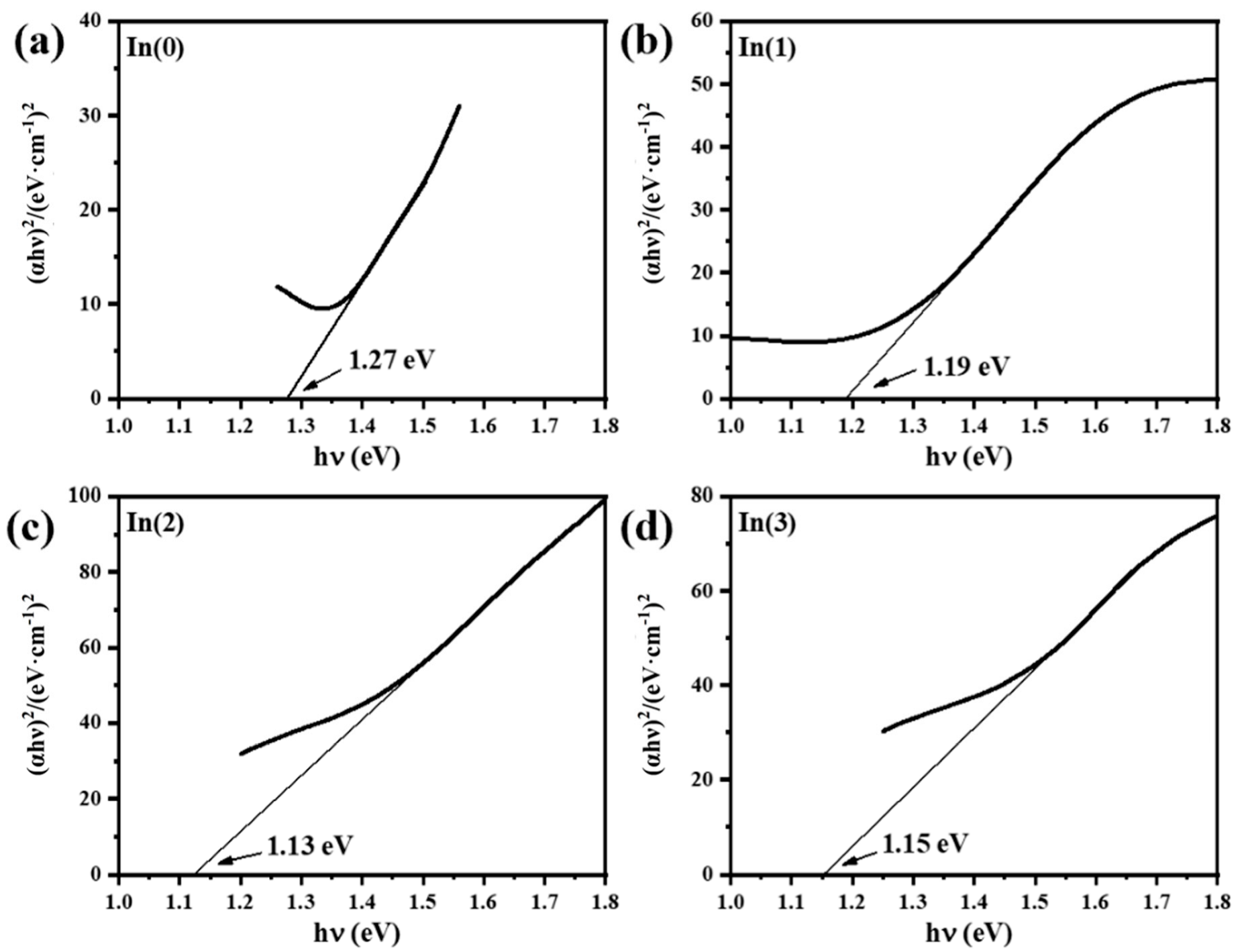
The band gap of the films was calculated using the Tauc equation [34,35]. By plotting the (αhν)2 vs. hν curves and using linear extrapolation, the direct band gap of each sample was estimated, with the results shown in Figure 6. The undoped SnS has a band gap of 1.27 eV. With the introduction of In3+ ions, the band gap of the In(1) sample at a lower doping concentration is reduced to 1.19 eV. As the doping concentration is further increased, the band gap of the In(2) sample decreases to a minimum value of 1.13 eV. This band edge shift is inferred from optical measurements and is consistent with previous studies, although further confirmation through band structure calculations or UPS/XPS analysis is needed. This reduction in band gap allows the material to absorb a broader range of the solar spectrum, especially in the visible to near-infrared region (420–1100 nm), thereby enhancing its light-harvesting capability and promoting higher photocurrent generation. Such enhancement is critical for improving the performance of optoelectronic devices, particularly in solar energy conversion and photodetection. However, when the doping concentration is increased further, the band gap of the In(3) sample slightly increases to 1.15 eV. The reduction in the band gap is primarily attributed to two key mechanisms: on one hand, the increase in carrier concentration causes a band shrinkage effect, leading to a smaller band gap; on the other hand, the substitution of Sn2+ by In3+ in the SnS lattice introduces additional impurity energy levels near the conduction band edge, which alters the material’s band structure and ultimately lowers the direct band gap energy. When the doping concentration is too high, the increase in the band gap can be attributed to excessive lattice distortion caused by the surplus of dopant ions. This generates significant stress within the material, damages the crystal structure, and leads to band gap widening, which adversely affects the film’s light absorption properties [9,13]. These findings highlight the effectiveness of In doping in modulating the band gap and are comparable to other studies on SnS doping, such as research on Cd doping, which reported a band gap reduction to 1.40 eV with 1.5% Cd-doping [36].

3.1.5. Photoelectric Performance Characterization

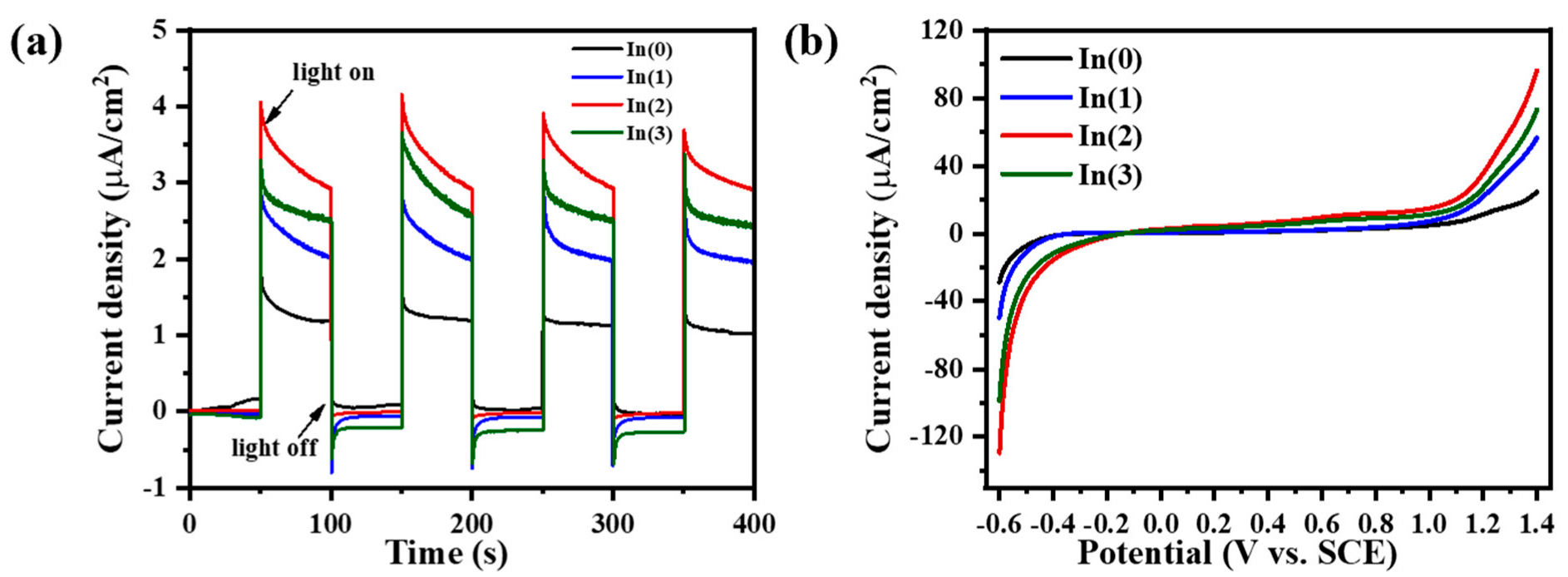
Photocurrent measurements of the various samples were conducted under visible light. Figure 7a shows the current-time curves at open-circuit potential, and Figure 7b displays the current as a function of applied voltage. With the increase in In3+ doping concentration, the photocurrent density of the SnS films exhibits a trend of first increasing and then decreasing. When the doping concentration reaches 4.93% (the In(2) sample), the film’s photocurrent density reaches a maximum value of 2.91 µA/cm2, which is 2.3 times that of the undoped sample. However, when the doping concentration is further increased to 6.06% (the In(3) sample), the photocurrent density decreases to 2.62 µA/cm2. This maximum photocurrent density is higher than the 2.53 µA/cm2 reported for Pb-doped SnS nanostructures [37], highlighting the effectiveness of In doping in enhancing the photoresponse of SnS films.
The electrical properties of the samples were tested using the Hall effect, with the results shown in Table 4. All In-doped SnS films were found to be of n-type conductivity. The In doping concentration has a significant impact on the film’s electrical properties. Within a moderate doping range (the In(1) and In(2) samples), both the carrier concentration and mobility of the films increase with the doping concentration. Among them, the In(2) sample exhibits the most excellent electrical properties, with a carrier concentration of 1.08 × 1016 cm−3 and a mobility of 1.48 cm2/Vs, showing a significant improvement over the undoped sample. For the In(3) sample with a further increased doping concentration, the carrier concentration and mobility begin to decrease. This trend is also reflected in the film’s resistivity. As the doping concentration increases from 0% to 4.93%, the resistivity decreases from 1.360 × 10⁴ Ω·cm to 5.67 × 10³ Ω·cm. When the doping concentration is further increased, the resistivity rises back to 6.70 × 10³ Ω·cm. This trend of decreasing resistivity with optimal doping is consistent with other studies on SnS films. For instance, research on Cd doping showed that a resistivity of 1.3 × 10⁴ Ω⋅cm was achieved at a 1.5% Cd doping level [36], indicating that both In and Cd can effectively reduce the resistivity of SnS films.
The decrease in resistivity is primarily attributed to the successful substitution of Sn2+ sites in the SnS lattice by In3+ ions. This substitutional doping provides more free electrons and creates an effective charge compensation effect, thereby significantly increasing the material’s carrier concentration [37,38]. Simultaneously, In-doping reduces the band gap and improves the light absorption capability of the SnS film, leading to a significant enhancement in photocurrent density under visible light illumination. When the doping concentration exceeds the optimal range, the decline in electrical properties may be due to the co-existence of substitutional and interstitial doping, which damages the integrity of the crystal structure. An excessively high doping concentration can introduce significant internal stress in the lattice, which exacerbates phonon scattering and ionized impurity scattering effects, adversely affecting the charge carrier transport efficiency [39,40].
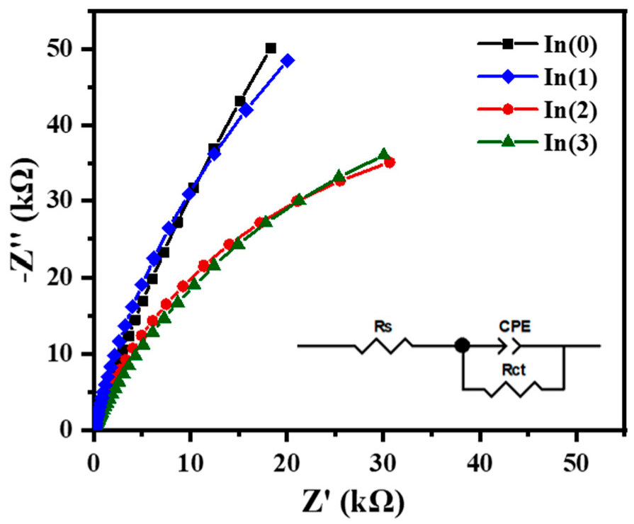
Electrochemical impedance spectroscopy (EIS) tests were conducted on the In-doped SnS thin films, and the Nyquist plots are shown in Figure 8. The EIS spectra of all samples exhibit a semicircular shape, indicating that the electrochemical process at the semiconductor/electrolyte interface is primarily controlled by charge transfer. The data were fitted using the equivalent circuit shown in the Figure, and the fitted parameters are listed in Table 5. As the doping concentration increases, the charge transfer resistance (Rct) of the samples first rapidly decreases from 559.99 kΩ to 99.64 kΩ, and then slightly increases to 126.16 kΩ. The electron transfer rate constant (k0) [41] and the exchange current density (J0) [42] at the film/electrolyte interface were calculated using Equations (10) and (11):
k 0 = R T n 2 F 2 A R c t C
J 0 = R T n F R c t
k0 and J0 represent the electron transfer rate constant and the exchange current density, respectively. R is the ideal gas constant (8.314 J·mol−1·K−1), T is the absolute temperature (K), F is the Faraday constant (96485 C·mol−1), and n is the number of electrons transferred in the electrochemical reaction. Furthermore, A is the working area of the electrode, C is the concentration of the active species in the electrolyte, and Rct is the charge transfer resistance obtained by fitting the Nyquist plots from Electrochemical Impedance Spectroscopy (EIS).
The In(2) sample, with a doping concentration of 4.93%, exhibits the highest electron transfer rate constant (k0) and exchange current density (J0) of 1.314 × 10⁻⁸ m/s and 1.268 × 10⁻⁷ A/cm2, respectively, which are 5.6 times higher than those of the undoped sample. Therefore, the In-doped SnS films have a higher charge transfer capability than the undoped film. However, doping beyond the optimal concentration hinders the charge carrier transport process [43].

3.2. Construction and Performance Enhancement of SnS-In/TiO2 Heterojunctions

3.2.1. Film Thickness and Crystal Structure Analysis

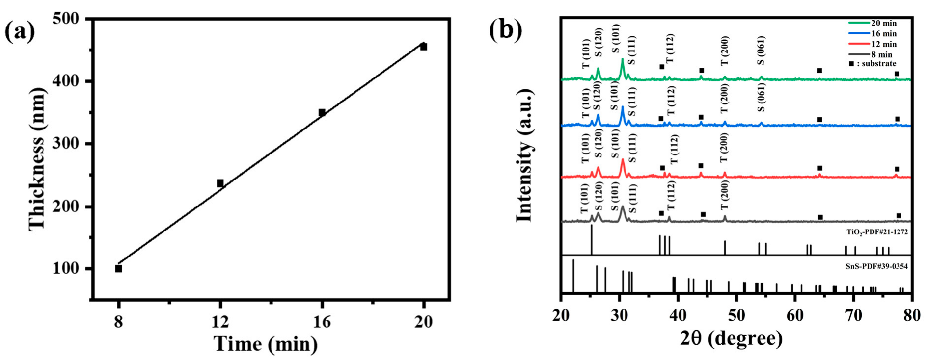
Since the deposition rate of the SnS-In film is stable, SnS-In/TiO2 heterostructures with different SnS-In layer thicknesses were prepared by varying the sputtering time of the SnS-In layer. The thicknesses of the SnS-In and TiO2 layers for each sample are shown in Table 6. The sputtering power of the SnS-In target was held constant at 80 W, and the thickness of the SnS-In layer increased linearly with time, as shown in Figure 9a. The fitted R2 value of 0.9942 indicates a good linear relationship between the film thickness and sputtering time. As the deposition time was extended from 8 min to 20 min, the thickness of the SnS-In layer increased from 100 nm to 455 nm. Meanwhile, the thickness of the TiO2 layer remained essentially unchanged.
Figure 9b shows the XRD patterns of the SnS-In/TiO2 bilayer films. Diffraction peaks for both SnS and TiO2 crystals are present in all samples. As the sputtering time is extended, the intensity of the TiO2 peaks gradually weakens, while the intensity of the SnS peaks progressively increases and their full width at half maximum (FWHM) narrows. This indicates that the crystallinity of the SnS-In layer improves with increasing film thickness. The diffraction peaks of the SnS-In layer correspond well with the standard diffraction card JCPDS No. 39-0354, indicating an orthorhombic polycrystalline structure. Diffraction peaks belonging to the (120), (101), and (111) planes appeared at approximately 26.35°, 30.53°, and 31.61°. For the samples sputtered for 16 min and 20 min, a diffraction peak for the (061) plane also appeared at 54.24°. Additionally, three diffraction peaks belonging to TiO2 can be observed, which match the standard diffraction card JCPDS No. 21-1272, confirming that the TiO2 is in the anatase phase. The peaks at 25.30°, 38.52°, and 48.00° correspond to the (101), (112), and (200) planes, respectively.
The grain sizes and strains of both the SnS-In and TiO2 were calculated [24,25], and the lattice constants of both films were determined using the Bragg equation and the interplanar spacing formula [26,44]. The calculated structural parameters are listed in Table 7. The grain size of the TiO2 films ranges from 27.0 to 27.5 nm, and their lattice constants are in good agreement with the standard values (3.7852 Å × 3.7852 Å × 9.5139 Å).
For the SnS-In layer, as the sputtering time increases from 8 min to 16 min, the grain size increases from 15.6 nm to 20.0 nm, while the strain decreases from 1.01 × 10⁻² to 7.78 × 10⁻³. This is due to the promoting effect of increased film thickness on the crystallization process. When the sputtering time is further extended to 20 min, the extent of grain growth becomes significantly smaller, indicating that the improvement in crystalline quality from increasing film thickness begins to be limited at this point.
For the SnS film, the lattice distortion caused by In-doping disrupts the crystal structure, leading to a reduction in grain size. When deposited on the TiO2 film, the grain size is further reduced due to the morphological fluctuations of the substrate surface and the lattice constant mismatch [33]. Consequently, the deviation from the standard lattice constants of SnS crystals (a = 4.3291 Å, b = 11.1923 Å, c = 3.9838 Å) is also further increased.

3.2.2. Surface Morphology Analysis

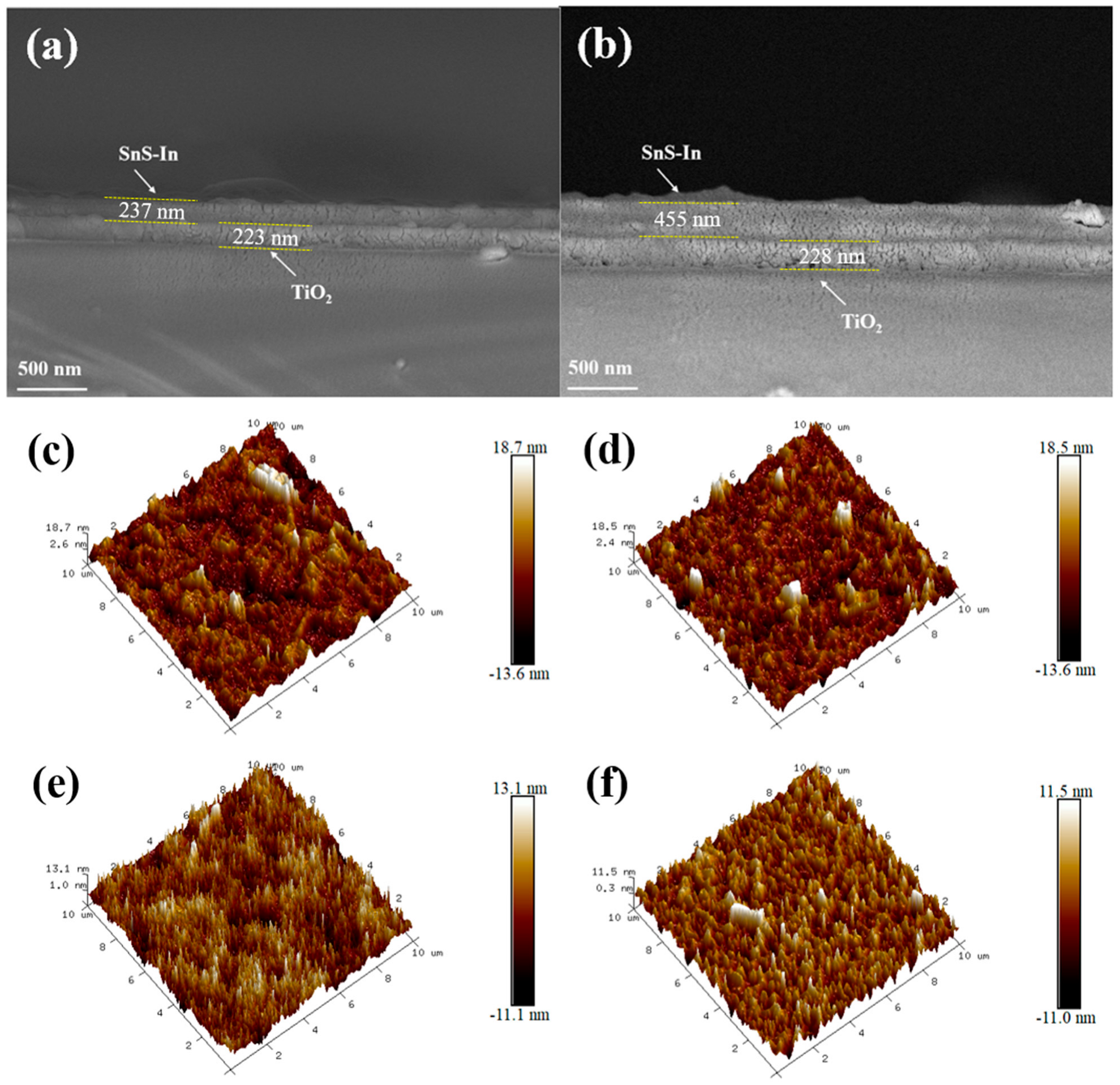
The morphological characterization of the heterojunction is shown in Figure 10. Figure 10a,b are the SEM cross-sectional images of the samples with SnS-In layer sputtering times of 12 min and 20 min. In Figure 10a, the thicknesses of the SnS-In and TiO2 layers are roughly equivalent. In Figure 10b, however, as the sputtering time increases, the thickness of the SnS-In layer gradually increases, reaching approximately twice that of the TiO2 layer.
Figure 10c–f show the AFM images of the various samples. When the sputtering time is shorter, resulting in a thinner SnS-In layer, the sample surface exhibits significant fluctuations and a higher defect density. As the sputtering time is extended, the film’s surface morphology gradually improves, with enhanced surface smoothness and more uniform particle distribution. The root-mean-square (RMS) surface roughness values for each sample are 3.91 nm, 3.54 nm, 3.36 nm, and 3.03 nm, respectively. The overall surface roughness of the SnS-In/TiO2 heterostructures is relatively large, but it gradually decreases as the thickness of the SnS-In layer increases.

3.2.3. Elemental Composition Analysis

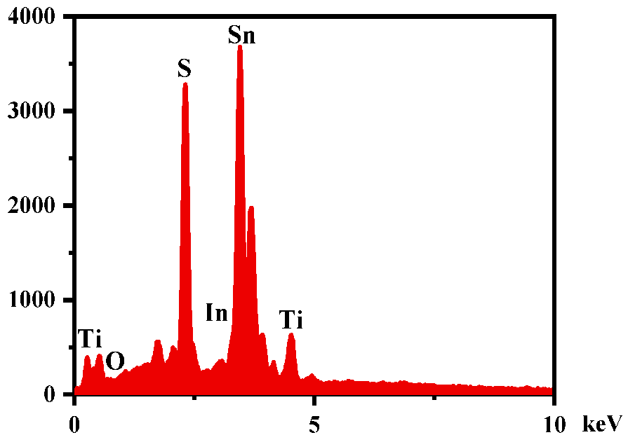
Figure 11 shows the EDS spectrum of the SnS-In/TiO2 heterostructure prepared with an 8 min sputtering time for the SnS-In layer, where the five characteristic elements—Sn, S, Ti, O, and In—were detected. The atomic percentages for the different samples are listed in Table 8. As the sputtering time increases, the atomic proportions of Sn, S, and In continually rise, while the atomic percentages of Ti and O decrease accordingly. In all samples, the atomic ratio of Ti to O is maintained in the range of 1:2.00 to 1:2.25, which is relatively close to the theoretical stoichiometry of TiO2. When four In pellets were embedded in the SnS target surface, the atomic ratio of Sn to In was 10.25. In this part of the experiment, the number of In pellets and the sputtering power were kept constant. In the heterostructures prepared by magnetron sputtering, the atomic ratio of Sn to In remained relatively close to 10.25. This result indicates that under fixed doping conditions, the sputtering process can effectively control the ratio of Sn to In, thereby ensuring the compositional stability of the In-doped SnS film.

3.2.4. Optical Absorption Characterization

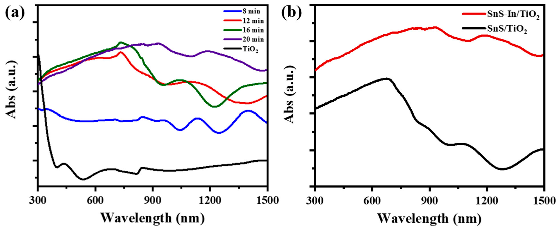
Figure 12a shows the UV-Vis-NIR diffuse reflectance spectra of the SnS-In/TiO2 heterostructures prepared with different sputtering times for the SnS-In layer. According to the preceding characterization results, the band gap of the SnS-In film, after optimization of the In doping concentration, can be reduced to 1.13 eV. Therefore, when it forms a heterojunction with wide-bandgap TiO2, the resulting structure exhibits a broadened spectral response range, showing particularly enhanced light absorption properties in the visible light region.
As the sputtering time increases from 8 to 20 min, the absorption intensity shows a clear upward trend across the full spectrum. The enhancement is especially prominent in the 600–1000 nm range, owing to the extended optical path and improved crystallinity.
However, when the sputtering time exceeds 12 min, the rate of absorption enhancement slows down significantly. In the initial stage of increasing film thickness, the light absorption efficiency is significantly improved due to the extended optical path length and the growth of grain size. When the film thickness increases to a certain extent, the light absorption efficiency gradually approaches saturation due to the exacerbation of light scattering effects and interfacial reflection losses [26,45]. Figure 12b compares the light absorption curves of the SnS-In/TiO2 and SnS/TiO2 structures, where the sputtering time for the light-absorbing layer in both cases is 20 min. Since In-doping can modulate the band structure of SnS and cause band gap shrinkage, incorporating In3+ into the SnS layer of the heterostructure can further enhance the light absorption performance of the sample [46].

3.2.5. Photoelectric Performance Characterization

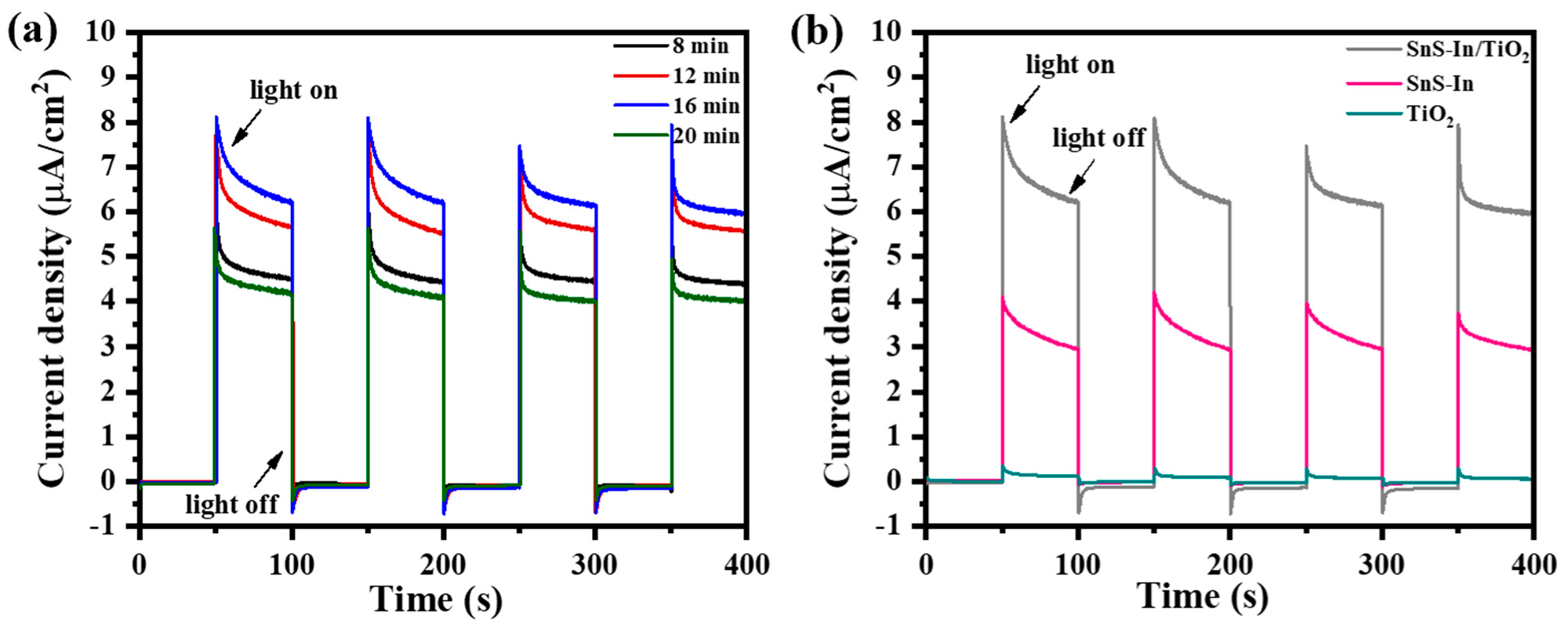
The photoelectric performance of the various samples was characterized under visible light using a three-electrode system, with the photocurrent test results shown in Figure 13. Figure 13a shows the current-time curves of the SnS-In/TiO2 heterostructures prepared with different sputtering times for the SnS-In layer. As the sputtering time increases from 8 min to 16 min, the photocurrent density of the films significantly increases from 4.52 µA/cm2 to 6.36 µA/cm2. This is likely due to the improvement in crystalline quality resulting from the increased film thickness, which in turn enhances the light absorption efficiency [47].
When the sputtering time is extended to 20 min, the photocurrent density of the film drops significantly to 4.40 µA/cm2, the lowest among all the heterostructure samples. This phenomenon is primarily attributed to the enhanced scattering of charge carriers at grain boundaries and interfaces when the film thickness exceeds the optimal range, leading to a decrease in transport efficiency and, thus, suppressing the charge transport performance [45]. Furthermore, due to the inherently low carrier mobility, a thicker film prevents some charge carriers from effectively reaching the electrode, which increases the probability of electron-hole recombination and further weakens the device’s photoresponsive capability.
Figure 13b compares the photocurrent of the heterostructure and single-layer films. The sputtering time for the SnS-In layer in the heterostructure was 16 min, and single-layer SnS-In and TiO2 films of equivalent thickness were prepared as controls. The photocurrent generated by the heterostructure under visible light is significantly higher than that of the single-layer films, being 2.2 times higher than the SnS-In film and 53.0 times higher than the TiO2 film.
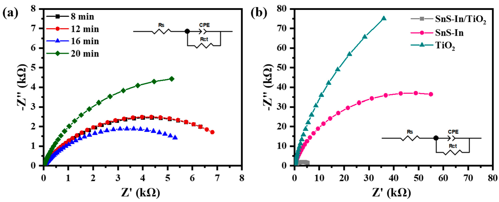
Figure 14 shows the results of the Electrochemical Impedance Spectroscopy (EIS) tests for the various samples. The EIS curves for all samples exhibit a semicircular feature, indicating that the electrochemical reaction kinetics at the semiconductor/electrolyte interface are predominantly governed by the charge transfer process [41]. The data were fitted using the equivalent circuit shown in the Figure, and the resulting parameters, along with the calculated electron transfer rate constant (k0) and exchange current density (J0) are listed in Table 9.
Compared to the single-layer SnS-In and TiO2 films, the charge transfer resistance (Rct) for all the heterostructure films is significantly reduced, indicating that this structure plays an important role in promoting charge carrier transport [41]. Correspondingly, compared to the single-layer films, both the electron transfer rate constant (k0) and the exchange current density (J0) at the heterostructure interface are one to two orders of magnitude higher. For the heterostructure films with different SnS-In layer thicknesses, as the sputtering time is extended from 8 min to 16 min, the sample’s charge transfer resistance (Rct) gradually decreases, reaching a minimum of 6.83 kΩ, while the electron transfer rate constant (k0) and exchange current density (J0) increase to 1.916 × 10⁻⁷ m/s and 1.848 × 10⁻⁶ A/cm2, respectively. However, when the thickness of the SnS-In layer is further increased (sputtering time of 20 min), the sample’s charge transfer resistance (Rct) rises again to 11.93 kΩ, and the charge transfer efficiency decreases once more.
Our previous work indicated that the SnS/TiO2 heterostructure exhibited optimal photoelectric performance when the SnS sputtering time was 12 min (thickness of approx. 244 nm) [21]. Based on this, we compared the performance of the sample prepared with the same sputtering time in the current study with that of the previous optimal sample, with the results shown in Figure 15. Under comparable absorption layer thicknesses, introducing In-doping into the absorption layer significantly enhances the photocurrent density of the heterostructure under visible light, while simultaneously reducing the interfacial charge transfer resistance and promoting the separation of charge carriers by the heterojunction. For the SnS-In/TiO2 heterostructure, the photoelectric performance is further enhanced when the sputtering time is 16 min, meaning that after In-doping, the optimal thickness of the SnS absorption layer increases to 350 nm. On one hand, this is because In-doping significantly improves the light absorption performance of the SnS film, which means the SnS-In/TiO2 heterostructure can utilize incident light more effectively. Therefore, the SnS-In layer requires a greater thickness to fully absorb photons and generate more photogenerated charge carriers [48]. On the other hand, In-doping optimizes the carrier mobility of the SnS layer, allowing it to maintain high carrier transport efficiency even at greater thicknesses without significantly increasing recombination losses [49,50].
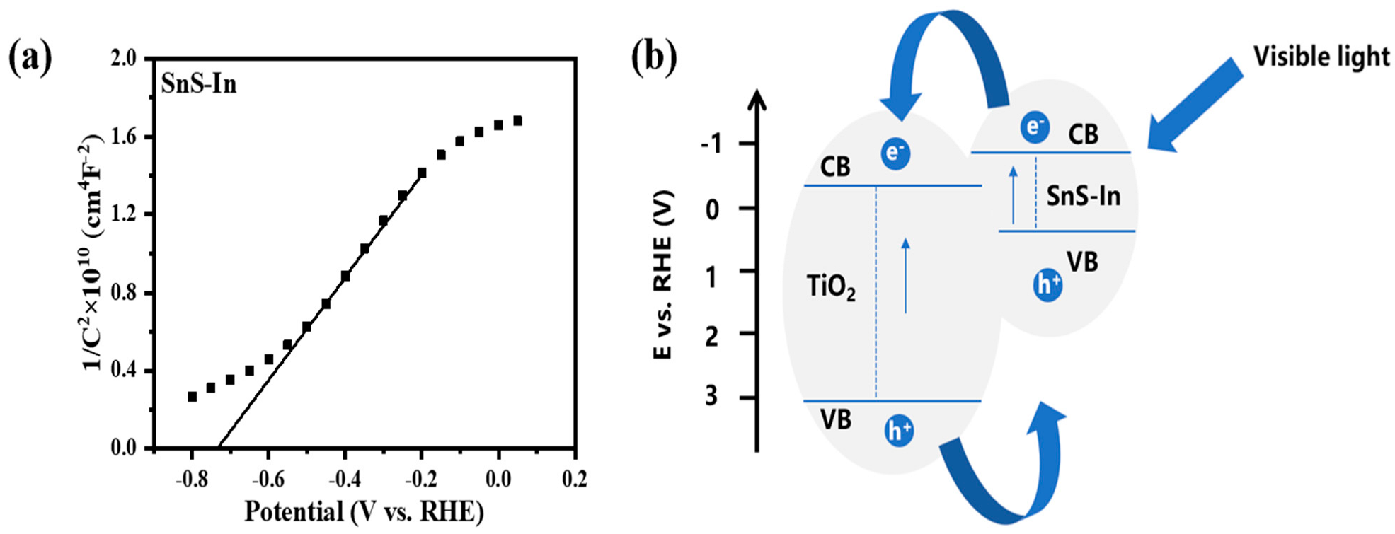
A Mott–Schottky (M-S) test was performed on the sample with an In doping concentration of 4.93%, and the resulting curve is shown in Figure 16a. By extrapolating the linear portion of the curve to the x-axis intercept, the flat-band potential (Vfb) of the sample can be obtained. From this, the flat-band potential of the In-doped SnS film was determined to be −0.73 V. For an n-type semiconductor, the conduction band potential (ECB) can be approximated as the flat-band potential (Vfb) [51]. Combined with the band gap width obtained from UV-Vis-NIR spectroscopy, the valence band potential (EVB) of the In-doped SnS film was calculated to be 0.40 V using Equations (5) and (6) [52]. Combining this with the previously determined band positions of the TiO2 film, a band structure diagram for the SnS-In/TiO2 heterostructure was constructed, as shown in Figure 16b. Compared to the undoped SnS film, In-doping causes the conduction band potential of the film to shift to a more negative direction, which may have a certain impact on the transfer of electrons to TiO2. However, according to the final photoelectric performance test results, In-doping significantly increases the carrier concentration and conductivity of SnS, which is sufficient to offset the negative effects brought about by the change in the conduction band position.
4. Discussion

This study aimed to systematically optimize the photoelectric properties of tin sulfide (SnS) thin films through Indium (In) doping and the construction of SnS-In/TiO2 heterojunctions. Our findings not only confirmed the significant modulating effect of In doping on the physicochemical characteristics of SnS but, more importantly, demonstrated a synergistic effect between In doping and heterostructure design that substantially enhances photoelectric conversion efficiency.
Firstly, structural analyses (XRD, AFM, Raman, and XPS) of the In-doped SnS thin films clearly indicated that In3+ ions successfully substituted Sn2+ sites in the SnS lattice, consistent with existing literature on In as a substitutional dopant in SnS. The smaller ionic radius of In3+ compared to Sn2+ led to a reduction in unit cell volume, accompanied by decreased grain size and increased lattice strain. Although In doping introduced some lattice defects and affected crystallinity to a certain extent, no new impurity phases were formed within the detectable range, laying a structural foundation for subsequent performance optimization. The observed increase in surface roughness directly reflects the grain refinement and enhanced irregularity in crystallization, which may be linked to the lattice stress induced by doping that restricts two-dimensional grain growth and promotes three-dimensional island nucleation.
The observed improvements in optical and electrical properties serve as direct evidence of successful In doping. SnS thin films with an optimal doping concentration (4.93 at%) exhibited a narrower band gap (reduced from 1.27 eV to 1.13 eV) and significantly enhanced light absorption capabilities. This band gap reduction primarily stems from two key mechanisms: increased carrier concentration leading to band shrinkage effects, and the formation of additional impurity energy levels near the conduction band edge due to In3+ substituting Sn2+ in the SnS lattice, which alters the material’s band structure and ultimately lowers the direct band gap energy. These findings align with related studies. Simultaneously, as a donor impurity, In doping effectively increased the carrier concentration and mobility of SnS, thereby significantly lowering its resistivity and transforming the film from a semiconductor to a more optimally n-type conductive material. Photocurrent measurements and EIS results further confirmed that appropriate In doping can effectively boost the photocurrent density and charge transfer efficiency, which is intrinsically linked to the improved light absorption and carrier transport properties imparted by In doping. However, when the doping concentration exceeded the optimal range, excessive doping ions exacerbated lattice distortion, increasing phonon scattering and ionized impurity scattering effects, which in turn inhibited carrier transport efficiency and led to band gap widening, ultimately causing a decline in photoelectric performance. This underscores the critical importance of finding an optimal balance in doping engineering.
Building upon the optimized performance of single-layer films, we further constructed SnS-In/TiO2 heterojunctions, aiming to leverage interfacial effects to promote photogenerated charge separation and transport. The results revealed that compared to single-layer SnS-In and TiO2 thin films, the photoelectric performance of the SnS-In/TiO2 heterojunction was enhanced by orders of magnitude, with a peak photocurrent density of 6.36 µA/cm2. This remarkable improvement is primarily attributed to two synergistic mechanisms. Firstly, In doping optimized the band gap and electrical properties of SnS, making it a more efficient visible light absorber and charge generation layer. Secondly, the formation of a Type-II heterojunction between SnS-In and wide-bandgap n-type TiO2 created a favorable band alignment that facilitated the transfer of photogenerated electrons from the conduction band of SnS-In to that of TiO2, while holes transferred from the valence band of TiO2 to that of SnS-In. This effectively suppressed electron-hole recombination and significantly enhanced charge separation and transport rates. The significant reduction in charge transfer resistance (Rct) and the substantial increase in electron transfer rate constant (k0) and exchange current density (J0) observed in the EIS results strongly support the role of the heterojunction interface in promoting efficient charge separation and transport.
Notably, we observed a change in the optimal thickness of the SnS-In layer within the heterojunction. Our previous work indicated that for pure SnS/TiO2 heterojunctions, the optimal SnS layer thickness was approximately 244 nm (12 min sputtering time). However, in the current study, the In-doped SnS-In/TiO2 heterojunction exhibited optimal photoelectric performance when the SnS-In layer thickness was 350 nm (16 min sputtering time). This suggests that In doping not only enhanced the light absorption capability of the SnS thin film, necessitating a thicker layer for fuller light utilization, but also optimized the carrier mobility of the SnS layer. This optimization allowed for sustained high carrier transport efficiency even with increased thickness, effectively mitigating recombination losses that might otherwise occur with thicker films. When the film thickness exceeded the optimal range, the photoelectric performance declined, likely due to enhanced carrier scattering at grain boundaries and interfaces, as well as an increased probability of electron-hole recombination as some carriers failed to efficiently reach the electrode.
This work confirms the effectiveness of combining In doping for SnS band engineering with TiO2 heterostructure construction, providing a novel strategy for developing high-performance optoelectronic conversion materials. Although the reported photoelectric performance is moderate, it serves as a solid foundation for subsequent device optimization.
Future research can further explore more refined In doping profiles or alternative doping strategies (e.g., co-doping or gradient doping) to fine-tune carrier concentration and mobility. In addition, optimizing the microstructure and chemical quality of the SnS-In/TiO2 interface—through interfacial passivation, insertion of buffer layers, or energy level alignment engineering—could significantly reduce interfacial recombination and enhance charge transport. Improvements in film crystallinity, surface morphology, and electrode configuration (e.g., transparent or grid-based electrodes) are also expected to contribute to better light absorption and carrier extraction. These efforts will help push the device performance beyond the current level and expand its potential applications in fields such as photocatalytic water splitting, photodetectors, and next-generation thin-film solar cells.

5. Conclusions

This study systematically investigated the synergistic enhancement effect of In-doping and heterostructure construction on the photoelectric properties of SnS thin films. First, In-doped SnS films were successfully prepared by co-sputtering, and it was found that the In doping concentration is a key factor in modulating their microstructure and photoelectric properties. Due to the substitution of Sn2+ by In3+, an optimal In doping level (4.93 at.%) effectively optimized the band structure of SnS (reducing the band gap to 1.13 eV) and significantly enhanced the carrier concentration (1.08 × 1016 cm−3) and mobility (1.48 cm2/Vs), which in turn increased the film’s photocurrent response from 1.27 µA/cm2 (undoped) to 2.91 µA/cm2. However, excessive doping exacerbates lattice distortion and, conversely, inhibits charge carrier transport.
Second, the SnS-In/TiO2 heterojunction, constructed based on the optimally doped component, further magnified the advantages in photoelectric performance. By optimizing the thickness of the SnS-In layer to 350 nm, the interfacial charge transfer efficiency of the heterojunction was maximized. Ultimately, the SnS-In/TiO2 device achieved a photocurrent density of 6.36 µA/cm2, far surpassing that of the single-layer SnS-In film (2.91 µA/cm2) and the optimal SnS/TiO2 heterostructure (with a 244 nm thick SnS layer).

Author Contributions

Conceptualization, J.L. and J.S.; methodology, J.L.; validation, Y.D., J.L. and M.Z.; formal analysis, Y.D. and J.L.; investigation, Y.D., J.L. and M.Z.; writing—original draft preparation, J.L. and J.S.; writing—review and editing, J.L. and J.S.; supervision, J.S.; project administration, J.S.; funding acquisition, J.S. All authors have read and agreed to the published version of the manuscript.

Funding

This work was supported by the Natural Science Foundation of China (No. 61671155).

Data Availability Statement

The original contributions presented in this study are included in the article. Further inquiries can be directed to the corresponding author.

Acknowledgments

The authors express gratitude to the Department of Materials Science in Fudan University for the magnetron sputtering equipment. Additionally, special thanks are extended to Xiaoli Cui for her guidance and assistance during the photoelectric characterization.

Conflicts of Interest

The authors declare no conflicts of interest.

References

  1. Patel, M.; Yu, X.; Kim, Y.K.; Kim, J. Facile formation of nanodisk-shaped orthorhombic SnS layers from SnS2 particles for photoelectrocatalytic hydrogen production. ChemNanoMat 2017, 3, 591–600. [Google Scholar] [CrossRef]
  2. Tang, R.; Su, H.; Sun, Y.; Zhang, X.; Li, L.; Liu, C.; Zeng, S.; Sun, D. Enhanced photocatalytic performance in Bi2WO6/SnS heterostructures: Facile synthesis, influencing factors and mechanism of the photocatalytic process. J. Colloid Interface Sci. 2016, 466, 388–399. [Google Scholar] [CrossRef] [PubMed]
  3. Zheng, X.; De Luna, P.; García de Arquer, F.P.; Zhang, B.; Becknell, N.; Ross, M.B.; Li, Y.; Banis, M.N.; Li, Y.; Liu, M.; et al. Sulfur-modulated tin sites enable highly selective electrochemical reduction of CO2 to formate. Joule 2017, 1, 794–805. [Google Scholar] [CrossRef]
  4. Li, F.; Moayed, M.M.R.; Gerdes, F.; Kull, S.; Klein, E.; Lesyuk, R.; Klinke, C. Colloidal tin sulfide nanosheets: Formation mechanism, ligand-mediated shape tuning and photo-detection. J. Mater. Chem. C 2018, 6, 9410–9419. [Google Scholar] [CrossRef]
  5. Jamali-Sheini, F.; Cheraghizade, M.; Yousefi, R. SnS nanosheet films deposited via thermal evaporation: The effects of buffer layers on photovoltaic performance. Sol. Energy Mater. Sol. Cells 2016, 154, 49–56. [Google Scholar] [CrossRef]
  6. Han, J.; Yin, X.; Nan, H.; Zhou, Y.; Yao, Z.; Li, J.; Oron, D.; Lin, H. Enhancing the performance of perovskite solar cells by hybridizing SnS quantum dots with CH3NH3PbI3. Small 2017, 13, 1700953. [Google Scholar] [CrossRef]
  7. Suzuki, I. Carrier control in SnS by doping: A review. J. Ceram. Soc. Jpn. 2023, 131, 777–788. [Google Scholar] [CrossRef]
  8. Behera, C.; Ghosh, S.P.; Kar, J.P.; Samal, S.L. Facile synthesis and enhanced photocatalytic activity of Ag-SnS nanocomposites. New J. Chem. 2020, 44, 11684–11693. [Google Scholar] [CrossRef]
  9. Bommireddy, P.R.; Musalikunta, C.S.; Uppala, C.; Park, S.H. Influence of Cu doping on physical properties of sol-gel processed SnS thin films. Mater. Sci. Semicond. Process. 2017, 71, 139–144. [Google Scholar] [CrossRef]
  10. Qin, Y.X.; Qiu, P.L.; Bai, Y.N. First-principles calculations combined with experiments to study the gas-sensing performance of Zn-substituted SnS. Phys. Chem. Chem. Phys. 2020, 22, 17513–17522. [Google Scholar] [CrossRef]
  11. Hsu, H.T.; Chiang, M.H.; Huang, C.H.; Lin, W.T.; Fu, Y.S.; Guo, T.F. Effects of Ge- and Sb-doping and annealing on the tunable bandgaps of SnS films. Thin Solid Films 2015, 584, 37–40. [Google Scholar] [CrossRef]
  12. Chaki, S.H.; Chaudhary, M.D.; Deshpande, M.P. Effect of indium and antimony doping in SnS single crystals. Mater. Res. Bull. 2015, 63, 173–180. [Google Scholar] [CrossRef]
  13. Dussan, A.; Mesa, F.; Gordillo, G. Effect of substitution of Sn for Bi on structural and electrical transport properties of SnS thin films. J. Mater. Sci. 2010, 45, 2403–2407. [Google Scholar] [CrossRef]
  14. Qiu, P.; Qin, Y.; Bai, Y.; Xia, Q.; Zheng, A. Gas selectivity regulation of monolayer SnS by introducing nonmetallic dopants: A combined theoretical and experimental investigation. Appl. Surf. Sci. 2021, 570, 151155. [Google Scholar] [CrossRef]
  15. Kawanishi, S.; Suzuki, I.; Ohsawa, T.; Ohashi, N.; Shibata, H.; Omata, T. Growth of large single crystals of n-type SnS from halogen-added Sn flux. Cryst. Growth Des. 2020, 20, 5931–5939. [Google Scholar] [CrossRef]
  16. Iguchi, Y.; Sato, K.; Inoue, K.; Fukui, K.; Yanagi, H. Br-doped n-type SnS single crystals with carrier concentrations suitable for homojunction solar cells. Solid State Sci. 2023, 140, 107206. [Google Scholar] [CrossRef]
  17. Lim, S.Y.; Brahma, S.; Liu, C.P.; Wang, R.C.; Huang, J.L. Effect of indium concentration on luminescence and electrical properties of indium doped ZnO nanowires. Thin Solid Film. 2013, 549, 165–171. [Google Scholar] [CrossRef]
  18. Abd El-Hady, S.A.; Ibrahim, A.M.; Rammah, Y.S. Structural, optical and electrical properties of In-doped SnS thin films prepared by spray pyrolysis technique for optoelectronic applications. Phys. B Condens. Matter 2021, 600, 412586. [Google Scholar]
  19. Khan, M.I.; Bhatti, K.A.; Qayyum, A. Structural, optical and electrical properties of indium doped tin sulfide thin films prepared by chemical bath deposition method. J. Alloys Compd. 2016, 680, 16–21. [Google Scholar]
  20. Wei, J.; Wang, Y.; Zhu, C. Enhanced Photoelectric Performance of SnS-Based Photodetector via Indium Doping and Piezo-phototronic Effect. Adv. Electron. Mater. 2022, 8, 2200371. [Google Scholar]
  21. Ding, Y.; Leng, J.; Zhang, M.; Shen, J. Photoelectric and Photocatalytic Properties of SnS/TiO2 Heterostructure Thin Films Prepared by Magnetron Sputtering Method. Inorganics 2025, 13, 208. [Google Scholar] [CrossRef]
  22. Xu, F.; Scaramuzza, N.; Versace, C. Decorating TiO2 nanoparticle thin film with SnSx(x<1): Preparation, characterization, and photocatalytic activity. Coatings 2024, 14, 1185. [Google Scholar]
  23. Shah, P.; Modi, K.; Patel, R.P.; Pataniya, P.M.; Sathe, V.; Sumesh, C.K. Scalable and cost-effective synthesis of flexible paper-based Indium doped SnS photodetector in the VIS-NIR range. Surf. Interfaces 2023, 42, 103408. [Google Scholar] [CrossRef]
  24. Guneri, E.; Ulutas, C.; Kirmizigul, F.; Altindemir, G.; Gode, F.; Gumus, C. Effect of deposition time on structural, electrical, and optical properties of SnS thin films deposited by chemical bath deposition. Appl. Surf. Sci. 2010, 257, 1189–1195. [Google Scholar] [CrossRef]
  25. Hase, Y.; Sharma, V.; Doiphode, V.; Waghmare, A.; Punde, A.; Shinde, P.; Shah, S.; Rahane, S.; Vairale, P.; Bade, B.; et al. Humidity sensor properties of hydrothermally grown rutile-TiO2 microspheres on interdigital electrodes (IDEs). J. Mater. Sci. Mater. Electron. 2022, 33, 11825–11840. [Google Scholar] [CrossRef]
  26. Kul, M. Electrodeposited SnS film for photovoltaic applications. Vacuum 2014, 107, 213–218. [Google Scholar] [CrossRef]
  27. Reddy, N.K.; Devika, M.; Hahn, Y.B.; Gunasekhar, K.R. Impact of chemical treatment on the surface, structure, optical and electrical properties of SnS thin films. Appl. Surf. Sci. 2013, 268, 317–322. [Google Scholar] [CrossRef]
  28. Kafashan, H. Structural characterizations of pure SnS and In-doped SnS thin films using isotropic and anisotropic models. Mater. Res. Express 2018, 5, 046417. [Google Scholar] [CrossRef]
  29. Baby, B.H.; Philipson, A.; Mohan, D.B. Temperature-assisted mechanochemically synthesized Cu and In doped SnS nanoparticles for thin film photovoltaics: Structure, phase stability and optoelectronic properties. Optik 2021, 240, 166848. [Google Scholar] [CrossRef]
  30. Baby, B.H.; Mohan, D.B. The effect of in-situ and post deposition annealing towards the structural optimization studies of RF sputtered SnS and Sn2S3 thin films for solar cell application. Sol. Energy 2019, 189, 207–218. [Google Scholar] [CrossRef]
  31. Reddy, V.M.; Gedi, S.; Park, C.; R.W., M.; K.T., R.R. Development of sulphurized SnS thin film solar cells. Curr. Appl. Phys. 2015, 15, 588–598. [Google Scholar] [CrossRef]
  32. Banai, R.E.; Lee, H.; Motyka, M.A.; Chandrasekharan, R.; Podraza, N.J.; Brownson, J.R.S.; Horn, M.W. Optical properties of sputtered SnS thin films for photovoltaic absorbers. IEEE J. Photovoltaics 2013, 3, 1084–1089. [Google Scholar] [CrossRef]
  33. Bashkirov, S.A.; Gremenok, V.F.; Ivanov, V.A.; Shevtsova, V.V.; Gladyshev, P.P. Influence of substrate material on the microstructure and optical properties of hot wall deposited SnS thin films. Thin Solid Films 2015, 585, 40–44. [Google Scholar] [CrossRef]
  34. Tauc, J.; Grigorovici, R.; Vancu, A. Optical properties and electronic structure of amorphous germanium. Phys. Status Solidi B 1966, 15, 627–637. [Google Scholar] [CrossRef]
  35. Coulter, J.B.; Birnie, D.P. Assessing Tauc plot slope quantification: ZnO thin films as a model system. Phys. Status. Solidi B 2018, 255, 1700393. [Google Scholar] [CrossRef]
  36. Bano, S.; Khan, M.I.; Albalawi, H.; Islam, G.u.; Siddique, M.; Ahmad, T.; Alkhaldi, H.; farhat, l.b.; Ahson, R.; Hussain, S. Effect of Cd doping on the structural, optical, and photovoltaic properties of SnS films. J. Mater. Res. Technol. 2022, 19, 1982–1992. [Google Scholar] [CrossRef]
  37. Niknia, F.; Jamali-Sheini, F.; Yousefi, R. Photocurrent properties of undoped and Pb-doped SnS nanostructures grown using electrodeposition method. J. Electron. Mater. 2015, 44, 4734–4739. [Google Scholar] [CrossRef]
  38. Gedi, S.; Reddy, V.M.; Kotte, T.R.; Kim, S.H.; Jeon, C.W. Chemically synthesized Ag-doped SnS films for PV applications. Ceram. Int. 2016, 42, 19027–19035. [Google Scholar] [CrossRef]
  39. Jamali-Sheini, F.; Cheraghizade, M.; Yousefi, R. Ultrasonic synthesis of In-doped SnS nanoparticles and their physical properties. Solid State Sci. 2018, 79, 30–37. [Google Scholar] [CrossRef]
  40. Sebastian, S.; Kulandaisamy, I.; Arulanantham, A.M.S.; Valanarasu, S.; Kathalingam, A.; Jebathew, A.J.; Shkir, M.; Karunakaran, M. Influence of Al doping concentration on the opto-electronic chattels of SnS thin films readied by NSP. Opt. Quant. Electron. 2019, 51, 100. [Google Scholar] [CrossRef]
  41. Baby, B.H.; Thomas, A.M.; Amrutha, E.G.; Mohan, D.B. Enhancement of optoelectronic properties via substitutional doping of Cu, In and Ag in SnS nanorods for thin film photovoltaics. Sol. Energy 2020, 205, 446–455. [Google Scholar] [CrossRef]
  42. Mishra, S.K.; Kumar, D.; Biradar, A.M.; Rajesh, A. Electrochemical impedance spectroscopy characterization of mercaptopropionic acid capped ZnS nanocrystal based bioelectrode for the detection of the cardiac biomarker-myoglobin. Bioelectrochemistry 2012, 88, 118–126. [Google Scholar] [CrossRef] [PubMed]
  43. Li, P.; Zhang, Y.; Yang, X.; Gao, Y.; Ge, S. Alloyed PtNi counter electrodes for high-performance dye-sensitized solar cell applications. J. Alloys Compd. 2017, 725, 1272–1281. [Google Scholar] [CrossRef]
  44. Kafashan, H. Optoelectronic properties of In-doped SnS thin films. Ceram. Int. 2019, 45, 334–345. [Google Scholar] [CrossRef]
  45. Javed, A.; Khan, N.; Bashir, S.; Ahmad, M.; Bashir, M. Thickness dependent structural, electrical and optical properties of cubic SnS thin films. Mater. Chem. Phys. 2020, 246, 122831. [Google Scholar] [CrossRef]
  46. Selim, M.S.; Gouda, M.E.; El-Shaarawy, M.G.; Salem, A.M.; El-Ghany, W.A. Abd. Effect of thickness on optical properties of thermally evaporated SnS films. Thin Solid Films 2013, 527, 164–169. [Google Scholar] [CrossRef]
  47. Yu, X.; Xing, Q.; Zhang, X.; Jiang, H.; Cao, F. Photoelectric water splitting using TiO2 nanorod arrays coated with Zn-doped CdS. J. Mater Sci. 2021, 56, 11059–11070. [Google Scholar] [CrossRef]
  48. Huang, L.Y.; Meng, L. Effects of film thickness on microstructure and electrical properties of the pyrite films. Mater. Sci. Eng. B 2007, 137, 310–314. [Google Scholar] [CrossRef]
  49. Yu, L.; Li, Z.; Liu, Y.; Cheng, F.; Sun, S. Mn-doped CdS quantum dots sensitized hierarchical TiO2 flower-rod for solar cell application. Appl. Surf. Sci. 2014, 305, 359–365. [Google Scholar] [CrossRef]
  50. Tu, J.; Li, J.; Pan, Z.; Zhu, X.; Ye, D.; Yang, Y.; Wang, H.; An, L.; Chen, R.; Liao, Q. Nitrogen-doped CdS/TiO2 nanorods heterojunction photoanode for efficient and stable photoelectric water splitting. J. Power Sources 2025, 628, 235883. [Google Scholar] [CrossRef]
  51. Veerathangam, K.; Pandian, M.S.; Ramasamy, P. Incorporation of Co2+ in CdS quantum dots for solar cell applications. Mater. Sci. Semicond. Process. 2020, 108, 104869. [Google Scholar] [CrossRef]
  52. Ellis, A.B.; Kaiser, S.W.; Bolts, J.M.; Wrighton, M.S. Study of n-type semiconducting cadmium chalcogenide-based photoelectric cells employing polychalcogenide electrolytes. J. Am. Chem. Soc. 1977, 99, 2839–2848. [Google Scholar] [CrossRef]
Figure 1. In-doped SnS thin films: (a) XRD patterns; (b) Raman spectra.
Coatings 15 00972 g001
Figure 2. Texture Coefficient (TC) of In-Doped SnS Thin Films.
Coatings 15 00972 g002
Figure 3. AFM images of the In-doped SnS thin films: (a) In(0); (b) In(1); (c) In(2); (d) In(3).
Coatings 15 00972 g003
Figure 4. In(2) sample: (a) EDS spectrum; (b) XPS survey spectrum; (c) Sn 3d high-resolution spectrum; (d) S 2p high-resolution spectrum; (e) In 3d high-resolution spectrum.
Coatings 15 00972 g004
Figure 5. In-doped SnS thin films: (a) UV-Vis-NIR absorption spectra; (b) Absorption coefficient curve.
Coatings 15 00972 g005
Figure 6. (αhν)2-hν curves of the In-doped SnS thin films: (a) In(0); (b) In(1); (c) In(2); (d) In(3).
Coatings 15 00972 g006
Figure 7. Photocurrent curves of the In-doped SnS thin films under visible light: (a) I-T curves; (b) I-V curves.
Coatings 15 00972 g007
Figure 8. Electrochemical impedance spectra of the In-doped SnS thin films.
Coatings 15 00972 g008
Figure 9. SnS-In/TiO2 thin films prepared with different sputtering time of SnS-In: (a) Relationship between the thickness of the SnS-In layer and sputtering time; (b) XRD patterns (T represents the diffraction peaks of TiO2, and S represents the diffraction peaks of SnS).
Coatings 15 00972 g009
Figure 10. SEM cross-sectional images of SnS-In/TiO2 thin films prepared with different sputtering time of SnS-In: (a) 12 min; (b) 20 min; AFM images: (c) 8 min; (d) 12 min; (e) 16 min; (f) 20 min.
Coatings 15 00972 g010
Figure 11. EDS spectrum of SnS-In/TiO2 thin film prepared with 8 min sputtering time of SnS-In.
Coatings 15 00972 g011
Figure 12. (a) UV-Vis-NIR absorption spectra of SnS-In/TiO2 heterostructures with varying sputtering times for the SnS-In layer. As the sputtering time increases, light absorption improves noticeably, particularly in the visible to near-infrared region, before gradually saturating. (b) Comparison of light absorption between SnS-In/TiO2 and SnS/TiO2 heterostructures (both with 20 min sputtering time), highlighting the enhanced absorption of the In-doped system due to band gap narrowing.
Coatings 15 00972 g012
Figure 13. I-T curves under visible light: (a) SnS-In/TiO2 thin films prepared with different sputtering time of SnS-In; (b) Samples with different structures.
Coatings 15 00972 g013
Figure 14. Electrochemical impedance spectra: (a) SnS-In/TiO2 thin films prepared with different sputtering time of SnS-In; (b) Samples with different structures.
Coatings 15 00972 g014
Figure 15. Comparison of photoelectric properties of SnS/TiO2 and SnS-In/TiO2 thin films with 12 min sputtering time of light-absorbing layers: (a) I-T curves under visible light; (b) Electrochemical impedance spectra.
Coatings 15 00972 g015
Figure 16. (a): Mott–Schottky curve of the SnS-In thin film; (b): Schematic diagram of the carrier transport mechanism between SnS-In and TiO2.
Coatings 15 00972 g016
Table 1. The equipment for all characterization methods used.
Instrument NameModelManufacturerMain Parameters/Operating Conditions
Xenon lampCEL-HXF300 + CEL-UVIRCUT420 filterBeijing China Education Au-light Technology Co., Ltd. (Beijing, China)Power: 300 W; Wavelength range: 420–780 nm (with UV cutoff filter)
Step ProfilerAlphastep D-300KLA Corporation (Milpitas, CA, USA)Vertical resolution: 0.038 nm; Max measurement range: 1000 μm; Precision: 0.5 nm
X-ray diffractometerBruker D8Bruker Corporation (Karlsruhe, Germany)Cu Kα radiation, 40 kV, 40 mA; Scanning angle: 20–80°
Scanning electron microscopeZEISS Gemini 300Carl Zeiss Co., Ltd. (Jena, Germany)Accelerating voltage: 0.5–30 kV; Resolution: 1.0 nm (HV mode)
X-ray photoelectron spectrometerThermo Scientific K-AlphaThermo Fisher Scientific Inc. (Waltham, MA, USA)Al Kα source; Energy resolution: <0.5 eV
Atomic force microscopeBruker Dimension ICONBruker Corporation (Karlsruhe, Germany)Cantilever type: Si with metal coating; Stiffness: ~0.2 N/m; Scan rate: 0.5–1 Hz
UV-Vis-NIR spectrophotometerShimadzu UV-3600Shimadzu Corporation (Kyoto, Japan)Wavelength range: 190–2700 nm; Spectral resolution: 0.1 nm
Raman spectrometerLabRAM HR EvolutionHORIBA Scientific (Kyoto, Japan)Laser wavelength: 532 nm; Spectral resolution: 1 cm−1
Hall effect test systemHMS-7000Ecopia Corporation (Toronto, ON, USA)Magnetic field: 0.55 T; Temperature: 298 K
Table 2. Calculation of the structural parameters of the In-doped SnS thin films.
SampleD ± 0.8 (nm)ε ± 0.09 (×10−3)a (Å)b (Å)c (Å)V (×10−24 cm−3)
In(0)27.54.294.327911.37353.9751195.667
In(1)23.95.744.259411.14964.0282191.302
In(2)21.76.674.251811.16164.0297191.237
In(3)21.17.364.247611.15804.0333191.157
Table 3. Atomic percentages of the In-doped SnS thin film.
SampleSn (At%)S (At%)In (At%)Sn/In
In(0)55.144.90.0
In(1)52.944.42.819.0
In(2)50.544.54.910.3
In(3)49.944.06.18.2
Table 4. Electrical properties of the In-doped SnS thin films.
SamplesCarrier Concentration (×1015/cm3)Mobility (cm2/Vs)Resistivity (×103 Ω·cm)
In(0)2.690.4413.60
In(1)5.111.249.33
In(2)10.801.485.67
In(3)8.291.316.70
Table 5. Fitting parameters of electrochemical impedance spectra.
SamplesRct (kΩ)Rs (Ω)CPEdl (µF)nk0 (×10−9 m/s)J0 (×10−8 A/cm2)
In(0)559.9924.6526.870.842.342.25
In(1)236.9515.3219.180.895.525.33
In(2)99.6415.609.350.8413.1412.68
In(3)126.1612.7224.990.8010.3810.01
Table 6. Thickness of each layer in SnS-In/TiO2 thin films prepared with different sputtering time of SnS-In.
Sputtering Time of SnS-In (Min)Thicknesses of SnS-In (nm, ±5)Thicknesses of TiO2 (nm, ±5)
8 100206
12 237223
16 350209
20 455228
Table 7. Calculation of the structural parameters of SnS-In/TiO2 thin films prepared with different sputtering time of SnS-In.
Sputtering Time of SnS-In (Min)SnS-InTiO2
D ± 0.8 (nm)ε ± 0.09 (×10−3)a (Å)b (Å)c (Å)D ± 0.8 (nm)a (Å)c (Å)
8 15.610.104.242811.14564.035027.53.78769.4827
12 18.58.114.255011.09114.022027.43.78929.5126
16 20.07.784.275311.04714.014927.03.78769.5103
20 20.27.634.272711.04714.017127.23.78849.4449
Table 8. Atomic percentages of SnS-In/TiO2 thin films prepared with different sputtering time of SnS-In.
Sputtering Time of SnS-In (min)Ti (At%)O (At%)Sn (At%)S (At%)In (At%)Sn/In
8 23.0146.1715.3214.001.5010.21
12 16.2832.4225.5423.272.4910.26
16 9.2118.8935.9532.443.5110.24
20 3.798.5443.3940.044.2410.23
Table 9. Fitting parameters of the electrochemical impedance spectra.
Sputtering Time of SnS-In (Min)Rct (kΩ)Rs (Ω)CPEdl (µF)nk0 (×10−8 m/s)J0 (×10−7 A/cm2)
8 8.4710.5871.370.6715.4614.91
12 8.3612.2154.510.6815.6615.11
16 6.8312.2675.820.6419.1618.48
20 11.9316.0018.940.8210.9810.59
SnS-In94.6315.6692.290.841.381.33
TiO2298.8713.4616.640.890.440.42
Disclaimer/Publisher’s Note: The statements, opinions and data contained in all publications are solely those of the individual author(s) and contributor(s) and not of MDPI and/or the editor(s). MDPI and/or the editor(s) disclaim responsibility for any injury to people or property resulting from any ideas, methods, instructions or products referred to in the content.