
Research on the Terahertz Modulation Performance of VO2 Thin Films with Surface Plasmon Polaritons Structure


Abstract
1. Introduction
2. Experiment
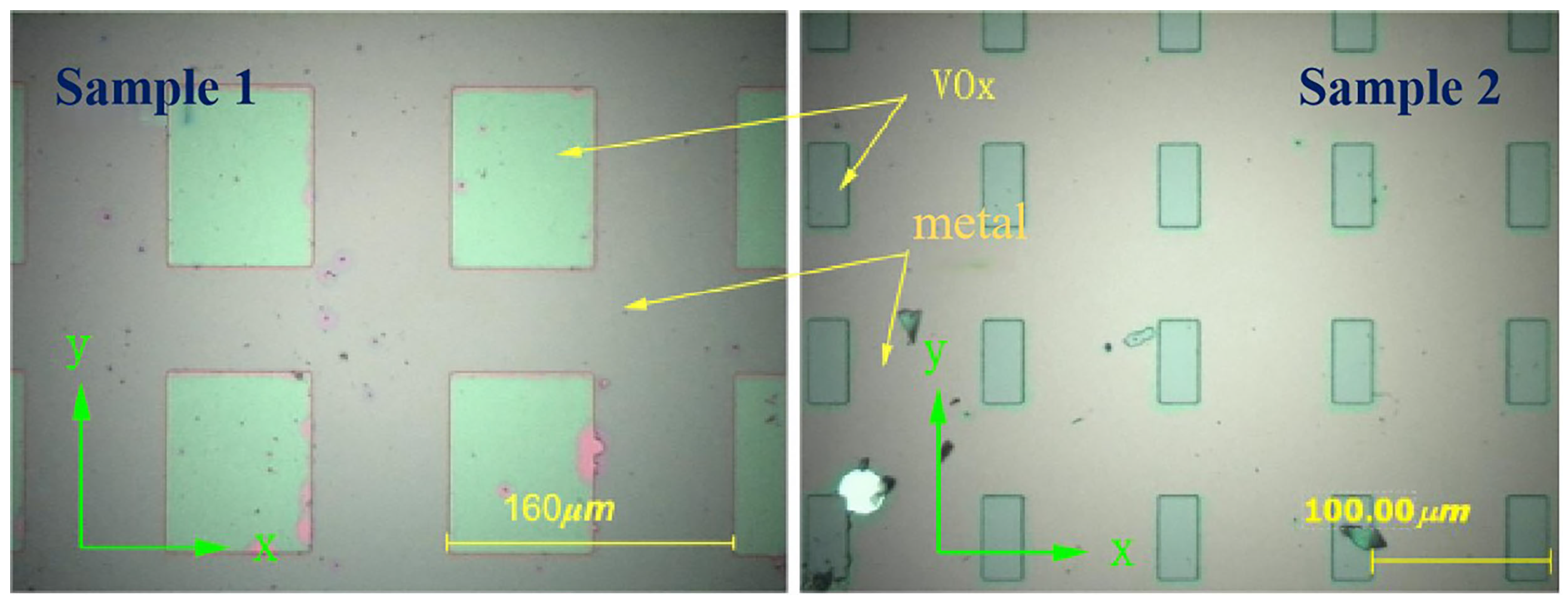
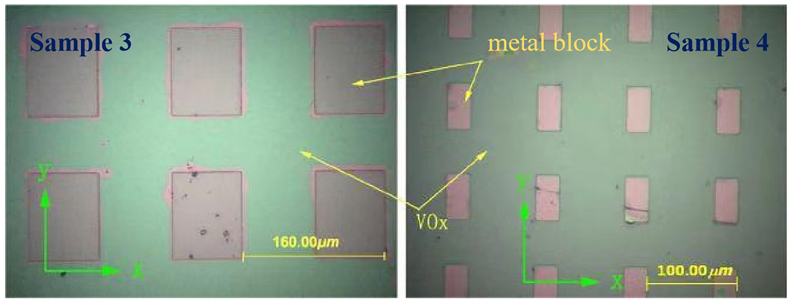
2.1. Preparation of Thin Films
2.2. Material with an SPP Structure
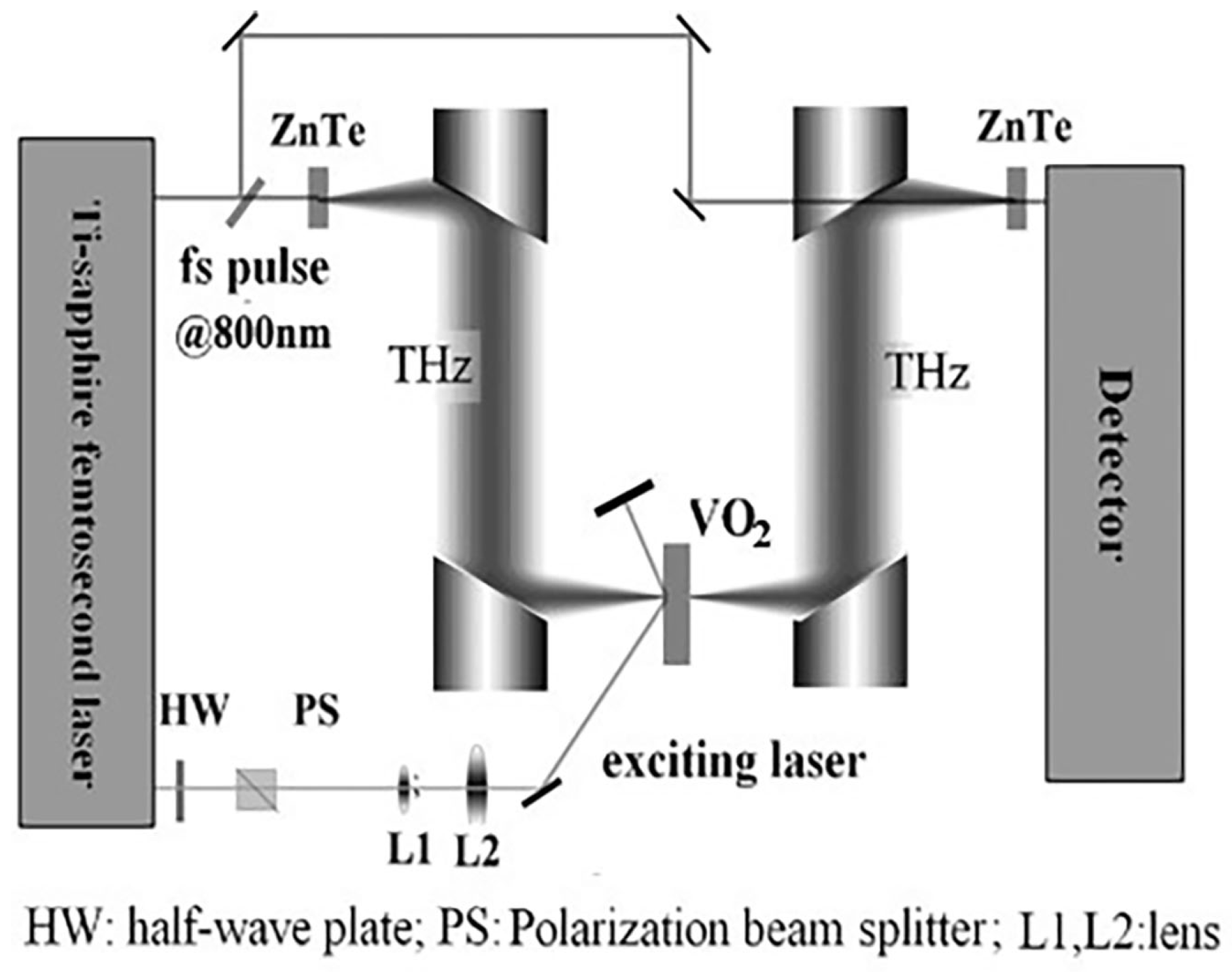
2.3. Terahertz Optical Experiments
3. Experimental Results and Discussion
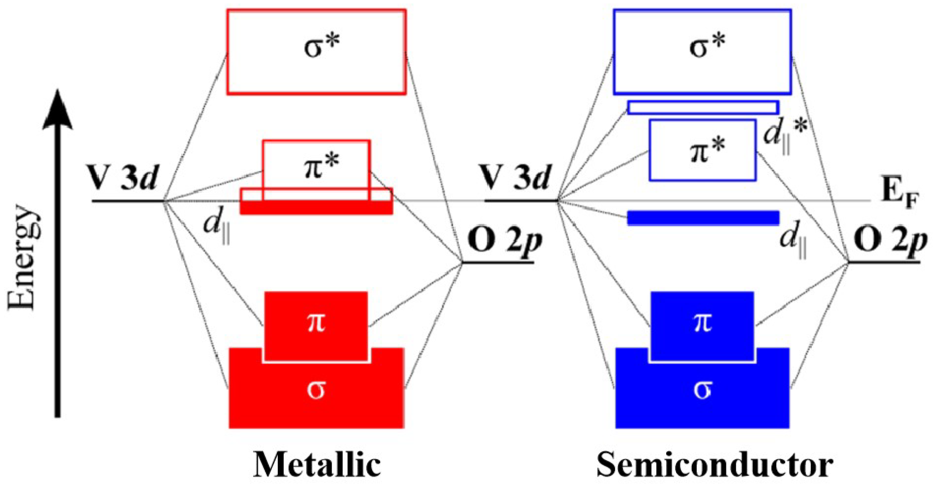
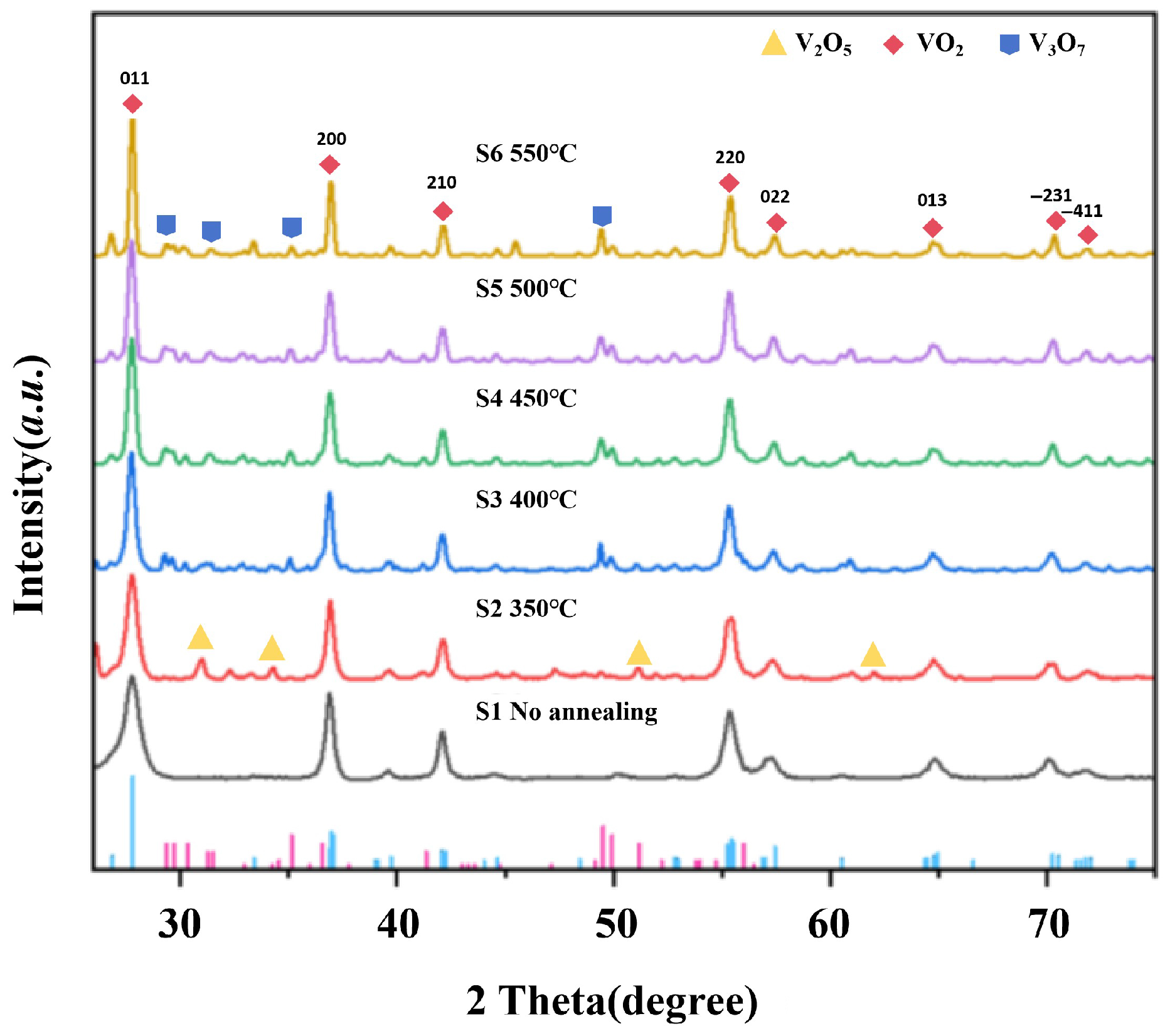
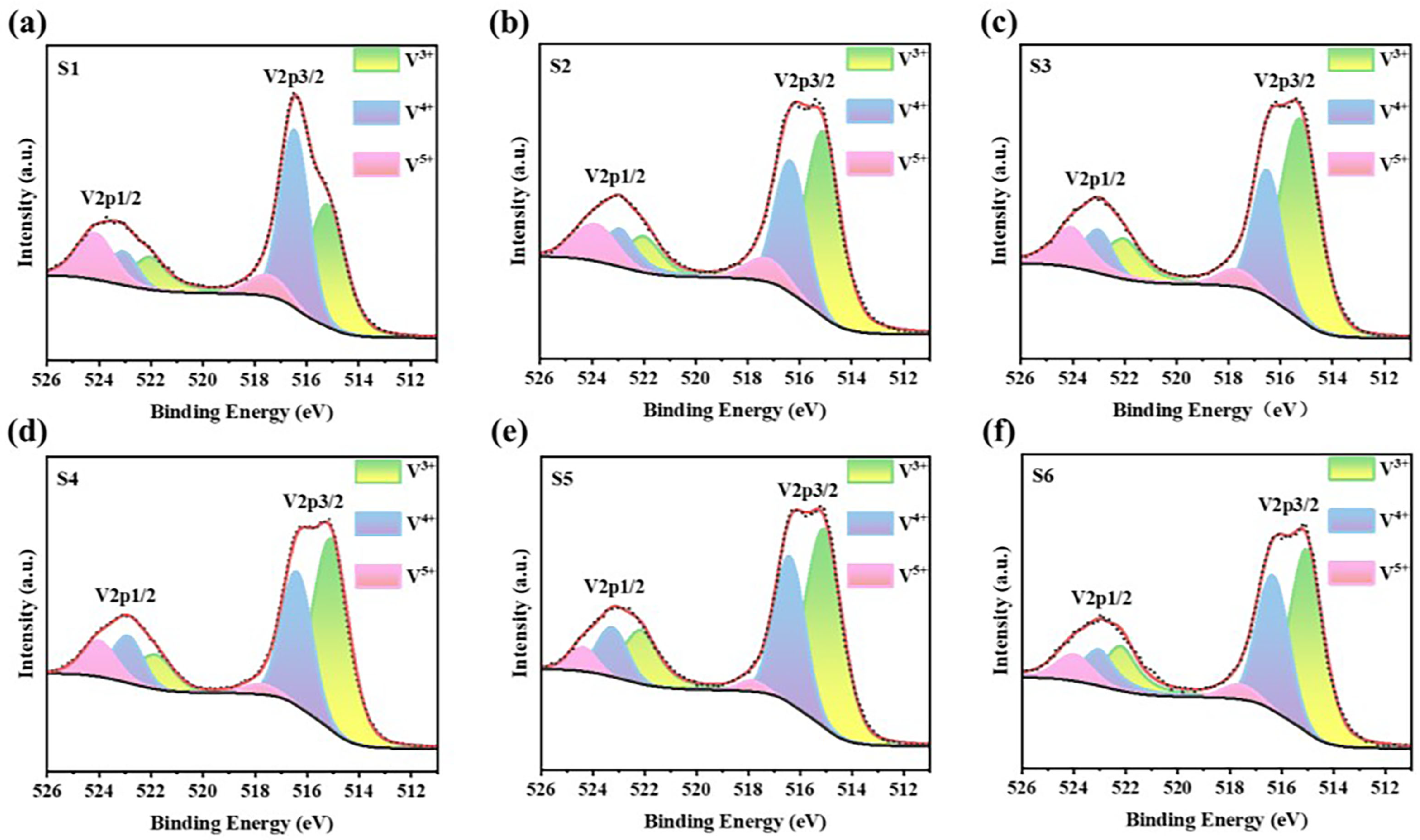
3.1. Composition and Surface Morphology Analysis of Nanoparticles
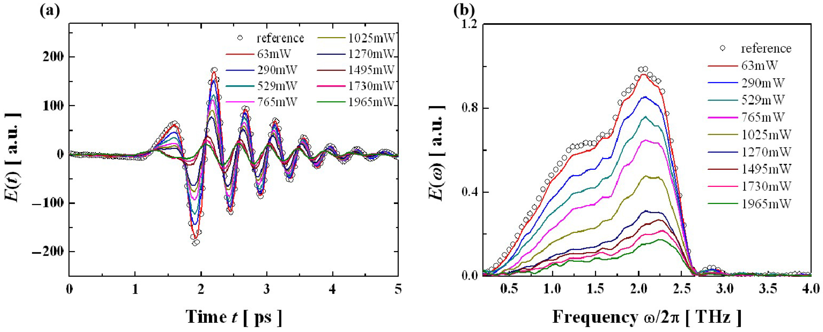
3.2. Test for Terahertz Optical Properties of Thin Films
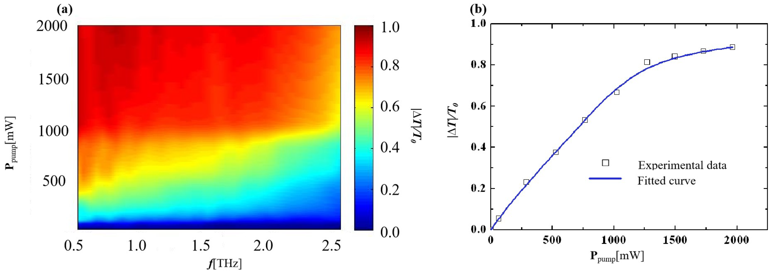
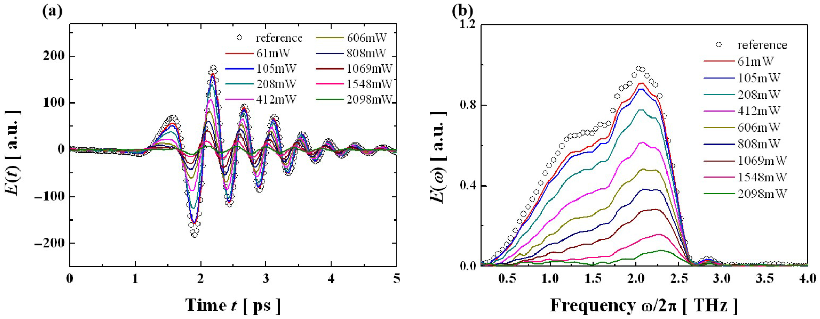
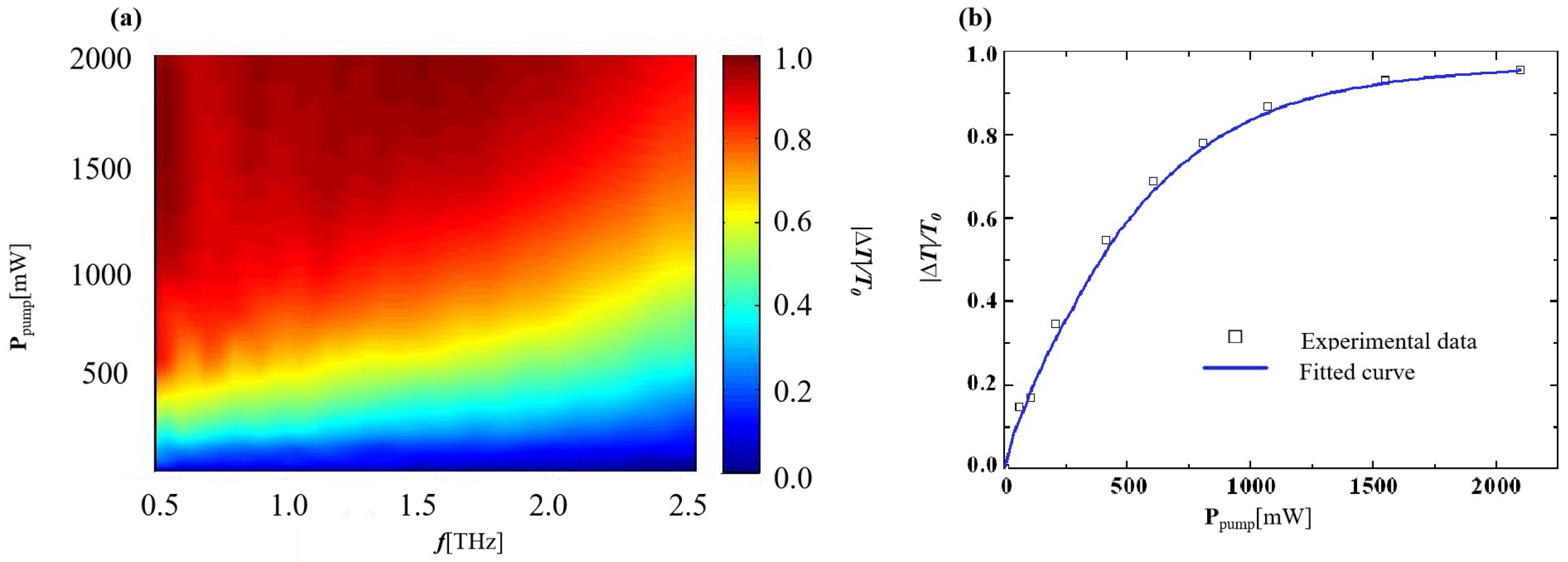
3.3. Modulating Terahertz Waves with a Femtosecond Laser Pulse with a Central Wavelength of 1040 nm
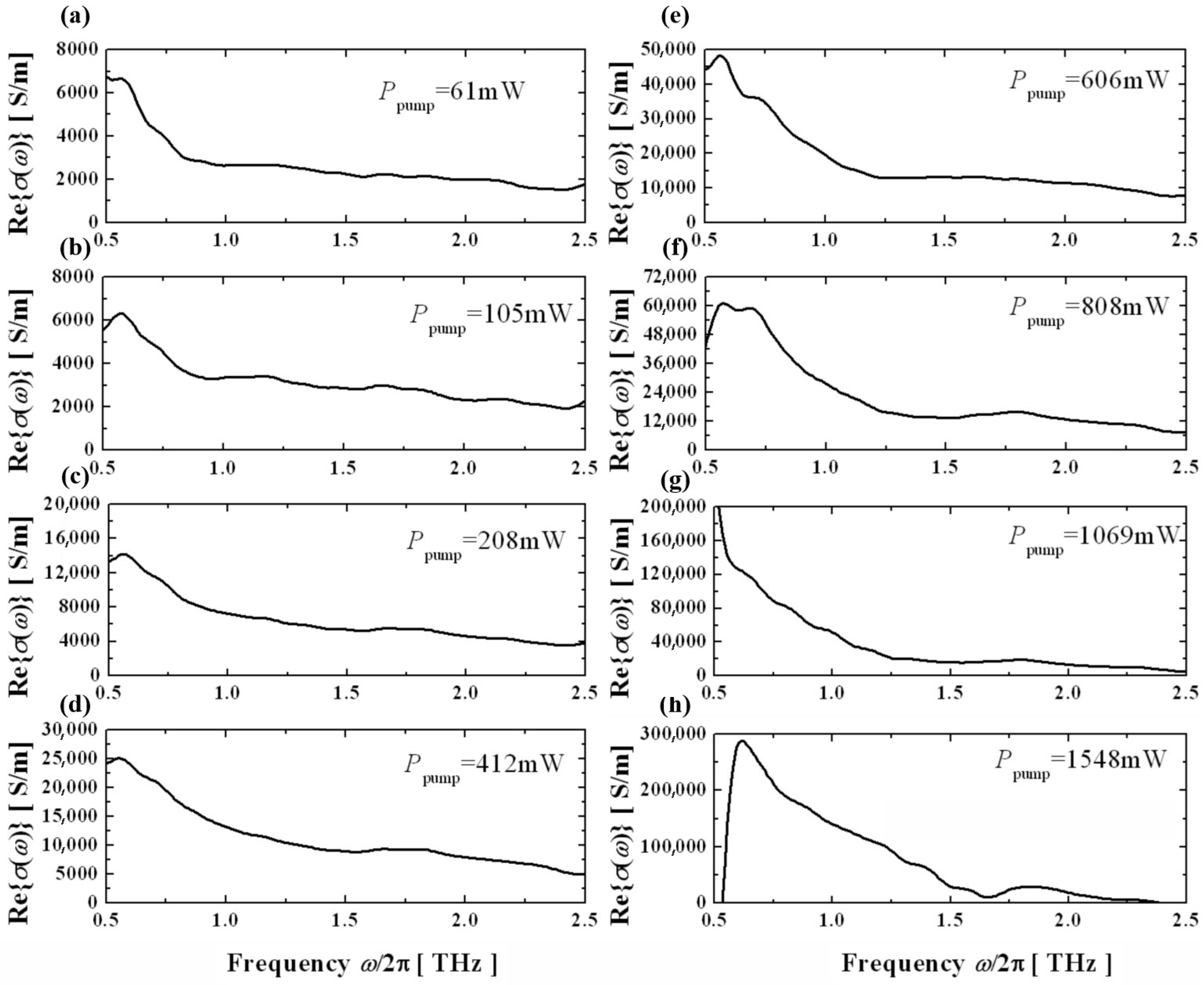
3.4. Metallic Property Analysis of Photoinduced Phase Change Silicon-Based Thin Films
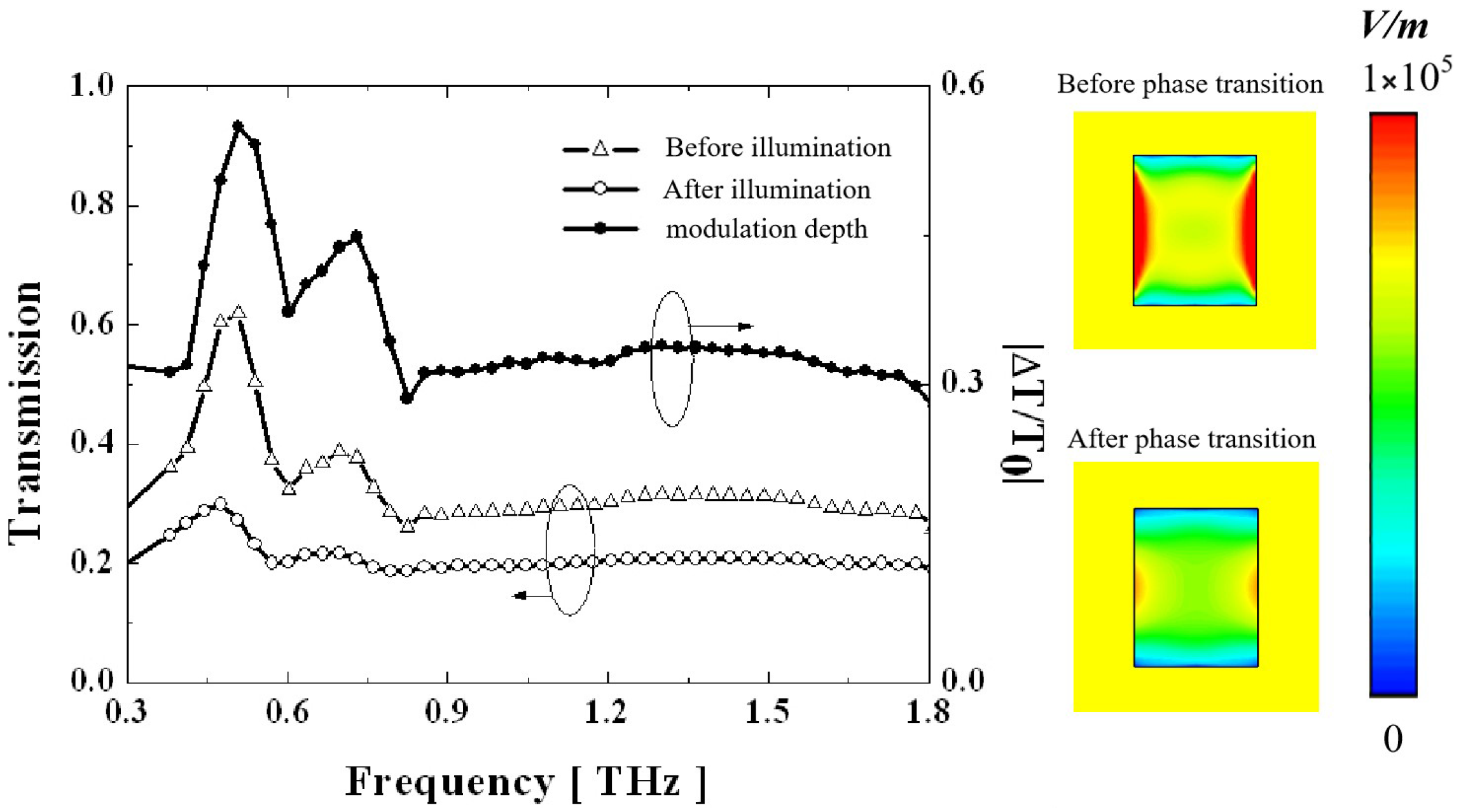
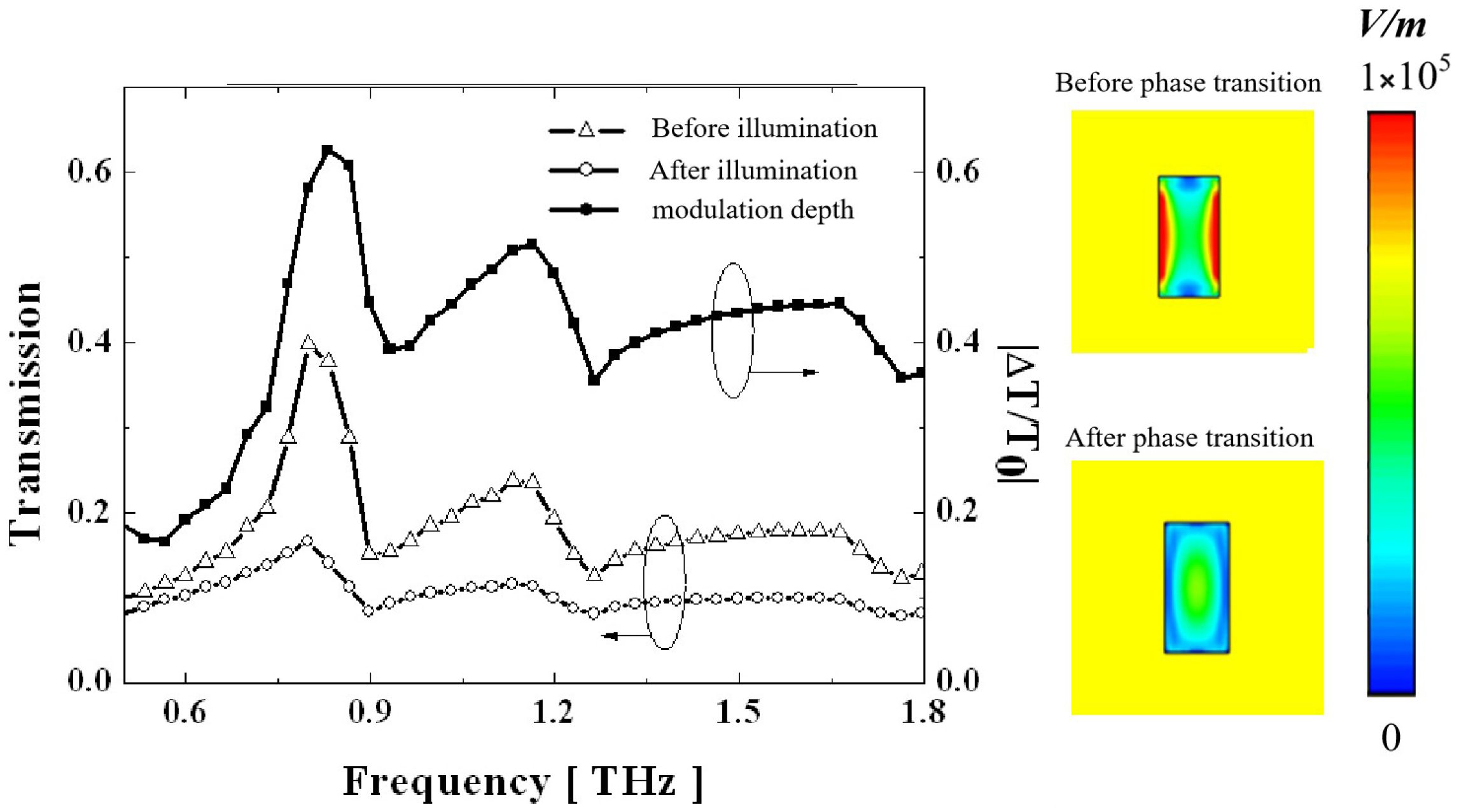
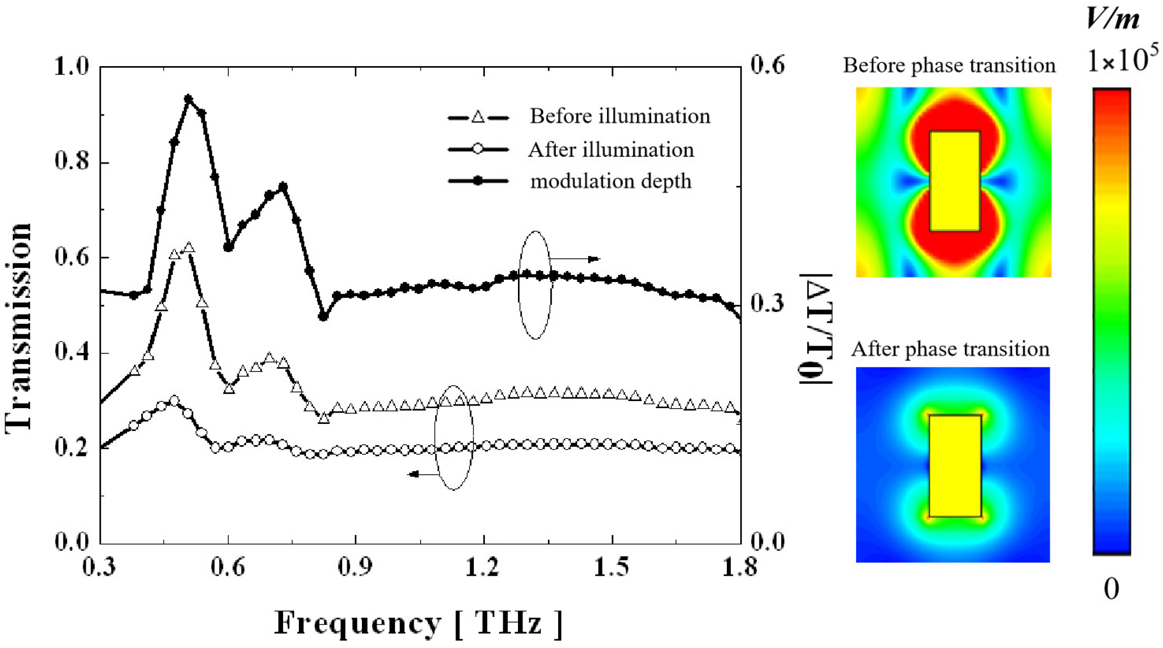
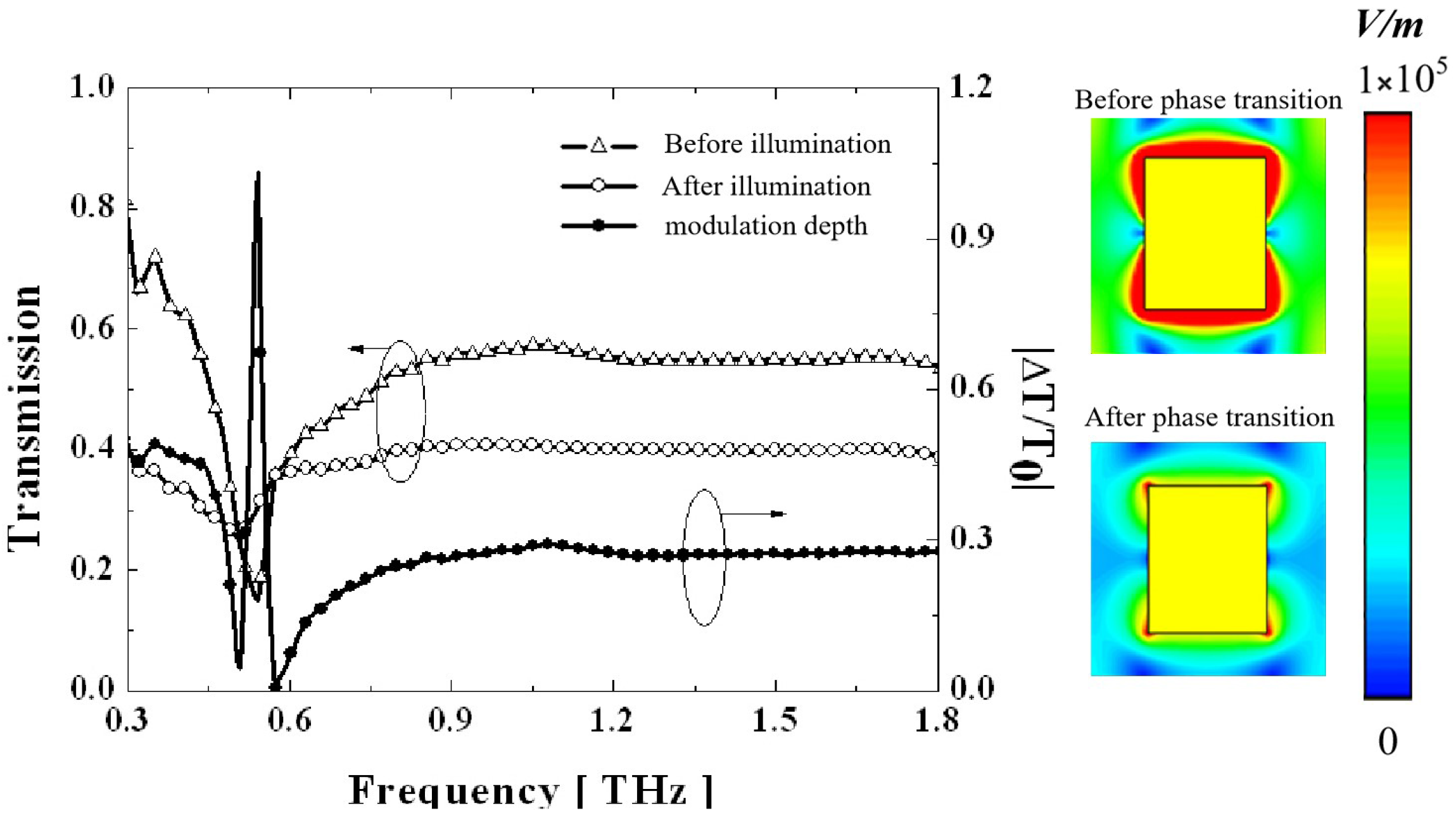
3.5. Terahertz Optical Test of Thin Films with an SPP Structure
4. Conclusions
Author Contributions
Funding
Institutional Review Board Statement
Informed Consent Statement
Data Availability Statement
Conflicts of Interest
References
- Zhang, Y.; Li, K.; Zhao, H. Intense terahertz radiation: Generation and application. Front. Optoelectron. 2021, 14, 4–36. [Google Scholar] [CrossRef]
- Buldt, J.; Stark, H.; Müller, M.; Grebing, C.; Jauregui, C.; Limpert, J. Gas-plasma-based generation of broadband terahertz radiation with 640 mW average power. Opt. Lett. 2021, 46, 5256–5259. [Google Scholar] [CrossRef] [PubMed]
- Carnio, B.N.; Moutanabbir, O.; Elezzabi, A.Y. Nonlinear photonic waveguides: A versatile platform for terahertz radiation generation (a review). Laser Photonics Rev. 2023, 17, 2200138. [Google Scholar] [CrossRef]
- Choi, W.J.; Armstrong, M.R.; Yoo, J.H.; Lee, T. Toward high-power terahertz radiation sources based on ultrafast lasers. J. Mater. Chem. 2024, 12, 9002–9011. [Google Scholar] [CrossRef]
- Jin, L.; Song, J.; Chen, L.; Yao, X.; Zhao, H.; Cheng, Q. VO2-based switchable thermal emitters using magnetic polaritons. J. Quant. Spectrosc. Radiat. Transf. 2024, 317, 108937. [Google Scholar] [CrossRef]
- Johnson, A.S.; Perez-Salinas, D.; Siddiqui, K.M.; Kim, S.; Choi, S.; Volckaert, K.; Majchrzak, P.E.; Ulstrup, S.; Agarwal, N.; Hallman, K.; et al. Ultrafast X-ray imaging of the light-induced phase transition in VO2. Nat. Phys. 2023, 19, 215–220. [Google Scholar] [CrossRef]
- Wang, Z.; Ji, X.; Dong, N.; Chen, C.; Yan, Z.; Cao, X.; Wang, J. Femtosecond laser-induced phase transition in VO2 films. Opt. Express 2022, 30, 47421–47429. [Google Scholar] [CrossRef]
- Hwang, I.H.; Jin, Z.; Park, C.I.; Sun, C.J.; Brewe, D.L.; Han, S.W. Electrical and structural properties of VO2 in an electric field. Curr. Appl. Phys. 2021, 30, 77–84. [Google Scholar] [CrossRef]
- Kumar, A.; Kumar, A.; Kandasami, A.; Singh, V.R. A comprehensive review on synthesis, phase transition, and applications of VO2. J. Supercond. Nov. Magn. 2024, 37, 475–498. [Google Scholar] [CrossRef]
- Wen, C.; Feng, L.; Li, Z.; Bai, J.; Wang, S.; Gao, X.; Wang, J.; Yao, W. A review of the preparation, properties and applications of VO2 thin films with the reversible phase transition. Front. Mater. 2024, 11, 1341518. [Google Scholar] [CrossRef]
- Yin, J.Y.; Ren, J.; Zhang, H.C.; Pan, B.C.; Cui, T.J. Broadband frequency-selective spoof surface plasmon polaritons on ultrathin metallic structure. Sci. Rep. 2015, 5, 8165. [Google Scholar] [CrossRef] [PubMed]
- Anwar, R.S.; Ning, H.; Mao, L. Recent advancements in surface plasmon polaritons-plasmonics in subwavelength structures in microwave and terahertz regimes. Digit. Commun. Netw. 2018, 4, 244–257. [Google Scholar] [CrossRef]
- Hamashima, K.; Wu, D.; Kishimoto, S.; Inoue, S.; Ohnuki, S. Selectivity of dominant surface plasmon polariton modes using thin metal waveguides with grating structures. Jpn. J. Appl. Phys. 2022, 61, 082002. [Google Scholar] [CrossRef]
- Gerasimov, V.; Nikitin, A.; Vanda, V.; Lemzyakov, A.; Azarov, I. Dispersion of Attenuation of Surface Plasmon Polaritons on Metal in the Terahertz Range. J. Infrared Millim. Terahertz Waves 2025, 46, 1–17. [Google Scholar] [CrossRef]
- Sun, Y.; Xu, C.; Zhou, W.; Qin, X.; Huang, Y.; Zhou, H.; Xu, N.; Wang, B.X. Transformation of Broadband Absorption to Electromagnetically-Induced Transparency Utilizing Terahertz Metamaterial-Based Phase Change Vanadium Dioxide. J. Electron. Mater. 2025, 54, 1407–1418. [Google Scholar] [CrossRef]
- Xiao, B.; Wang, X.; Gao, M. Research on VO2-based Absorbing/Polarization Conversion Terahertz Devices. Opt. Commun. 2025, 589, 131995. [Google Scholar] [CrossRef]
- Kim, J.; Kang, D.; Lee, E.J.; Kim, S.K.; Lee, M. High-performance dynamic thermal emitter based on Fabry- Pérot surface cavity comprising multi-phase VO2 layer. Int. J. Therm. Sci. 2025, 215, 109960. [Google Scholar] [CrossRef]
- Lu, X.; Yang, L.; Peng, W.; Yang, X. Metasurface based on VO2-Ge2Sb2Te5 with multi-modes: Cross-polarization conversion, reversible linear dichroism and absorption. Opt. Commun. 2025, 586, 131895. [Google Scholar] [CrossRef]
- Zhao, W.; Lv, X.; Xu, Q.; Wen, Z.; Shao, Y.; Liu, C.; Dai, N. Multifunctional terahertz metamaterials device based on a dual-tunable structure incorporating graphene and vanadium oxide. Nanoscale Adv. 2025, 7, 3817–3827. [Google Scholar] [CrossRef]
- Wilke, I.; Monahan, J.; Toroghi, S.; Rabiei, P.; Hine, G. Thin-film lithium niobate electro-optic terahertz wave detector. Sci. Rep. 2024, 14, 4822. [Google Scholar] [CrossRef]
- Morin, F. Oxides which show a metal-to-insulator transition at the Neel temperature. Phys. Rev. Lett. 1959, 3, 34. [Google Scholar] [CrossRef]
- Quackenbush, N.; Tashman, J.W.; Mundy, J.A.; Sallis, S.; Paik, H.; Misra, R.; Moyer, J.A.; Guo, J.H.; Fischer, D.A.; Woicik, J.C.; et al. Nature of the metal insulator transition in ultrathin epitaxial vanadium dioxide. Nano Lett. 2013, 13, 4857–4861. [Google Scholar] [CrossRef]
- Ebbesen, T.W.; Lezec, H.J.; Ghaemi, H.F.; Thio, T.; Wolff, P.A. Extraordinary optical transmission through sub-wavelength hole arrays. Nature 1998, 391, 667–669. [Google Scholar] [CrossRef]
- Mahmoud, M.; Turky, A.A.; Ahmed, M.; Fares, H. Loss effects on quantum surface plasmon polaritons excited by a traveling electron beam. Phys. Plasmas 2023, 30, 023101. [Google Scholar] [CrossRef]
- Gershuni, Y.; Epstein, I. In-plane exciton polaritons versus plasmon polaritons: Nonlocal corrections, confinement, and loss. Phys. Rev. B 2024, 109, L121408. [Google Scholar] [CrossRef]
- Xiang, W.; Le Drogoff, B.; Chaker, M. An innovative method to achieve large-scale high-quality VO2 thin films: Oxidation of vanadium nitride material deposited by sputtering. Appl. Surf. Sci. 2023, 633, 157607. [Google Scholar] [CrossRef]
- Zhang, C.; Gunes, O.; Wen, S.J.; Yang, Q.; Kasap, S. Effect of substrate temperature on the structural, optical and electrical properties of DC magnetron sputtered VO2 thin films. Materials 2022, 15, 7849. [Google Scholar] [CrossRef]
- Lintao, L.; Weijia, G.; Shijie, Y.; Ping, L.; Jialun, D.; Yuping, Z.; Haitao, W.; Yueguang, C.; Zhenxing, Y. Microstructure, Raman spectroscopy, THz time domain spectrum and microwave dielectric properties of Li2Ti1-x (Zn1/3Ta2/3) xO3 ceramics. Ceram. Int. 2023, 49, 6864–6872. [Google Scholar] [CrossRef]
- Koch, M.; Mittleman, D.M.; Ornik, J.; Castro-Camus, E. Terahertz time-domain spectroscopy. Nat. Rev. Methods Prim. 2023, 3, 48. [Google Scholar] [CrossRef]
- Mitra, S.; Avazpour, L.; Knezevic, I. Terahertz conductivity of two-dimensional materials: A review. J. Phys. Condens. Matter 2025, 37, 133005. [Google Scholar] [CrossRef]
- Wang, G.; Wu, R.; Zhang, L.; Zhang, C.; Zhang, X.C. Coherent detection of pulsed terahertz waves in solid, gaseous, and liquid media. Fundam. Res. 2024, 5, 516–525. [Google Scholar] [CrossRef]
- Liang, J.; Lou, Q.; Wu, W.; Wang, K.; Xuan, C. NO2 gas sensing performance of a VO2 (B) ultrathin vertical nanosheet array: Experimental and DFT investigation. Acs Appl. Mater. Interfaces 2021, 13, 31968–31977. [Google Scholar] [CrossRef]
- Silversmit, G.; Depla, D.; Poelman, H.; Marin, G.B.; De Gryse, R. Determination of the V2p XPS binding energies for different vanadium oxidation states (V5+ to V0+). J. Electron Spectrosc. Relat. Phenom. 2004, 135, 167–175. [Google Scholar] [CrossRef]
- Zhang, Z.; Zuo, F.; Wan, C.; Dutta, A.; Kim, J.; Rensberg, J.; Nawrodt, R.; Park, H.H.; Larrabee, T.J.; Guan, X.; et al. Evolution of metallicity in vanadium dioxide by creation of oxygen vacancies. Phys. Rev. Appl. 2017, 7, 034008. [Google Scholar] [CrossRef]
- Strand, J.; Chulkov, S.K.; Watkins, M.B.; Shluger, A.L. First principles calculations of optical properties for oxygen vacancies in binary metal oxides. J. Chem. Phys. 2019, 150, 044702. [Google Scholar] [CrossRef]
- Popov, A.; Kotomin, E.; Maier, J. Basic properties of the F-type centers in halides, oxides and perovskites. Nucl. Instruments Methods Phys. Res. Sect. B Beam Interact. Mater. Atoms 2010, 268, 3084–3089. [Google Scholar] [CrossRef]
- Cooke, D.G.; Hegmann, F.A.; Mazur, Y.I.; Ma, W.Q.; Wang, X.; Wang, Z.M.; Salamo, G.J.; Xiao, M.; Mishima, T.D.; Johnson, M.B. Anisotropic photoconductivity of InGaAs quantum dot chains measured by terahertz pulse spectroscopy. Appl. Phys. Lett. 2004, 85, 3839–3841. [Google Scholar] [CrossRef]
- Cooke, D.G.; Hegmann, F.A.; Young, E.C.; Tiedje, T. Electron mobility in dilute GaAs bismide and nitride alloys measured by time-resolved terahertz spectroscopy. Appl. Phys. Lett. 2006, 89, 1608. [Google Scholar] [CrossRef]
- Glover, R.E.; Tinkham, M. Transmission of Superconducting Films at Millimeter-Microwave and Far Infrared Frequencies. Phys. Rev. 1956, 104, 844–845. [Google Scholar] [CrossRef]
- Hegmann, F.A.; Ostroverkhova, O.; Cooke, D.G. Probing organic semiconductors with terahertz pulses. In Photophysics of Molecular Materials: From Single Molecules to Single Crystals; John Wiley & Sons: Hoboken, NJ, USA, 2005; pp. 367–428. [Google Scholar]
- Tu, J.; Homes, C.; Strongin, M. Optical Properties of Ultrathin Films: Evidence for a Dielectric Anomaly at the Insulator-to-Metal Transition. Phys. Rev. Lett. 2003, 90, 017402. [Google Scholar] [CrossRef]
- Schmuttenmaer, C.A. Exploring dynamics in the far-infrared with terahertz spectroscopy. Chem. Rev. 2004, 104, 1759–1780. [Google Scholar] [CrossRef]
- Wang, C.; Tan, S.; Lin, X.; Chen, H.; Gao, F. Terahertz plasmonic metagrating design simultaneously enabling broadband extraordinary transmission and field enhancement. Prog. Electromagn. Res. 2023, 177, 85–94. [Google Scholar] [CrossRef]

| Samples | (%) | (%) | (%) |
|---|---|---|---|
| S1 | 45.60 | 47.34 | 7.06 |
| S2 | 60.85 | 31.78 | 7.37 |
| S3 | 64.69 | 31.72 | 3.59 |
| S4 | 63.00 | 36.85 | 0.15 |
| S5 | 61.80 | 36.05 | 2.15 |
| S6 | 60.31 | 35.53 | 4.16 |
Disclaimer/Publisher’s Note: The statements, opinions and data contained in all publications are solely those of the individual author(s) and contributor(s) and not of MDPI and/or the editor(s). MDPI and/or the editor(s) disclaim responsibility for any injury to people or property resulting from any ideas, methods, instructions or products referred to in the content. |
© 2025 by the authors. Licensee MDPI, Basel, Switzerland. This article is an open access article distributed under the terms and conditions of the Creative Commons Attribution (CC BY) license (https://creativecommons.org/licenses/by/4.0/).
Share and Cite
Chen, T.; Zhang, Q.; Wang, J.; Liang, J.; Zhou, W. Research on the Terahertz Modulation Performance of VO2 Thin Films with Surface Plasmon Polaritons Structure. Coatings 2025, 15, 838. https://doi.org/10.3390/coatings15070838
Chen T, Zhang Q, Wang J, Liang J, Zhou W. Research on the Terahertz Modulation Performance of VO2 Thin Films with Surface Plasmon Polaritons Structure. Coatings. 2025; 15(7):838. https://doi.org/10.3390/coatings15070838
Chicago/Turabian StyleChen, Tao, Qi Zhang, Jin Wang, Jiran Liang, and Weibin Zhou. 2025. "Research on the Terahertz Modulation Performance of VO2 Thin Films with Surface Plasmon Polaritons Structure" Coatings 15, no. 7: 838. https://doi.org/10.3390/coatings15070838
APA StyleChen, T., Zhang, Q., Wang, J., Liang, J., & Zhou, W. (2025). Research on the Terahertz Modulation Performance of VO2 Thin Films with Surface Plasmon Polaritons Structure. Coatings, 15(7), 838. https://doi.org/10.3390/coatings15070838