

A Comprehensive Review on Aero-Materials: Present and Future Perspectives

 , ,
, , 

Abstract
1. Introduction
2. Semiconductor Aero-Materials
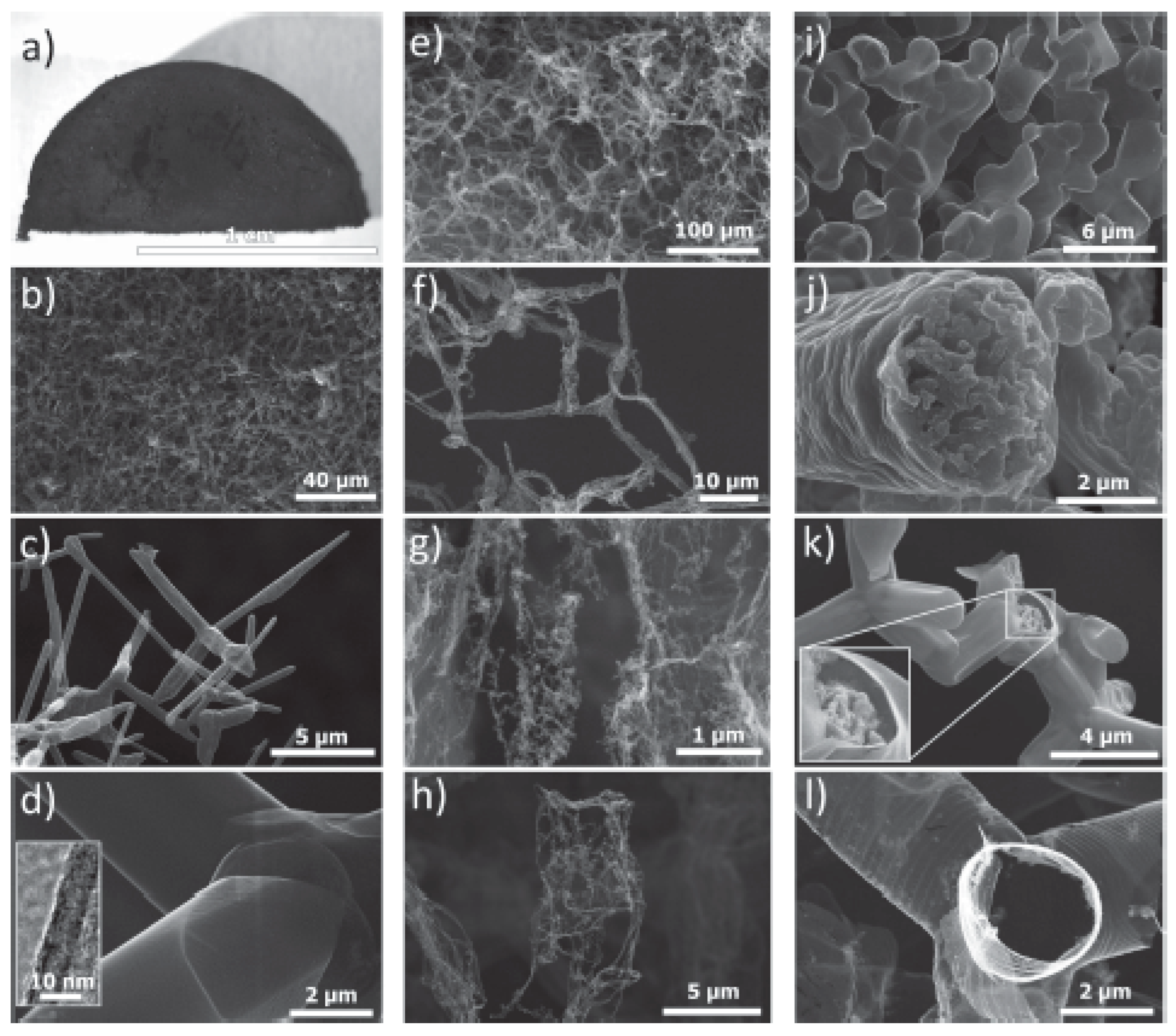
2.1. ZnO Tetrapods Synthesis Methods
2.1.1. Combustion Method (CM)
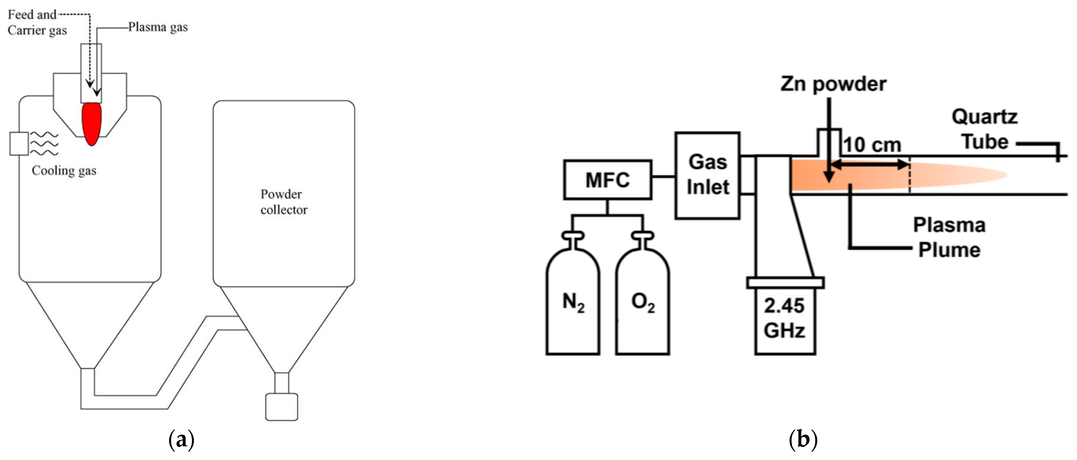
2.1.2. DC Thermal Plasma
2.1.3. Microwave
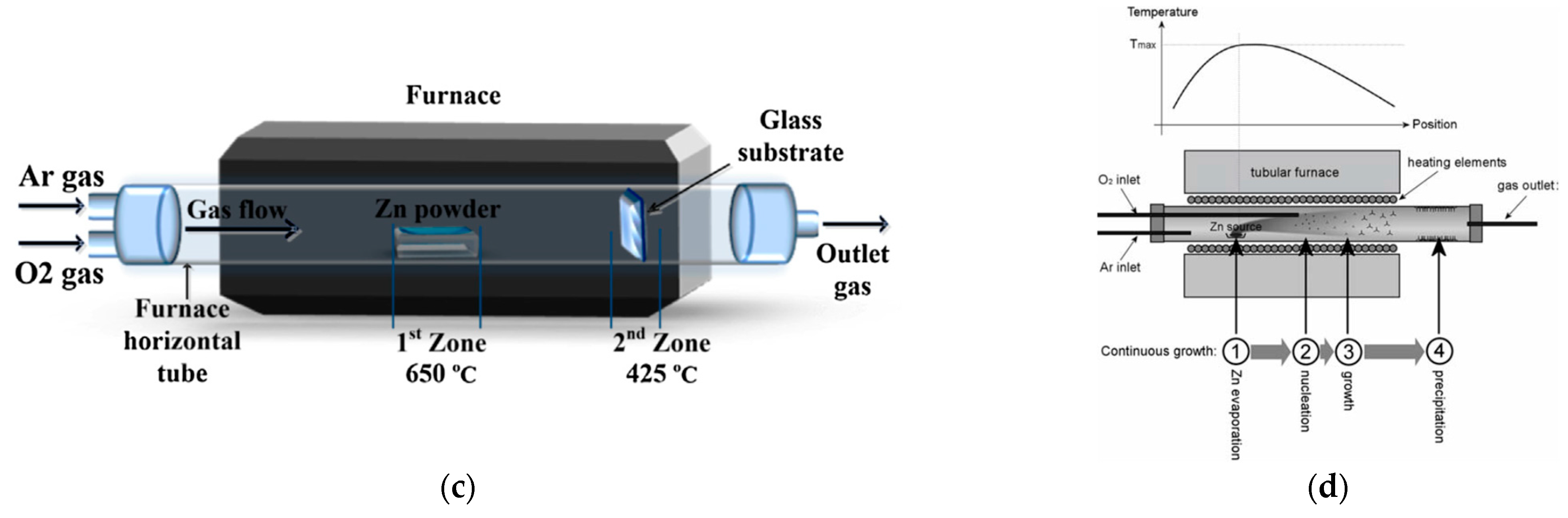
2.1.4. Thermal Oxidation (TO)
2.1.5. Flame Transport Synthesis (FTS)
2.1.6. Vapor Phase Growth (VPG)
2.1.7. Chemical Vapor Deposition (CVD)

| Synthesis Methods | Advantages | Material Purity/Precursor | Investigated Properties | Application/Proposed Domain | Ref. |
|---|---|---|---|---|---|
| MCM | No volatile salts, which makes the process cheap | 99.995% bulk industrial, metal Zn | Morpho-structural, optical, luminescence, photoluminescence, electrical conductivity | Growth mechanism, shock-resistance, optical, technological, nanodevices, and nanosensors | [62,63,64] |
| DC | Synthesis of various oxide nanoparticles at low cost and high yield | 95%–99% metal zinc | Morpho-structural, photostability, optical, current–voltage, electrochemical, and photocurrent–voltage | Photocatalytic, photovoltaic process, and photoelectrode | [66,67,68,69] |
| Microwave | Synthesis quickly and low energy consumption | 99.9% Zn powder | Morpho-structural, humidity sensing, photosensitivity, optical, photocatalytic, and recyclability | Industrial activity, degradation of organic dyes and flexible photosensors | [70,71] |
| TO | Simple and low-cost method, depending on the substrate | 99.99% Zn powder | Morpho-structural, optical, photoluminescence, and kinetics | Gas sensor and UV photodetection | [74,76,78,79] |
| FTS | Facile and cost-efficient | Zn microparticles | Morpho-structural, optical, photocatalytic, fluorescently | Nanosensing devices, gas sensor, sacrificial template | [80,81,88] |
| VPG | Easy for different ZnO nanostructures, but the morphologies are mixed together | 99.999% powder and Zn foil | Morpho-structural, conductance, relative humidity, sensor response | Gas sensors, optoelectronic | [75,83] |
| CVD | Low-cost method compared with the PVD method | 99.999% Zn powder | Morpho-structural, optical, photoluminescence, growth mechanisms, luminescence | Nanooptics, nanoelectronics, nanodevices | [85,86,87] |
2.2. Type of Aero-Materials
2.2.1. Aerographite

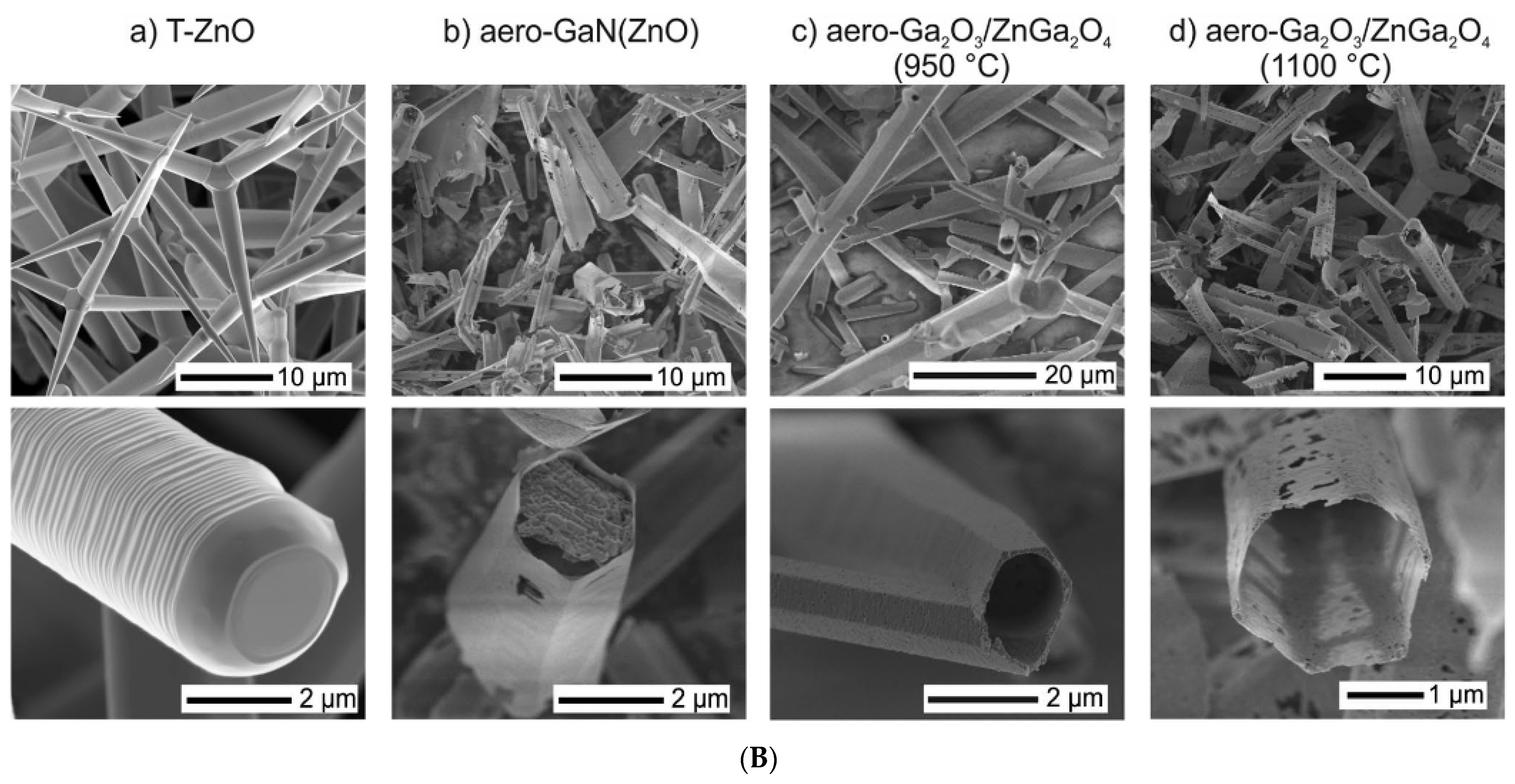
2.2.2. Aero-β-Ga2O3
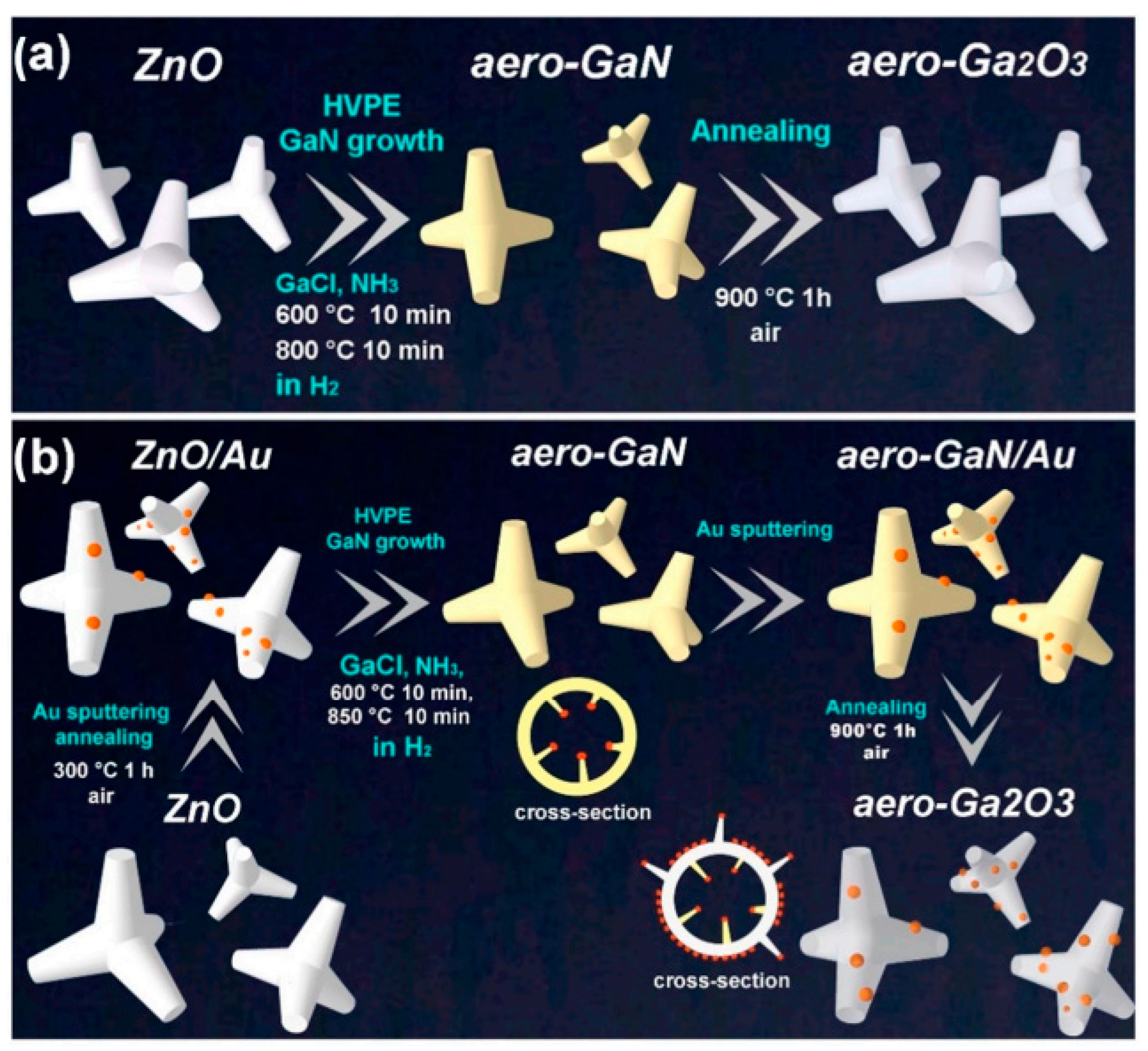
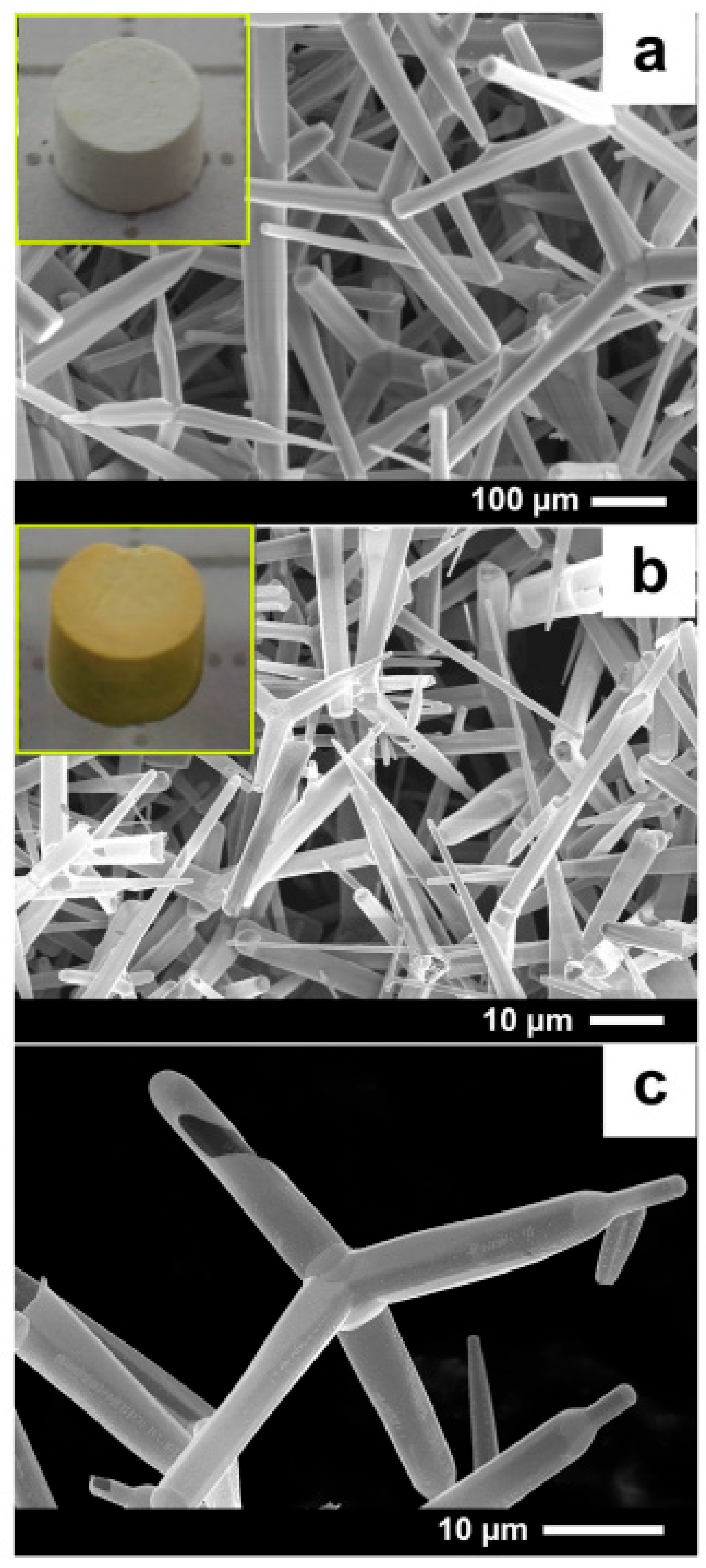
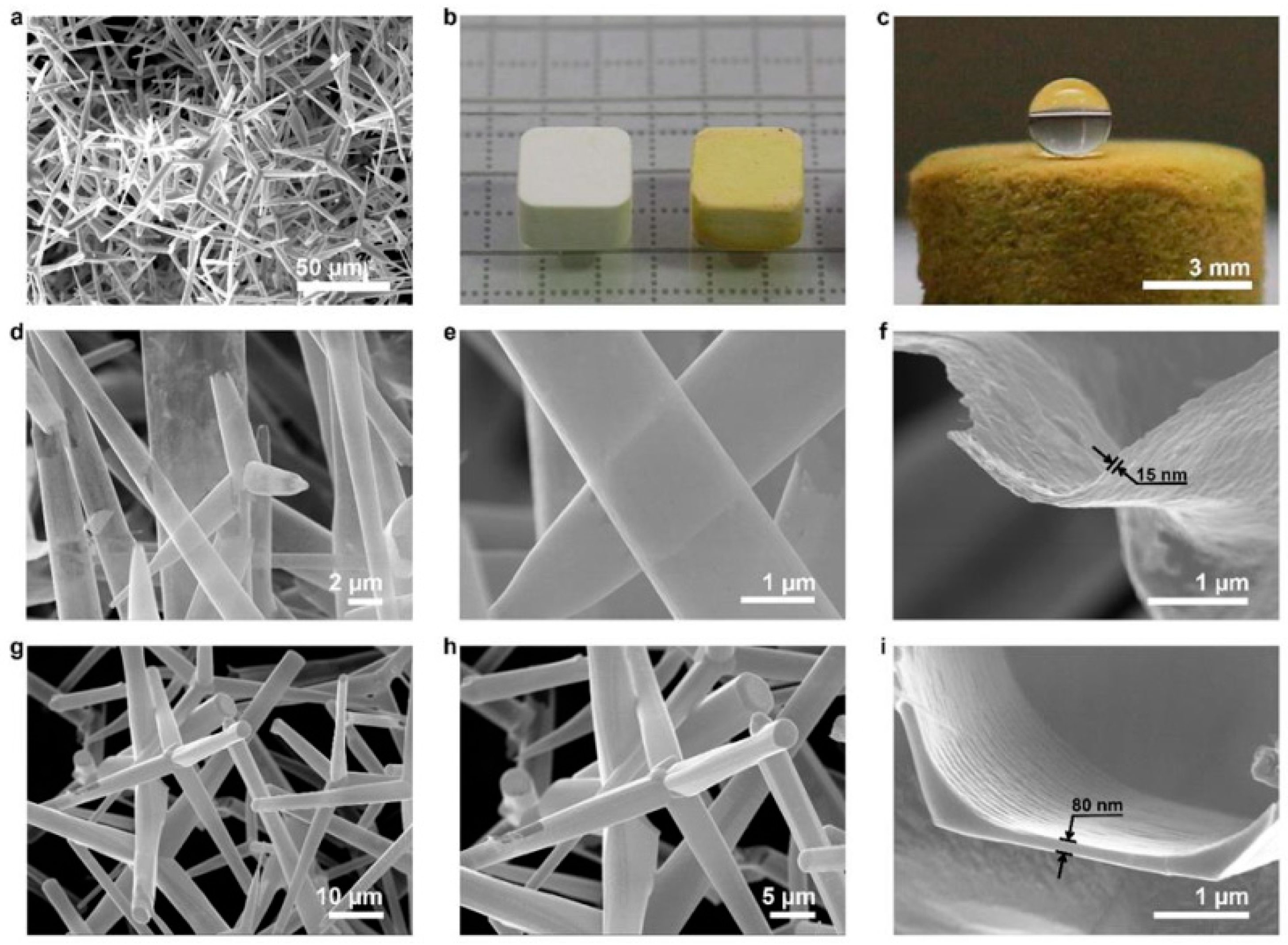
2.2.3. Aero-GaN
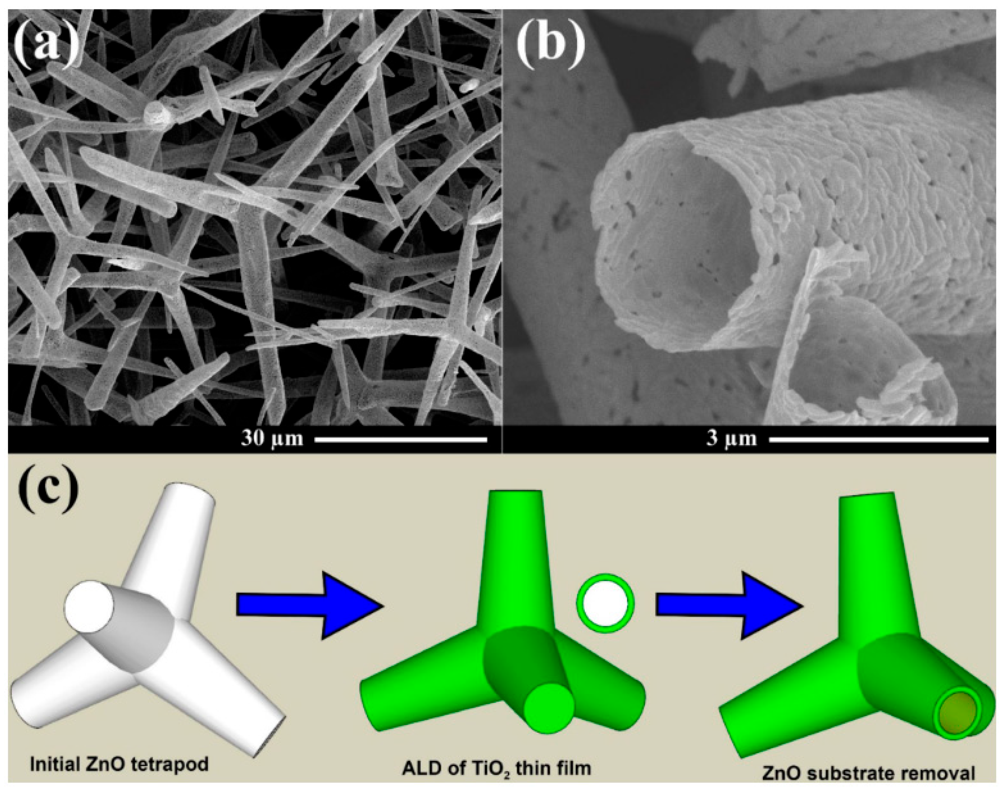
2.2.4. Aero-TiO2
2.2.5. Other Aero-Materials
3. Conclusions and Future Perspectives
- Control of structural and synthesis method—The synthesis methods that use ZnO(T) as sacrificial templates suffer from limited control over size distribution, pore connectivity, and wall thickness. Improved methodologies for predictable nano- and microscale structural control are required. Moreover, most present synthesis techniques (e.g., HVPE, CVD, and TO) demand high temperatures and possibly toxic reagents; thus, developing low-energy, sustainable, and solvent-free methods is crucial for environmental protection and energy-efficient production.
- Surface functionalization—Many applications require specific functional groups or surface changes (e.g., biosensing and catalysis); thus, more research on post-synthesis functionalization techniques that maintain structural integrity is needed.
- Application level and testing—For application in real-world devices, semiconductor aero-materials must be tested under severe temperatures, cyclic stress, humidity, and chemically severe environments. For applications on specific prototypes, more effort is required to progress from proof-of-concept research to practical prototypes, and more tests for biomedical applications.
Funding
Institutional Review Board Statement
Informed Consent Statement
Data Availability Statement
Conflicts of Interest
References
- Li, W.; Tekell, M.; Liu, C.; Hethcock, J.; Fan, D. Flexible All-Solid-State Supercapacitors of High Areal Capacitance Enabled by Porous Graphite Foams with Diverging Microtubes. Adv. Funct. Mater. 2018, 28, 1800601. [Google Scholar] [CrossRef]
- Tang, C.; Wang, H.-F.; Huang, J.-Q.; Qian, W.; Wei, F.; Qiao, S.-Z.; Zhang, Q. 3D Hierarchical Porous Graphene-Based Energy Materials: Synthesis, Functionalization, and Application in Energy Storage and Conversion. Electrochem. Energy Rev. 2019, 2, 332–371. [Google Scholar] [CrossRef]
- Devendran, A.; Nagai, A. Recent advancements in 3D porous graphene-based electrode materials for electrochemical energy storage applications. Mater. Adv. 2023, 4, 2524–2543. [Google Scholar] [CrossRef]
- Ansari, S.P.; Husain, A.; Shariq, M.U.; Ansari, M.O. Chapter 5—Conducting polymer-based aerogels for energy and environmental remediation. In Advances in Aerogel Composites for Environmental Remediation; Khan, A.A.P., Ansari, M.O., Khan, A., Asiri, A.M., Eds.; Elsevier: Amsterdam, The Netherlands, 2021; pp. 75–86. [Google Scholar] [CrossRef]
- Li, W.; Tekell, M.C.; Huang, Y.; Bertelsmann, K.; Lau, M.; Fan, D. Synergistic High-Rate Solar Steaming and Mercury Removal with MoS2/C @ Polyurethane Composite Sponges. Adv. Energy Mater. 2018, 8, 1802108. [Google Scholar] [CrossRef]
- Sun, X.; Xue, B.; Tian, Y.; Qin, S.; Xie, L. 3D porous poly(l-lactic acid) materials with controllable multi-scale microstructures and their potential application in oil-water separation. Appl. Surf. Sci. 2018, 462, 633–640. [Google Scholar] [CrossRef]
- Siddique, J.A.; Ansari, S.P.; Yadav, M. Chapter 4—Carbon aerogel composites for gas sensing. In Advances in Aerogel Composites for Environmental Remediation; Khan, A.A.P., Ansari, M.O., Khan, A., Asiri, A.M., Eds.; Elsevier: Amsterdam, The Netherlands, 2021; pp. 49–73. [Google Scholar] [CrossRef]
- Wang, Z.; Tammela, P.; Strømme, M.; Nyholm, L. Cellulose-based Supercapacitors: Material and Performance Considerations. Adv. Energy Mater. 2017, 7, 1700130. [Google Scholar] [CrossRef]
- Yang, M.; Choy, K.-l. A nature-derived, flexible and three dimensional (3D) nano-composite for chronic wounds pH monitoring. Mater. Lett. 2021, 288, 129335. [Google Scholar] [CrossRef]
- Asmussen, R.M.; Matyáš, J.; Qafoku, N.P.; Kruger, A.A. Silver-functionalized silica aerogels and their application in the removal of iodine from aqueous environments. J. Hazard. Mater. 2019, 379, 119364. [Google Scholar] [CrossRef]
- Chang, Q.; Huang, L.; Wang, J.; Ma, Z.; Li, P.; Yan, Y.; Zhu, J.; Xu, S.; Shen, L.; Chen, Q.; et al. Nanoarchitecture of variable sized graphene nanosheets incorporated into three-dimensional graphene network for dye sensitized solar cells. Carbon 2015, 85, 185–193. [Google Scholar] [CrossRef]
- Li, W.; Huang, Y.; Liu, Y.; Tekell, M.C.; Fan, D. Three dimensional nanosuperstructures made of two-dimensional materials by design: Synthesis, properties, and applications. Nano Today 2019, 29, 100799. [Google Scholar] [CrossRef]
- Zhao, Q.; Chen, Y.; Qin, B.; Hu, C.; Xia, G.; Hao, L.; Ping, X. Synthesis of Three-Dimensional Carbon Nanosheets and Its Flux Pinning Mechanisms in C-Doped MgB2 Superconductors. Materials 2022, 15, 7530. [Google Scholar] [CrossRef] [PubMed]
- Wang, X.; Ahmad, M.; Sun, H. Three-Dimensional ZnO Hierarchical Nanostructures: Solution Phase Synthesis and Applications. Materials 2017, 10, 1304. [Google Scholar] [CrossRef]
- Owuor, P.S.; Park, O.-K.; Woellner, C.F.; Jalilov, A.S.; Susarla, S.; Joyner, J.; Ozden, S.; Duy, L.; Villegas Salvatierra, R.; Vajtai, R.; et al. Lightweight Hexagonal Boron Nitride Foam for CO2 Absorption. ACS Nano 2017, 11, 8944–8952. [Google Scholar] [CrossRef]
- Mekonnen, B.T.; Ding, W.; Liu, H.; Guo, S.; Pang, X.; Ding, Z.; Seid, M.H. Preparation of aerogel and its application progress in coatings: A mini overview. J. Leather Sci. Eng. 2021, 3, 25. [Google Scholar] [CrossRef]
- Ansari, M.O.; Khan, A.A.P.; Ansari, M.S.; Khan, A.; Kulkarni, R.M.; Bhamare, V.S. Chapter 1—Aerogel and its composites: Fabrication and properties. In Advances in Aerogel Composites for Environmental Remediation; Khan, A.A.P., Ansari, M.O., Khan, A., Asiri, A.M., Eds.; Elsevier: Amsterdam, The Netherlands, 2021; pp. 1–17. [Google Scholar] [CrossRef]
- Jafari, S.; Derakhshankhah, H.; Alaei, L.; Fattahi, A.; Varnamkhasti, B.S.; Saboury, A.A. Mesoporous silica nanoparticles for therapeutic/diagnostic applications. Biomed. Pharmacother. 2019, 109, 1100–1111. [Google Scholar] [CrossRef] [PubMed]
- Noman, M.T.; Amor, N.; Ali, A.; Petrik, S.; Coufal, R.; Adach, K.; Fijalkowski, M. Aerogels for Biomedical, Energy and Sensing Applications. Gels 2021, 7, 264. [Google Scholar] [CrossRef]
- Tiginyanu, I.; Ghimpu, L.; Gröttrup, J.; Postolache, V.; Mecklenburg, M.; Stevens-Kalceff, M.A.; Ursaki, V.; Payami, N.; Feidenhansl, R.; Schulte, K.; et al. Strong light scattering and broadband (UV to IR) photoabsorption in stretchable 3D hybrid architectures based on Aerographite decorated by ZnO nanocrystallites. Sci. Rep. 2016, 6, 32913. [Google Scholar] [CrossRef]
- Mecklenburg, M.; Schuchardt, A.; Mishra, Y.K.; Kaps, S.; Adelung, R.; Lotnyk, A.; Kienle, L.; Schulte, K. Aerographite: Ultra Lightweight, Flexible Nanowall, Carbon Microtube Material with Outstanding Mechanical Performance. Adv. Mater. 2012, 24, 3486–3490. [Google Scholar] [CrossRef]
- Marx, J.; Lewke, M.R.D.; Smazna, D.; Mishra, Y.K.; Adelung, R.; Schulte, K.; Fiedler, B. Processing, growth mechanism and thermodynamic calculations of carbon foam with a hollow tetrapodal morphology—Aerographite. Appl. Surf. Sci. 2019, 470, 535–542. [Google Scholar] [CrossRef]
- Meija, R.; Signetti, S.; Schuchardt, A.; Meurisch, K.; Smazna, D.; Mecklenburg, M.; Schulte, K.; Erts, D.; Lupan, O.; Fiedler, B.; et al. Nanomechanics of individual aerographite tetrapods. Nat. Commun. 2017, 8, 14982. [Google Scholar] [CrossRef]
- Schuchardt, A.; Braniste, T.; Mishra, Y.K.; Deng, M.; Mecklenburg, M.; Stevens-Kalceff, M.A.; Raevschi, S.; Schulte, K.; Kienle, L.; Adelung, R.; et al. Three-dimensional Aerographite-GaN hybrid networks: Single step fabrication of porous and mechanically flexible materials for multifunctional applications. Sci. Rep. 2015, 5, 8839. [Google Scholar] [CrossRef]
- Wolff, N.; Braniste, T.; Krüger, H.; Mangelsen, S.; Islam, M.R.; Schürmann, U.; Saure, L.M.; Schütt, F.; Hansen, S.; Terraschke, H.; et al. Synthesis and Nanostructure Investigation of Hybrid β-Ga2O3/ZnGa2O4 Nanocomposite Networks with Narrow-Band Green Luminescence and High Initial Electrochemical Capacity. Small 2023, 19, 2207492. [Google Scholar] [CrossRef] [PubMed]
- Plesco, I.; Ciobanu, V.; Braniste, T.; Ursaki, V.; Rasch, F.; Sarua, A.; Raevschi, S.; Adelung, R.; Dutta, J.; Tiginyanu, I. Highly Porous and Ultra-Lightweight Aero-Ga2O3: Enhancement of Photocatalytic Activity by Noble Metals. Materials 2021, 14, 1985. [Google Scholar] [CrossRef]
- Tiginyanu, I.; Braniste, T.; Smazna, D.; Deng, M.; Schütt, F.; Schuchardt, A.; Stevens-Kalceff, M.A.; Raevschi, S.; Schürmann, U.; Kienle, L.; et al. Self-organized and self-propelled aero-GaN with dual hydrophilic-hydrophobic behaviour. Nano Energy 2019, 56, 759–769. [Google Scholar] [CrossRef]
- Dragoman, M.; Ciobanu, V.; Shree, S.; Dragoman, D.; Braniste, T.; Raevschi, S.; Dinescu, A.; Sarua, A.; Mishra, Y.K.; Pugno, N.; et al. Sensing up to 40 atm Using Pressure-Sensitive Aero-GaN. Phys. Status Solidi (RRL)—Rapid Res. Lett. 2019, 13, 1900012. [Google Scholar] [CrossRef]
- Ciobanu, V.; Galatonova, T.; Braniste, T.; Urbanek, P.; Lehmann, S.; Hanulikova, B.; Nielsch, K.; Kuritka, I.; Sedlarik, V.; Tiginyanu, I. Aero-TiO2 three-dimensional nanoarchitecture for photocatalytic degradation of tetracycline. Sci. Rep. 2024, 14, 31215. [Google Scholar] [CrossRef]
- Ciobanu, V.; Ursaki, V.V.; Lehmann, S.; Braniste, T.; Raevschi, S.; Zalamai, V.V.; Monaico, E.V.; Colpo, P.; Nielsch, K.; Tiginyanu, I.M. Aero-TiO2 Prepared on the Basis of Networks of ZnO Tetrapods. Crystals 2022, 12, 1753. [Google Scholar] [CrossRef]
- Saure, L.M.; Kohlmann, N.; Qiu, H.; Shetty, S.; Shaygan Nia, A.; Ravishankar, N.; Feng, X.; Szameit, A.; Kienle, L.; Adelung, R.; et al. Hybrid Aeromaterials for Enhanced and Rapid Volumetric Photothermal Response. ACS Nano 2023, 17, 22444–22455. [Google Scholar] [CrossRef]
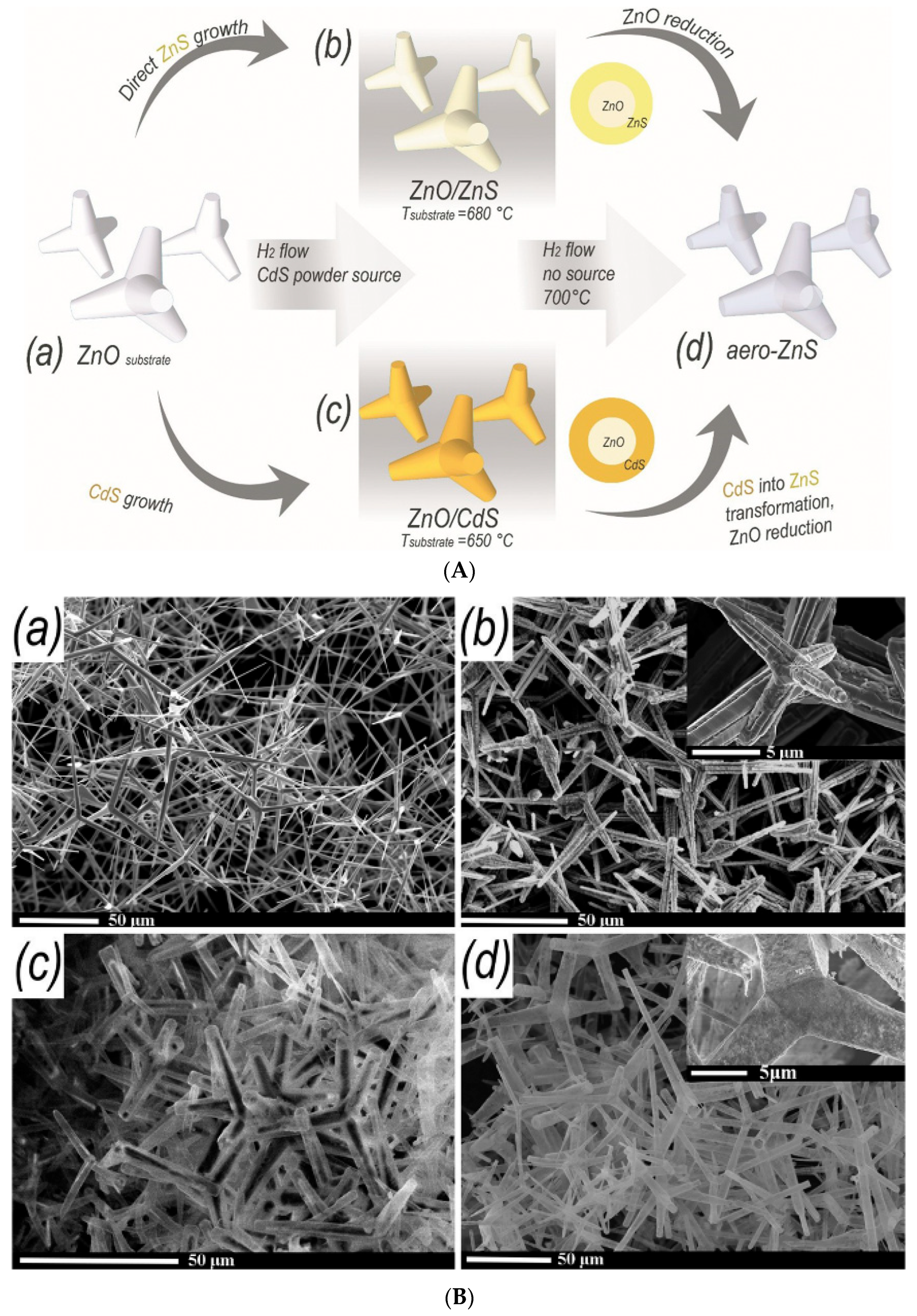
- Ursaki, V.; Braniste, T.; Zalamai, V.; Rusu, E.; Ciobanu, V.; Morari, V.; Podgornii, D.; Ricci, P.C.; Adelung, R.; Tiginyanu, I. Aero-ZnS prepared by physical vapor transport on three-dimensional networks of sacrificial ZnO microtetrapods. Beilstein J. Nanotechnol. 2024, 15, 490–499. [Google Scholar] [CrossRef]
- Plesco, I.; Braniste, T.; Wolff, N.; Gorceac, L.; Duppel, V.; Cinic, B.; Mishra, Y.K.; Sarua, A.; Adelung, R.; Kienle, L.; et al. Aero-ZnS architectures with dual hydrophilic–hydrophobic properties for microfluidic applications. APL Mater. 2020, 8, 061105. [Google Scholar] [CrossRef]
- El-Atab, N.; Nayfeh, A. 1D versus 3D quantum confinement in 1–5 nm ZnO nanoparticle agglomerations for application in charge-trapping memory devices. Nanotechnology 2016, 27, 275205. [Google Scholar] [CrossRef] [PubMed]
- Hewlett, R.M.; McLachlan, M.A. Surface Structure Modification of ZnO and the Impact on Electronic Properties. Adv. Mater. 2016, 28, 3893–3921. [Google Scholar] [CrossRef] [PubMed]
- Vanmaekelbergh, D.; van Vugt, L.K. ZnO nanowire lasers. Nanoscale 2011, 3, 2783–2800. [Google Scholar] [CrossRef] [PubMed]
- Zahoor, R.; Jalil, A.; Ilyas, S.Z.; Ahmed, S.; Hassan, A. Optoelectronic and solar cell applications of ZnO nanostructures. Results Surf. Interfaces 2021, 2, 100003. [Google Scholar] [CrossRef]
- Racca, L.; Canta, M.; Dumontel, B.; Ancona, A.; Limongi, T.; Garino, N.; Laurenti, M.; Canavese, G.; Cauda, V. 12—Zinc Oxide Nanostructures in Biomedicine. In Smart Nanoparticles for Biomedicine; Ciofani, G., Ed.; Elsevier: Amsterdam, The Netherlands, 2018; pp. 171–187. [Google Scholar] [CrossRef]
- Muruganandham, M.; Zhang, Y.; Suri, R.; Lee, G.-J.; Chen, P.-K.; Hsieh, S.-H.; Sillanpää, M.; Wu, J. Environmental Applications of ZnO Materials. J. Nanosci. Nanotechnol. 2015, 15, 6900–6913. [Google Scholar] [CrossRef]
- Sha, R.; Basak, A.; Maity, P.C.; Badhulika, S. ZnO nano-structured based devices for chemical and optical sensing applications. Sens. Actuators Rep. 2022, 4, 100098. [Google Scholar] [CrossRef]
- Liu, L.; Miao, X.; Cheng, X.; Wang, H.; Guo, M.; Cheng, F.; Zhang, M. Preparation and characterization of ZnO/SiO2@n-octadecane nanocapsule for ultraviolet absorbing and photothermal conversion energy storage. J. Energy Storage 2022, 54, 105363. [Google Scholar] [CrossRef]
- Xu, H.-Y.; Zhang, S.-Q.; Wang, Y.-F.; Xu, Y.; Dong, L.-M.; Komarneni, S. New insights into the photocatalytic mechanism of pristine ZnO nanocrystals: From experiments to DFT calculations. Appl. Surf. Sci. 2023, 614, 156225. [Google Scholar] [CrossRef]
- Hsu, N.-F.; Chung, T.-K.; Chang, M.; Chen, H.-J. Rapid Synthesis of Piezoelectric ZnO-Nanostructures for Micro Power-Generators. J. Mater. Sci. Technol. 2013, 29, 893–897. [Google Scholar] [CrossRef]
- Lee, J.-H.; Lee, G.-S.; Park, E.-N.; Jo, D.-H.; Kim, S.-W.; Lee, H.-C. Synthesis of Planar-Type ZnO Powder in Non-Nano Scale Dimension and Its Application in Ultraviolet Protection Cosmetics. Materials 2023, 16, 2099. [Google Scholar] [CrossRef]
- Amosov, A.P.; Novikov, V.A.; Kachkin, E.M.; Kryukov, N.A.; Titov, A.A.; Sosnin, I.M.; Merson, D.L. The Solution Combustion Synthesis of ZnO Powder for the Photodegradation of Phenol. Ceramics 2022, 5, 928–946. [Google Scholar] [CrossRef]
- Raha, S.; Ahmaruzzaman, M. ZnO nanostructured materials and their potential applications: Progress, challenges and perspectives. Nanoscale Adv. 2022, 4, 1868–1925. [Google Scholar] [CrossRef] [PubMed]
- Islam, F.; Shohag, S.; Uddin, M.J.; Islam, M.R.; Nafady, M.H.; Akter, A.; Mitra, S.; Roy, A.; Emran, T.B.; Cavalu, S. Exploring the Journey of Zinc Oxide Nanoparticles (ZnO-NPs) toward Biomedical Applications. Materials 2022, 15, 2160. [Google Scholar] [CrossRef]
- Paisrisarn, P.; Yasui, T.; Zhu, Z.; Klamchuen, A.; Kasamechonchung, P.; Wutikhun, T.; Yordsri, V.; Baba, Y. Tailoring ZnO nanowire crystallinity and morphology for label-free capturing of extracellular vesicles. Nanoscale 2022, 14, 4484–4494. [Google Scholar] [CrossRef]
- Li, F.; Meng, Y.; Kang, X.; Yip, S.; Bu, X.; Zhang, H.; Ho, J.C. High-mobility In and Ga co-doped ZnO nanowires for high-performance transistors and ultraviolet photodetectors. Nanoscale 2020, 12, 16153–16161. [Google Scholar] [CrossRef]
- Abubakar, S.; Ying Chyi, J.L.; Tan, S.T.; Sagadevan, S.; Talib, Z.A.; Paiman, S. Nanoscale domain imaging and the electromechanical response of zinc oxide nanorod arrays synthesized on different substrates. J. Mater. Res. Technol. 2021, 14, 2451–2463. [Google Scholar] [CrossRef]
- Bakry, M.; Ismail, W.; Abdelfatah, M.; El-Shaer, A. Low-cost fabrication methods of ZnO nanorods and their physical and photoelectrochemical properties for optoelectronic applications. Sci. Rep. 2024, 14, 23788. [Google Scholar] [CrossRef]
- Yi, C.; Yu, Z.; Ren, Q.; Liu, X.; Wang, Y.; Sun, X.; Yin, S.; Pan, J.; Huang, X. Nanoscale ZnO-based photosensitizers for photodynamic therapy. Photodiagnosis Photodyn. Ther. 2020, 30, 101694. [Google Scholar] [CrossRef]
- Wang, Y.; Coppel, Y.; Lepetit, C.; Marty, J.-D.; Mingotaud, C.; Kahn, M.L. Anisotropic growth of ZnO nanoparticles driven by the structure of amine surfactants: The role of surface dynamics in nanocrystal growth. Nanoscale Adv. 2021, 3, 6088–6099. [Google Scholar] [CrossRef]
- Brás, M.; Zanoni, J.; Falcão, B.P.; Leitão, J.P.; Costa, F.M.; Monteiro, T.; Pereira, S.O.; Rodrigues, J. Label-Free Nanoscale ZnO Tetrapod-Based Transducers for Tetracycline Detection. ACS Appl. Nano Mater. 2022, 5, 1232–1243. [Google Scholar] [CrossRef]
- Padmanaban, D.B.; Maguire, P.; Mariotti, D. Non-equilibrium defect chemistry in oxygen-rich zinc oxide nano-tetrapods synthesized using atmospheric pressure microplasma. J. Mater. Chem. A 2024, 12, 9212–9231. [Google Scholar] [CrossRef]
- Poschmann, M.P.M.; Siebert, L.; Lupan, C.; Lupan, O.; Schütt, F.; Adelung, R.; Stock, N. Surface Conversion of ZnO Tetrapods Produces Pinhole-Free ZIF-8 Layers for Selective and Sensitive H2 Sensing Even in Pure Methane. ACS Appl. Mater. Interfaces 2023, 15, 38674–38681. [Google Scholar] [CrossRef] [PubMed]
- Tseng, Y.-K.; Chuang, M.-H.; Chen, Y.-C.; Wu, C.-H. Synthesis of 1D, 2D, and 3D ZnO Polycrystalline Nanostructures Using the Sol-Gel Method. J. Nanotechnol. 2012, 2012, 712850. [Google Scholar] [CrossRef]
- Dmytruk, A.; Dmitruk, I.; Shynkarenko, Y.; Belosludov, R.; Kasuya, A. ZnO nested shell magic clusters as tetrapod nuclei. RSC Adv. 2017, 7, 21933–21942. [Google Scholar] [CrossRef]
- Zhang, X.-H.; Xie, S.-Y.; Jiang, Z.-Y.; Xie, Z.-X.; Huang, R.-B.; Zheng, L.-S.; Kang, J.-Y.; Sekiguchi, T. Microwave plasma growth and high spatial resolution cathodoluminescent spectrum of tetrapod ZnO nanostructures. J. Solid State Chem. 2003, 173, 109–113. [Google Scholar] [CrossRef]
- Tawale, J.S.; Dey, K.K.; Pasricha, R.; Sood, K.N.; Srivastava, A.K. Synthesis and characterization of ZnO tetrapods for optical and antibacterial applications. Thin Solid Film. 2010, 519, 1244–1247. [Google Scholar] [CrossRef]
- Norton, D.P.; Heo, Y.W.; Ivill, M.P.; Ip, K.; Pearton, S.J.; Chisholm, M.F.; Steiner, T. ZnO: Growth, doping & processing. Mater. Today 2004, 7, 34–40. [Google Scholar] [CrossRef]
- Chen, L.; Song, W.; Xie, C.; Lin, L.; Wang, J. A novel combustion method to prepare tetrapod nano-ZnO. Mater. Lett. 2007, 61, 4603–4605. [Google Scholar] [CrossRef]
- Rackauskas, S.; Klimova, O.; Jiang, H.; Nikitenko, A.; Chernenko, K.A.; Shandakov, S.D.; Kauppinen, E.I.; Tolochko, O.V.; Nasibulin, A.G. A Novel Method for Continuous Synthesis of ZnO Tetrapods. J. Phys. Chem. C 2015, 119, 16366–16373. [Google Scholar] [CrossRef]
- Zhao, Y.N.; Cao, M.S.; Jin, H.B.; Shi, X.L.; Li, X.; Agathopoulos, S. Combustion oxidization synthesis of unique cage-like nanotetrapod ZnO and its optical property. J. Nanosci. Nanotechnol. 2006, 6, 2525–2528. [Google Scholar] [CrossRef]
- Zahran, H.; Yahia, I.S. Synthesis and characterization of ZnO tetrapods. Appl. Phys. A 2015, 119, 1397–1403. [Google Scholar] [CrossRef]
- Lin, H.-F.; Liao, S.-C.; Hu, C.-T. A new approach to synthesize ZnO tetrapod-like nanoparticles with DC thermal plasma technique. J. Cryst. Growth 2009, 311, 1378–1384. [Google Scholar] [CrossRef]
- Chiu, W.-H.; Lee, C.-H.; Cheng, H.-M.; Lin, H.-F.; Liao, S.-C.; Wu, J.-M.; Hsieh, W.-F. Efficient electron transport in tetrapod-like ZnO metal-free dye-sensitized solar cells. Energy Environ. Sci. 2009, 2, 694–698. [Google Scholar] [CrossRef]
- Lee, C.-H.; Chiu, W.-H.; Lee, K.-M.; Yen, W.-H.; Lin, H.-F.; Hsieh, W.-F.; Wu, J.-M. The influence of tetrapod-like ZnO morphology and electrolytes on energy conversion efficiency of dye-sensitized solar cells. Electrochim. Acta 2010, 55, 8422–8429. [Google Scholar] [CrossRef]
- Lin, H.-F.; Liao, S.-C.; Hung, S.-W. The dc thermal plasma synthesis of ZnO nanoparticles for visible-light photocatalyst. J. Photochem. Photobiol. A Chem. 2005, 174, 82–87. [Google Scholar] [CrossRef]
- Afify, A.; Elsayed, A.; Khadra, A.; Hassan, M.; Ataalla, M.; Mohamed, A.; Tulliani, J.-M. The Sensing Characteristics of ZnO Tetrapods Synthesized by Microwave Evaporation. J. Commun. Softw. Syst. 2018, 14, 4–8. [Google Scholar] [CrossRef]
- Chamoli, P.; Shukla, R.K.; Bezbaruah, A.N.; Kar, K.K.; Raina, K.K. Microwave-assisted rapid synthesis of honeycomb core-ZnO tetrapods nanocomposites for excellent photocatalytic activity against different organic dyes. Appl. Surf. Sci. 2021, 555, 149663. [Google Scholar] [CrossRef]
- Seok, E.; Yang, J.-Y.; Han, H.-H.; Jeong, G.-H. Facile Fabrication of Flexible Photosensors Using Zinc Oxide Tetrapods and Their Ultraviolet Response Evaluation. Appl. Sci. Converg. Technol. 2023, 32, 168–171. [Google Scholar] [CrossRef]
- Abidov, A.; Kim, S.; Kim, Y.B. Rapid Fabrication of ZnO Tetrapod Based Photoconductive Cell by Microwave Synthesis Technology. Sci. Adv. Mater. 2016, 8, 652–656. [Google Scholar] [CrossRef]
- Alsultany, F.H.; Hassan, Z.; Ahmed, N.M. Large-scale uniform ZnO tetrapods on catalyst free glass substrate by thermal evaporation method. Mater. Res. Bull. 2016, 79, 63–68. [Google Scholar] [CrossRef]
- Zanotti, L.; Calestani, D.; Villani, M.; Zha, M.; Zappettini, A.; Paorici, C. Vapour-phase growth, purification and large-area deposition of ZnO tetrapod nanostructures. Cryst. Res. Technol. 2010, 45, 667–671. [Google Scholar] [CrossRef]
- Yang, D.; Gopal, R.A.; Lkhagvaa, T.; Choi, D. Oxidizing agent impacting on growth of ZnO tetrapod nanostructures and its characterization. Environ. Res. 2021, 197, 111032. [Google Scholar] [CrossRef] [PubMed]
- Bhoomanee, C.; Hongsith, N.; Wongrat, E.; Choopun, S.; Wongratanaphisan, D. Effect of Solution on Growth of Zinc Oxide Tetrapod by Thermal Oxidation Technique. Chiang Mai J. Sci. 2011, 38, 187–192. [Google Scholar]
- Aziz, B.; Majid, A.; ghani, l.; Aziz, I. Photoluminescence effect on phosphorous irradiated zinc oxide (ZnO) nanotetrapods synthesized by simple thermal oxidation method. J. Phys. Its Appl. 2020, 3, 107–112. [Google Scholar] [CrossRef]
- Hongsith, N.; Chairuangsri, T.; Phaechamud, T.; Choopun, S. Growth kinetic and characterization of tetrapod ZnO nanostructures. Solid State Commun. 2009, 149, 1184–1187. [Google Scholar] [CrossRef]
- Mishra, Y.K.; Modi, G.; Cretu, V.; Postica, V.; Lupan, O.; Reimer, T.; Paulowicz, I.; Hrkac, V.; Benecke, W.; Kienle, L.; et al. Direct Growth of Freestanding ZnO Tetrapod Networks for Multifunctional Applications in Photocatalysis, UV Photodetection, and Gas Sensing. ACS Appl. Mater. Interfaces 2015, 7, 14303–14316. [Google Scholar] [CrossRef]
- Antoine, T.E.; Mishra, Y.K.; Trigilio, J.; Tiwari, V.; Adelung, R.; Shukla, D. Prophylactic, therapeutic and neutralizing effects of zinc oxide tetrapod structures against herpes simplex virus type-2 infection. Antivir. Res. 2012, 96, 363–375. [Google Scholar] [CrossRef]
- Martinez, W.M.; Spear, P.G. Amino acid substitutions in the V domain of nectin-1 (HveC) that impair entry activity for herpes simplex virus types 1 and 2 but not for Pseudorabies virus or bovine herpesvirus 1. J. Virol. 2002, 76, 7255–7262. [Google Scholar] [CrossRef]
- Calestani, D.; Zha, M.; Mosca, R.; Zappettini, A.; Carotta, M.C.; Di Natale, V.; Zanotti, L. Growth of ZnO tetrapods for nanostructure-based gas sensors. Sens. Actuators B Chem. 2010, 144, 472–478. [Google Scholar] [CrossRef]
- He, F.-Q.; Zhao, Y.-P. Growth and optical properties of peculiar ZnO tetrapods. J. Phys. D Appl. Phys. 2006, 39, 2105–2108. [Google Scholar] [CrossRef]
- Yan, Y.; Zhou, L.; Zou, J.; Zhang, Y. Synthesis and growth discussion of novel ZnO nanotetrapods with pearl-necklace-shaped arms. Appl. Phys. A 2009, 94, 559–565. [Google Scholar] [CrossRef]
- Wang, B.-B.; Xie, J.-J.; Yuan, Q.; Zhao, Y.-P. Growth mechanism and joint structure of ZnO tetrapods. J. Phys. D Appl. Phys. 2008, 41, 102005. [Google Scholar] [CrossRef]
- Lyapina, O.; Baranov, A.; Knotko, A.; Kononenko, O. Synthesis of ZnO nanotetrapods. Inorg. Mater. 2008, 44, 846–852. [Google Scholar] [CrossRef]
- Mecklenburg, M.; Schuchardt, A.; Mishra, Y.; Kaps, S.; Adelung, R.; Lotnyk, A.; Kienle, L.; Karl, S. Aerographite: Ultra Lightweight, Flexible Nanowall, Carbon Microtube Material with Outstanding Mechanical Performance (Adv. Mater. 26/2012). Adv. Mater. 2012, 24, 3437. [Google Scholar] [CrossRef]
- Li, X.; Liu, Y.; Song, X.; Wang, H.; Gu, H.; Zeng, H. Intercrossed Carbon Nanorings with Pure Surface States as Low-Cost and Environment-Friendly Phosphors for White-Light-Emitting Diodes. Angew. Chem. Int. Ed. 2015, 54, 1759–1764. [Google Scholar] [CrossRef]
- Geim, A.K.; Novoselov, K.S. The rise of graphene. Nat. Mater. 2007, 6, 183–191. [Google Scholar] [CrossRef]
- He, Y.; Chen, W.; Li, X.; Zhang, Z.; Fu, J.; Zhao, C.; Xie, E. Freestanding Three-Dimensional Graphene/MnO2 Composite Networks As Ultralight and Flexible Supercapacitor Electrodes. ACS Nano 2013, 7, 174–182. [Google Scholar] [CrossRef]
- Baek, H.; Lee, C.-H.; Chung, K.; Yi, G.-C. Epitaxial GaN Microdisk Lasers Grown on Graphene Microdots. Nano Lett. 2013, 13, 2782–2785. [Google Scholar] [CrossRef]
- Yang, R.; Zhang, Y.; Li, J.; Han, Q.; Zhang, W.; Lu, C.; Yang, Y.; Dong, H.; Wang, C. Graphene oxide assisted synthesis of GaN nanostructures for reducing cell adhesion. Nanoscale 2013, 5, 11019–11027. [Google Scholar] [CrossRef]
- Han, W.; Zettl, A. An Efficient Route to Graphitic Carbon-Layer-Coated Gallium Nitride Nanorods. Adv. Mater. 2002, 14, 1560–1562. [Google Scholar] [CrossRef]
- Parlak, O.; Kumar Mishra, Y.; Grigoriev, A.; Mecklenburg, M.; Luo, W.; Keene, S.; Salleo, A.; Schulte, K.; Ahuja, R.; Adelung, R.; et al. Hierarchical Aerographite nano-microtubular tetrapodal networks based electrodes as lightweight supercapacitor. Nano Energy 2017, 34, 570–577. [Google Scholar] [CrossRef]
- Gong, W.; Chen, W.; He, J.; Tong, Y.; Liu, C.; Su, L.; Gao, B.; Yang, H.; Zhang, Y.; Zhang, X. Substrate-independent and large-area synthesis of carbon nanotube thin films using ZnO nanorods as template and dopamine as carbon precursor. Carbon 2015, 83, 275–281. [Google Scholar] [CrossRef]
- Ding, L.X.; Li, G.R.; Wang, Z.L.; Liu, Z.Q.; Liu, H.; Tong, Y.X. Porous Ni@Pt core-shell nanotube array electrocatalyst with high activity and stability for methanol oxidation. Chem. (Weinh. Der Bergstr. Ger.) 2012, 18, 8386–8391. [Google Scholar] [CrossRef] [PubMed]
- Zhao, Y.; Jiang, P.; Xie, S.-S. ZnO-template-mediated synthesis of three-dimensional coral-like MnO2 nanostructure for supercapacitors. J. Power Sources 2013, 239, 393–398. [Google Scholar] [CrossRef]
- Wang, Z.-L.; Guo, R.; Ding, L.-X.; Tong, Y.-X.; Li, G.-R. Controllable Template-Assisted Electrodeposition of Single- and Multi-Walled Nanotube Arrays for Electrochemical Energy Storage. Sci. Rep. 2013, 3, 1204. [Google Scholar] [CrossRef]
- Plesco, I.; Strobel, J.; Schütt, F.; Himcinschi, C.; Ben Sedrine, N.; Monteiro, T.; Correia, M.R.; Gorceac, L.; Cinic, B.; Ursaki, V.; et al. Hierarchical Aerographite 3D flexible networks hybridized by InP micro/nanostructures for strain sensor applications. Sci. Rep. 2018, 8, 13880. [Google Scholar] [CrossRef]
- Rasch, F.; Schütt, F.; Saure, L.M.; Kaps, S.; Strobel, J.; Polonskyi, O.; Nia, A.S.; Lohe, M.R.; Mishra, Y.K.; Faupel, F.; et al. Wet-Chemical Assembly of 2D Nanomaterials into Lightweight, Microtube-Shaped, and Macroscopic 3D Networks. ACS Appl. Mater. Interfaces 2019, 11, 44652–44663. [Google Scholar] [CrossRef]
- Braniste, T.; Ciobanu, V.; Schütt, F.; Mimura, H.; Raevschi, S.; Adelung, R.; Pugno, N.M.; Tiginyanu, I. Self-Propelled Aero-GaN Based Liquid Marbles Exhibiting Pulsed Rotation on the Water Surface. Materials 2021, 14, 5086. [Google Scholar] [CrossRef]


| Type of Material | Synthesis Method | Application | References |
|---|---|---|---|
| Aerographite | Chemical vapor deposition (CVD) | Optoelectronic technologies, ultra-lightweight, electrically conductive, electrode material/supercapacitor | [20,21,22,23] |
| Aerographite-GaN | Hybrid vapor-phase epitaxy (HVPE) | Electronic, photonic, and sensor applications | [24] |
| Aero-β-Ga2O3/ZnGa2O4 nanocomposite | HVPE | Electrochemical application | [25] |
| Aero-Ga2O3 | HVPE | Photocatalytic Water purification | [26] |
| Aero-GaN | HVPE | Ultra-lightweight pressure sensor/portable electrical equipment | [27,28] |
| Aero-TiO2 | Atomic layer deposition (ALD) | Photocatalytic degradation of drugs (tetracycline) Photocatalytic applications | [29,30] |
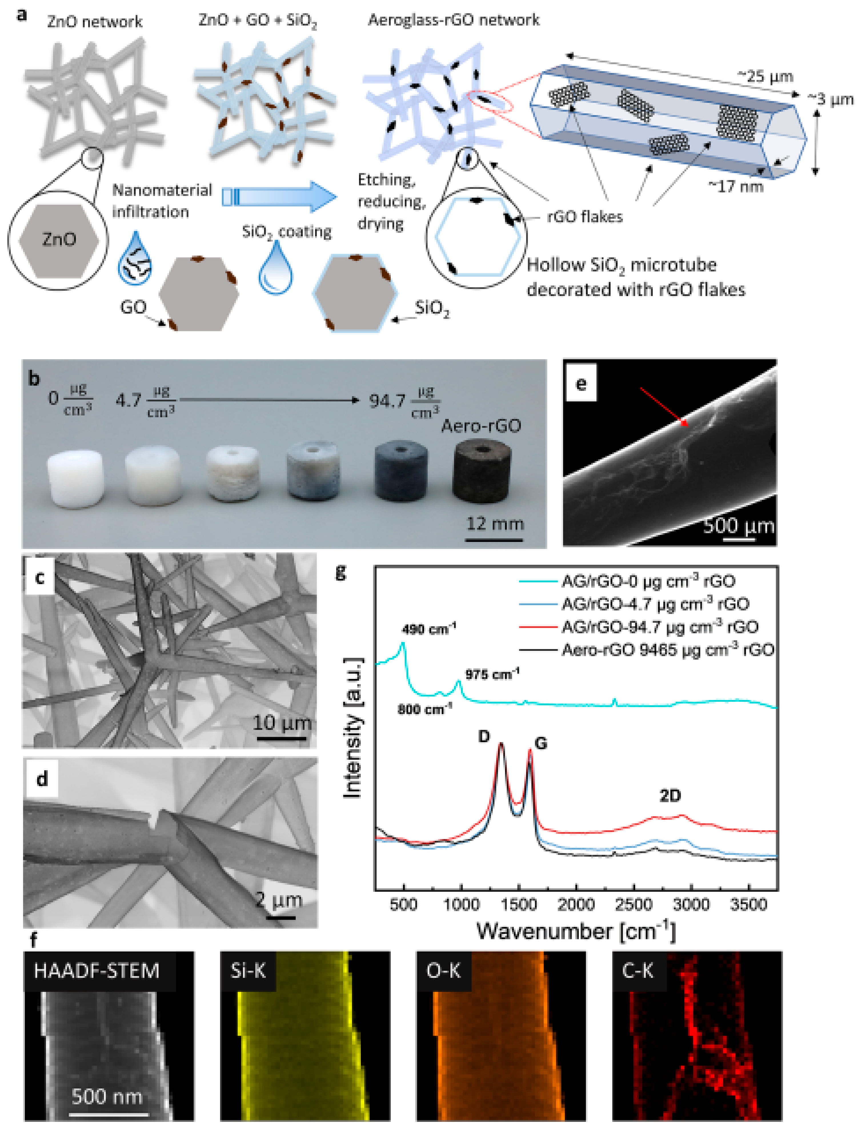
| Hybrid Aero-SiO2/rGO | Wet-chemical coating | Enhanced and rapid volumetric photothermal response | [31] |
| Aero-ZnS | HVPE | Micro-fluidic applications | [32,33] |
Disclaimer/Publisher’s Note: The statements, opinions and data contained in all publications are solely those of the individual author(s) and contributor(s) and not of MDPI and/or the editor(s). MDPI and/or the editor(s) disclaim responsibility for any injury to people or property resulting from any ideas, methods, instructions or products referred to in the content. |
© 2025 by the authors. Licensee MDPI, Basel, Switzerland. This article is an open access article distributed under the terms and conditions of the Creative Commons Attribution (CC BY) license (https://creativecommons.org/licenses/by/4.0/).
Share and Cite
Orha, C.; Nicolaescu, M.; Morariu, M.-I.; Galatonova, T.; Busuioc, S.; Lazau, C.; Bandas, C. A Comprehensive Review on Aero-Materials: Present and Future Perspectives. Coatings 2025, 15, 754. https://doi.org/10.3390/coatings15070754
Orha C, Nicolaescu M, Morariu M-I, Galatonova T, Busuioc S, Lazau C, Bandas C. A Comprehensive Review on Aero-Materials: Present and Future Perspectives. Coatings. 2025; 15(7):754. https://doi.org/10.3390/coatings15070754
Chicago/Turabian StyleOrha, Corina, Mircea Nicolaescu, Mina-Ionela Morariu (Popescu), Tatiana Galatonova, Simon Busuioc, Carmen Lazau, and Cornelia Bandas. 2025. "A Comprehensive Review on Aero-Materials: Present and Future Perspectives" Coatings 15, no. 7: 754. https://doi.org/10.3390/coatings15070754
APA StyleOrha, C., Nicolaescu, M., Morariu, M.-I., Galatonova, T., Busuioc, S., Lazau, C., & Bandas, C. (2025). A Comprehensive Review on Aero-Materials: Present and Future Perspectives. Coatings, 15(7), 754. https://doi.org/10.3390/coatings15070754