Article

Ultra-Thin Films of CdS Doped with Silver: Synthesis and Modification of Optical, Structural, and Morphological Properties by the Doping Concentration Effect

by
Juan P. Molina-Jiménez
1,
Sindi D. Horta-Piñeres
1,*,
S. J. Castillo
2,
J. L. Izquierdo
3 and
D. A. Avila
1
1
Laboratorio de Óptica e Informática, Universidad Popular del Cesar, Valledupar 200001, Cesar, Colombia
2
Departamento de Investigación en Física, Universidad de Sonora, Hermosillo 83190, Sonora, Mexico
3
Grupo de Investigación e Innovación en Energía GIIEN, Institución Universitaria Pascual Bravo, Medellín 050001, Antioquia, Colombia
*
Author to whom correspondence should be addressed.
Coatings 2025, 15(4), 431; https://doi.org/10.3390/coatings15040431
Submission received: 20 December 2024 / Revised: 25 February 2025 / Accepted: 1 March 2025 / Published: 7 April 2025
(This article belongs to the Special Issue Thin-Film Synthesis, Characterization and Properties)

Abstract

:
Obtaining wide energy-gap semiconductor ultra-thin films is an important aspect for their application in sulfide-based solar cells. By reducing the optical losses associated with light reflection and exhibiting absorption edge shifts towards short wavelengths, these layers can optimize the amount of photons interacting with the active photovoltaic material, which increases the conversion efficiency of the solar cell. Ultra-thin CdS films were prepared by a low-cost chemical synthesis and the impact of silver doping on the optical, structural, and morphological properties was evaluated. SEM micrographs revealed that the layers are ultra-thin, homogeneous and uniform, with a reduction in particle size with increasing doping concentration. X-ray diffraction data confirmed the crystallization of CdS in the hexagonal phase for all prepared samples. A low concentration contributed to the formation of Ag2S in the monoclinic phase according to the diffractograms. The optical properties of the thin films revealed an absorption edge shift that increased the CdS band gap from 2.267 ± 0.007 to 2.353 ± 0.005 eV with increasing doping concentration, improving the spectral transmittance response. These results make these layers particularly useful for implementation in next-generation flexible photovoltaic devices.

1. Introduction

The search for high-performance semiconductor materials for efficient solar energy conversion remains a fundamental challenge in flexible solar cell research [1]. Recent research highlights significant progress in photovoltaic technology, particularly through the use of bio-nano materials in dye-sensitized solar cells (DSSCs), achieving light-to-power conversion efficiencies of up to 11% [2]. Additionally, advancements in perovskite, tandem, and organic solar cells have improved efficiency, stability, and scalability [3]. Silicon nanostructures also show promise for enhancing solar energy systems [4].
Cadmium sulfide (CdS) has been a material of great interest for this application, mainly because of its wide energy gap located in the visible spectral range (2.42 eV in bulk). In its nanostructured scale, it has presented a direct range absorption coefficient, high percentages of spectral transmittance, photoconductivity in the visible region, electronic affinity, n-type electrical conductivity, low resistivity and good ohmic contact [5,6,7]. Therefore, it has been implemented as an n-type layer in heterojunction-type solar cells, particularly a CdS/CdTe structure, demonstrating a high power conversion rate with projected theoretical efficiencies up to 28–30% [8]. However, one of the critical obstacles for the large-scale production of this type of heterostructures has been the low reproducibility of techniques that guarantee the obtaining of ultra-thin films, high homogeneity and uniformity in the coatings, which are essential characteristics to ensure an efficient transport of the charge carriers and minimize energy losses; in addition, these films must maintain excellent crystalline quality and high percentages of optical transmission, in the case of the window layer. This optical material has also been noted for its excellent photoluminescent properties and high crystalline quality, which has made it an ideal material for applications in advanced optoelectronic devices such as lasers and light detectors [9]. A relevant example is the study on the liquid-phase epitaxy of CdS, which demonstrates its potential in the fabrication of high-efficiency lasers and sensitive light detectors [4]. These advances highlight the importance of high-quality optical materials in the development of next-generation photonic technologies.
It is known that the optical, structural, morphological and electrical properties depend significantly on the fabrication technique used. Techniques such as chemical vapor deposition (CVD) [9], chemical vapor deposition of organometallic vapor (MOCVD) [10], spray pyrolysis (SP) [11] and sputtering [12] have been implemented, which demonstrate good quality thin films for implementation in solar cells. However, the physical instrumentation and the high cost of these techniques remain a major drawback to reproducibility.
Other physicochemical parameters involved in the synthesis processes, such as temperature [13], pH [14], reaction time [15], and the concentration of complexing agents and precursors [16], have been shown to exert a significant influence on the physical properties of thin films. Similarly, impurification of the host material through extrinsic doping has been relevant to the controlled modification of these properties [17,18,19,20].
The doping process, especially with metals such as silver (Ag), has the potential to improve these properties, but the incorporation of impurities through a single controlled synthesis process remains an extremely complex task. In addition, the ability to precisely control the synthesis parameters, such as temperature, dopant concentration and reaction kinetics, without compromising the structural and morphological quality of the films, is a critical skill that has not yet been fully mastered.
Some reported investigations, for example, Taur et al., have examined the influence of thermal annealing on the optoelectronic and physicochemical properties of CdS:Ag thin films. It was found that the band gap decreased from 2.28 to 2.14 eV, and the I-V response of the thin films revealed an adequate photo-sensitivity result of 72% to 96% after illumination with a light source of 100 mW/cm2 [21]. Ferrá-Gonzalez et al. found that the band-gap energy and roughness of CdS:Ag thin films increase slightly with silver concentration up to a point where cadmium is depleted and is no longer replaced, at which point silver sulfide (Ag2S) begins to form. The band gap and roughness of the films now start to decrease with increasing AgNO3 concentration, classifying these films for optoelectronic applications such as TFTs [22]. Pacheco et al. studied the changes in the photoluminescence properties of CdS thin films due to the effect of Ag+ doping. They were able to show that Ag+ doping had an impact on quantum confinement, generating higher energy emissions as the particle size decreased from 5.46 to 4.12 nm [23].
Although recent studies have explored the effect of silver doping concentration on CdS films by different deposition techniques, there are actually few reports that implement a chemical synthesis and incorporate the dopant in the same synthesis process in order to ensure reproducibility in obtaining thin films. Najm et al., recently reported the fabrication of CBD-deposited CdS thin films, explaining in detail the formation mechanism and the effect of Ag doping concentration on the optical, structural, morphological and electrical properties. The doping was carried out in a single process and the synthesized films presented low optical absorption percentages with increasing Ag concentration; however, the band gap was reduced with respect to the pure CdS thin film, due to the concentration effect. The doping with Ag had a great impact on the morphology of the CdS film, since according to the SEM images the CdS granular structures were randomly distributed along the substrate and no uniformity was evidenced, tending to agglomerate with each other to form clusters with many voids due to the lack of reactivity [24], limiting their applicability in photovoltaic devices. As research in semiconductor materials for solar cells advances, alternative technologies such as thin films based on colloidal cadmium quantum dots and lead chalcogenides, which offer tunable electronic and optical properties by controlling the particle size, are emerging [25,26]. These technologies have been widely explored in photovoltaic devices, but face challenges related to stability and scalability, especially in flexible applications.
In contrast, CdS thin films remain a competitive option and present significant challenges related to obtaining ultra-thin films with high homogeneity, crystalline quality and relevant optical properties. The present investigation presents a complementary and detailed experimental approach for the optimization of the properties of CdS thin films by extrinsic doping with Ag. The comprehensive analysis of the synthesis parameters developed here and the controlled incorporation of the Ag dopant in a single chemical process not only provides a route towards the improvement of the optical, structural and morphological properties of CdS, in addition, provides a reproducible, scalable, low-cost and fast-access framework for obtaining nanostructures applied to high-efficiency flexible systems such as heterojunction solar cells.

2. Materials and Methods

2.1. Preparation of CdS:Ag Thin Films

Silver-doped cadmium sulfide (CdS:Ag) thin films were prepared by bath chemical synthesis. Table 1 describes the analytical grade precursor materials used for the synthesis of the CdS and CdS:Ag thin films.
The schematic diagram of the synthesis is shown in Figure 1. This physical system consists mainly of a beaker containing the precursor solution or chemical bath, a heating plate, a thermometer, and the 76 mm × 25 mm × 1 mm ZIBOJECT glass substrates, previously washed and sterilized with deionized water (DIW).
In the order shown in Figure 1, 10 mL of CdCl2 at 0.05 M, 20 mL of Na3C6H5O7 at 0.5M, 5 mL of KOH at 0.3 M, 5 mL of buffer solution at pH 10, 10 mL of CS(NH)2 at 0.5 M and 40 mL of DIW were added sequentially to the beaker as indicated by the numbering of the pipettes in Figure 1. In this way, the precursor solution for the synthesis of pristine CdS thin films was obtained. To obtain the Ag-doped CdS films at 0.25 mM, 0.5 mM and 1 mM, after the addition of thiourea, 5 mL solutions of AgNO3 were added separately to the bath at these concentrations. This doping process was carried out “in dark” to avoid precipitating the reaction. Subsequently, the substrates were immersed vertically into the beaker and kept in a thermal bath. The temperature was maintained at 60.0 ± 0.1 °C for 15.0 ± 0.1 min for all prepared samples. At the end of the deposition time, the substrates were removed from the reactor and immediately rinsed with DIW and air-dried.
To evaluate the reproducibility of this technique, multiple samples were synthesized under identical conditions in different weeks. The results, including mainly optical characterizations, showed minimal batch-to-batch variation, demonstrating the reliability of the technique. The synthesis parameters reported in the present investigation, such as molar concentrations of precursors, sequential order of synthesis, temperature, reaction time, pH, “in dark” treatment, position and type of substrate and doping concentrations, are the result of the optimization of multiple experimental trials, which will allow interested researchers to replicate the production of these nanostructures.

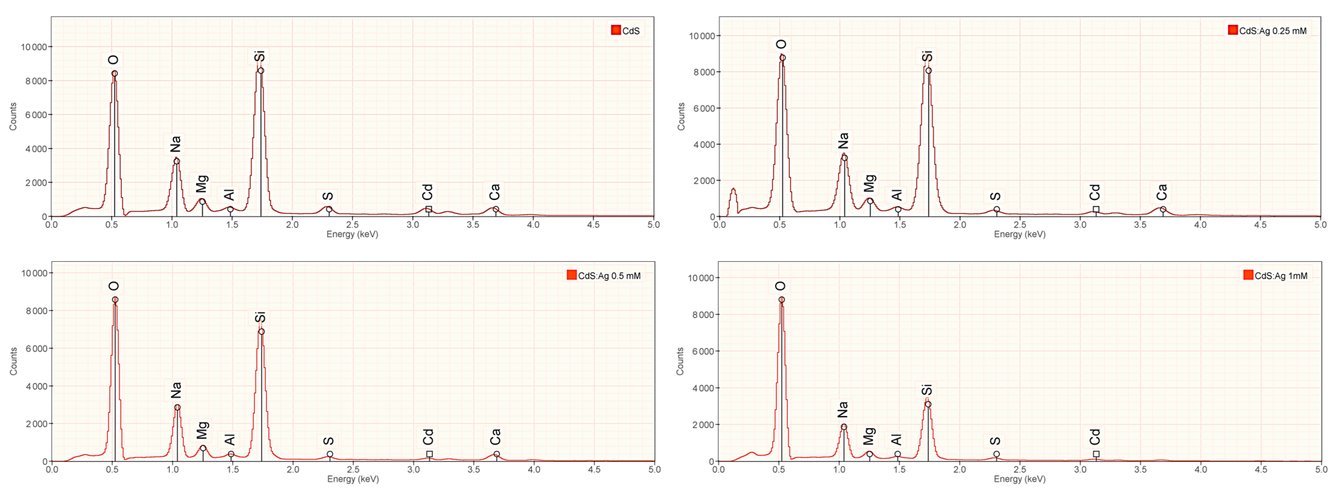
2.2. Characterization of CdS:Ag Thin Films

Structural characterization of CdS:Ag thin films was performed through X-ray diffraction analysis (XDR). An XPert PANalytical Empyrean Series II—Alpha1 X-ray diffractometer (XRD) XPert PANalytical Empyrean Series II—Alpha1 featuring CuKα radiation (λ = 1.5406 Å) was used for the identification of the crystalline phase and crystallite size of the samples. The peaks revealed in the diffractograms were indexed according to the PDF-2 database. The average crystallite size (D) was calculated as a function of the full width at half maximum intensity (FWHM) of the main reflections by applying Debye–Scherrer’s formula [6,27]:
D = 0.9 λ β cos θ
where λ is the incident X-ray wavelength, β is the full width at half peak diffraction maximum (FWHM) and θ is the Bragg angle.
The vibrational characteristics of the thin films were analyzed through the Raman spectroscopy technique using a Thermo Scientific DXR2 equipment (ThermoFisher SCIENTIFIC, Waltham, MA, USA) of the Raman Instruments line. A 532 nm laser with a power of 5.0 mW was used, and the spectrograph aperture was set to 50 µm.
The morphological and compositional characteristics were analyzed by SEM micrographs using a Helios 5 PFIB CXe scanning electron microscope (ThermoFisher SCIENTIFIC, Waltham, MA, USA). The main instrument of the microscope includes an Elstar Electron column with UC+ technology Resolution 0.6 nm, 2–20 keV, a Retractable STEM 3+ detector in the sample chamber with Resolution 0.6 nm at 30 kV and an integrated Pathfinder Alpine broad spectrum energy dispersive X-ray (EDS) system.
The optical spectral response was analyzed at room temperature using an ASEQ Instruments UV-Vis spectrometer (ASEQ Instruments, Vancouver, Canada) with a spectral resolution of 0.2 nm and an operating range of 200–1000 nm. The optical band gap was determined from the diffuse absorbance measurements through the following correlation [16,28]:
( α h υ ) 1 / n = A ( h υ E g )
where α is the absorption coefficient, h is Planck’s constant, υ is the frequency of the incident photon, A is a proportionality constant. Eg is the characteristic band gap of the material and the parameter n indicates the nature of the transition, where n = 2 for direct allowed transitions. Other experimental methods, such as photocurrent measurements, are particularly important in determining the characteristic band gap [29]. In this work, the optical band gap is investigated according to Tauc’s model, which uses Equation (2) to calculate the value of Eg from a linear extrapolation of ( α h υ ) 2 Vs photon energy ( h υ ) at the absorption limit; that is, when α 0 .
The extinction coefficient (k) as a function of wavelength (λ), was calculated from the following correlation [30,31]:
k = λ 4 π α
where α is the absorption coefficient.
For normal incidence, the reflectance affecting the radiation intensity is given by [31,32]:
R = ( n 1 ) 2 + k 2 ( n + 1 ) 2 + k 2
from Equation (4), we can obtain an expression for the refractive index (n):
n = 1 + R 1 R + 4 R ( 1 R ) 2 k 2
where R corresponds to the diffuse reflectance measurements and k corresponds to the extinction coefficient.
The real and imaginary components of the dielectric constant designated as ε′ and ε″, respectively, were calculated from the following relations [30,31,32,33]:
ε = n 2 k 2
ε = 2 n k
where n corresponds to the refractive index and k is the extinction coefficient.

3. Results and Discussion

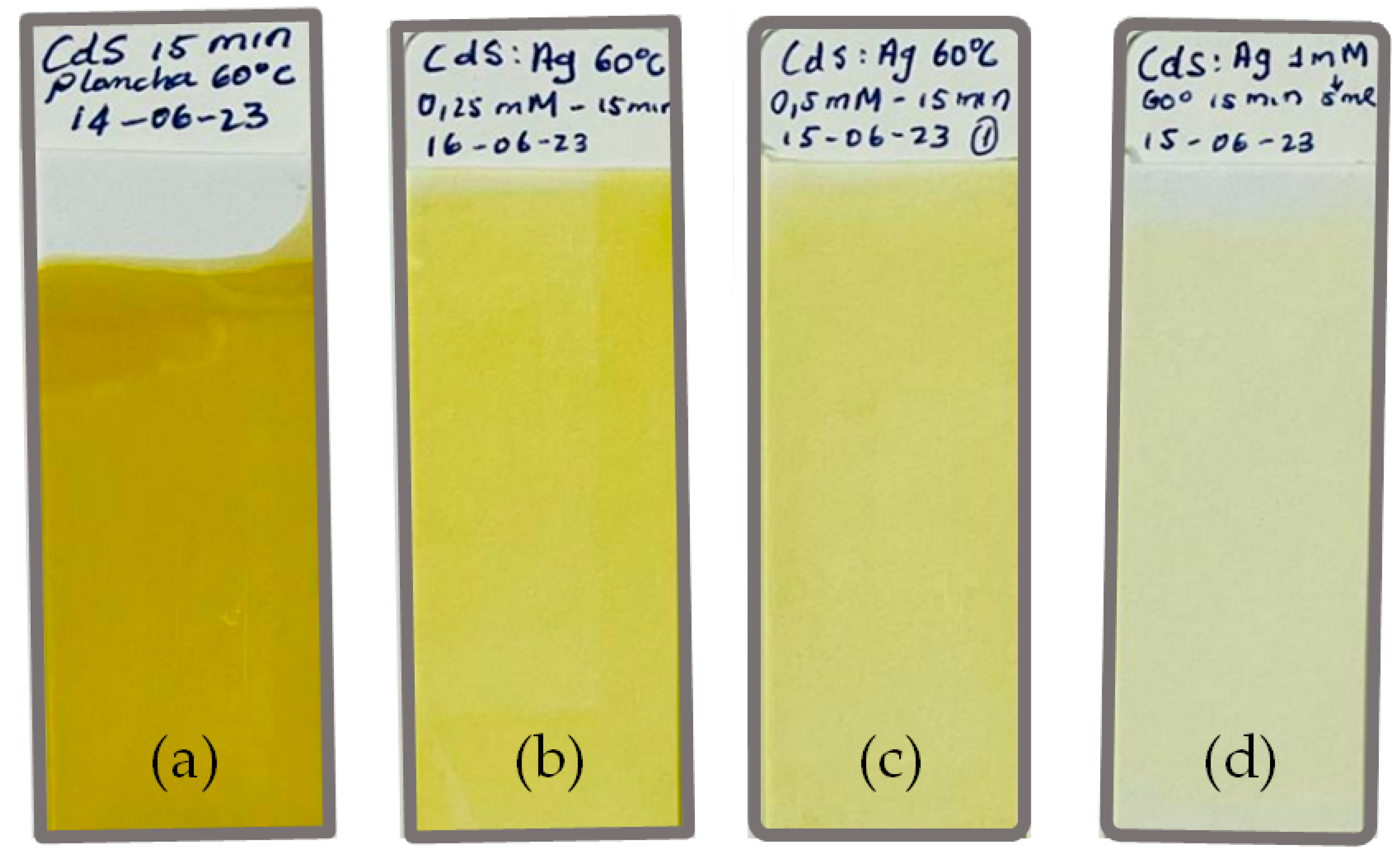
3.1. CdS Thin Films Deposited with Different Ag Doping Ratios

Figure 2 shows the actual images of thin films of (a) pristine CdS, (b) CdS:Ag 0.25 mM, (c) CdS:Ag 0.5 mM and (d) CdS:Ag 1 mM deposited by bath chemical synthesis.
Figure 2 shows that the thin films have a characteristic translucent yellow coloration in CdS, and this coloration tends to reduce as the molar concentration of Ag increases. The coatings present an important degree of homogeneity visibly, and are correctly adhered to the substrate.

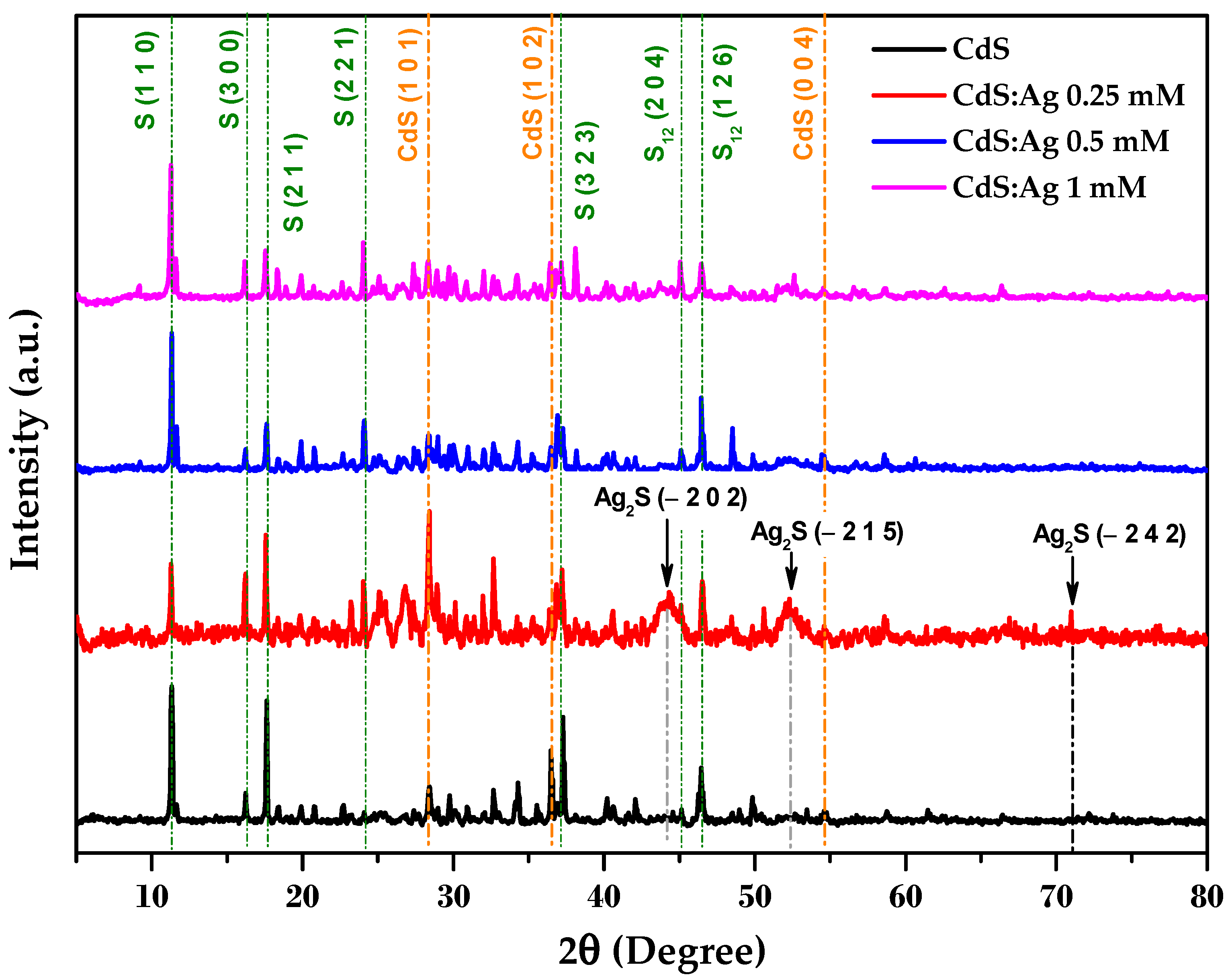
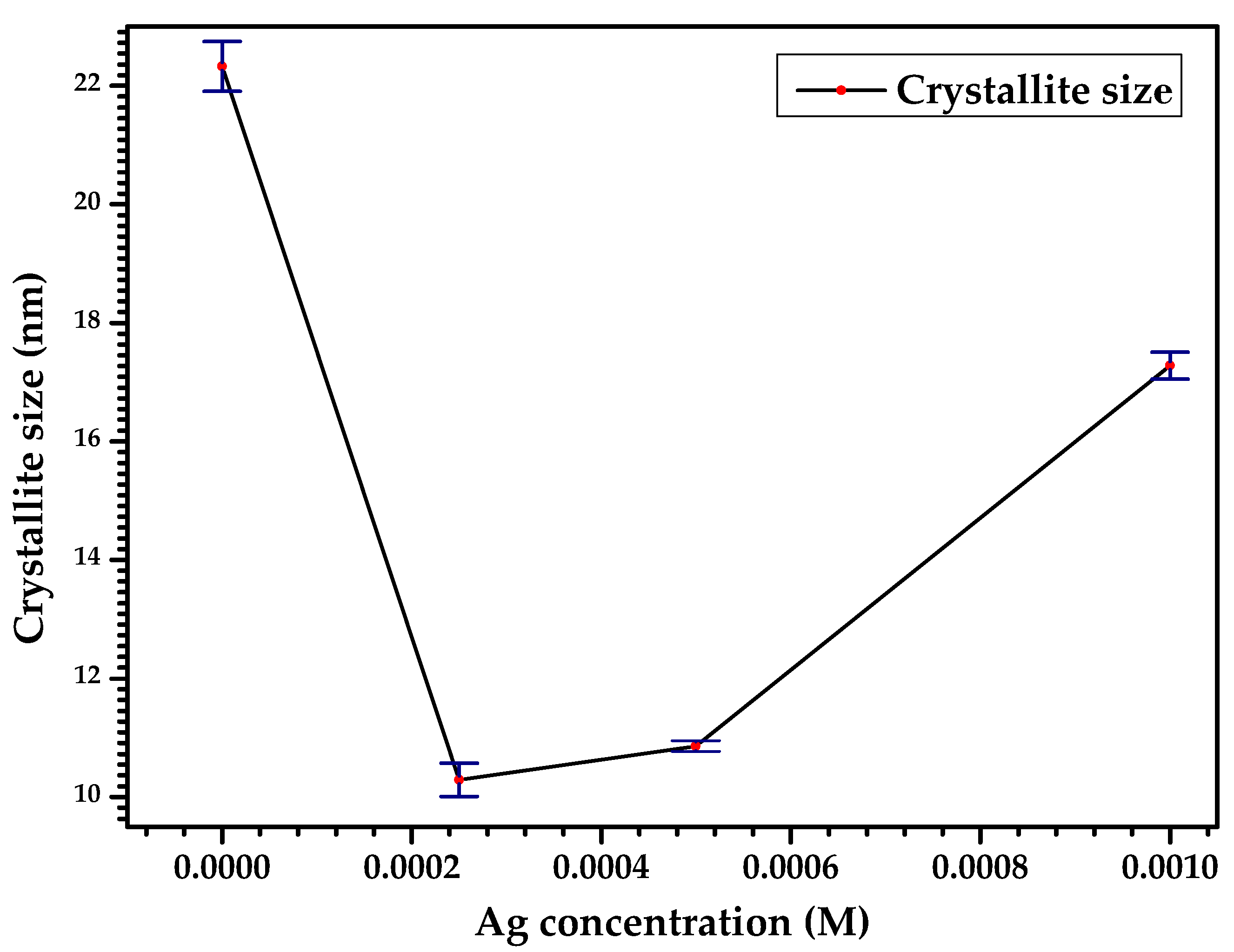
3.2. Structural Analysis

The incidence of doping on the crystallization of Ag-doped CdS and CdS thin films is examined by X-ray diffraction technique. Figure 3 exhibits the XDR patterns of CdS and CdS:Ag thin films for a 2θ diffraction angle varying from 5° to 80°. The presence of multiple peaks in the XDR pattern indicates that the thin films are polycrystalline in nature, and consist of fine and coarse grains. The diffraction peaks of all samples are found to agree well with the standard ICDD card (# 041-1049) of the hexagonal (wurtzite) structure of CdS with space group (P63mc). The peaks indexed to the (1 0 1), (1 0 2) and (0 0 4) planes correspond to this card, confirming the crystallization of CdS in all samples. In all XDR patterns, intense peaks are also observed at 2 θ = 11.15 ° , 16.39 ° , 17.78 ° , 24.39 ° and 37.16 ° , corresponding to the monoclinic phase of sulfur (S) according to ICDD card (# 76-0183), with other peaks located at 2 θ = 45.67 ° , 46.48 ° , corresponding to the orthorhombic phase of sulfur according to ICDD card (# 74-0791). This indicates that the synthesized films have high sulfur content.
The XDR pattern of the CdS thin film doped with the lowest Ag concentration (0.25 mM) reveals three additional diffraction peaks located at 2 θ = 44.11 ° , 52.40 ° and 71.10 ° , in agreement with the monoclinic silver sulfide (Ag2S) phase, according to ICDD (# 75-1061). The occurrence of this Ag2S phase in Ag-doped CdS films has been previously reported [22,23,24]. Meanwhile, for the samples doped with Ag at 0.5 mM and 1 mM, no characteristic peak related to the Ag element is observed. However, the crystal structure of CdS is maintained according to the XDR patterns of these samples. Extrinsic doping is favorable as long as the ionic radii between two elements are comparable. In this sense, the ionic radius of Ag2+ is about 0.94 Å, and that of Cd+2 is 0.92 Å; however, there is a significant difference with S−2 (1.84 Å). It is possible that, at the lattice sites, there is a transfer of electrons from Ag2+ to Cd+2 resulting in a decrease in the lattice constant and interplanar distance, which could have contributed to the Ag2S formulation, only for the case of the CdS:Ag 0.25 mM film. Since there is no peak associated with pure metallic silver, for the higher concentrations (0.5 mM and 1 mM), the Ag atoms could have been hosted interstitially in the CdS structural matrix [17,21].
The nanostructural nature of the CdS and CdS:Ag thin films was investigated using Equation (1). The lower-bound estimates for the crystallite size (D) for the thin films are 22.33 ± 0.42 nm, 10.29 ± 0.28 nm, 10.86 ± 0.09 nm and 17.28 ± 0.23 nm for the CdS, CdS doped to 0.25 mM, 0.5 mM and 1 mM Ag samples, respectively. Figure 4 shows the effect of Ag doping concentration on the crystallite size of the polycrystalline thin films. It is expected that the crystallite size of the doped samples is different and in this case lower than that of the pure CdS sample. This suggests that the incorporation of AgNO3 as doping increases the reaction rate, which accelerates crystal formation. For the concentrations of 0.25 mM and 0.5 mM, the crystallite size decreases, maintaining a relatively close value. However, when the concentration is very high, the crystals will precipitate faster and agglomerate to give rise to the formation of Ag host clusters [34].

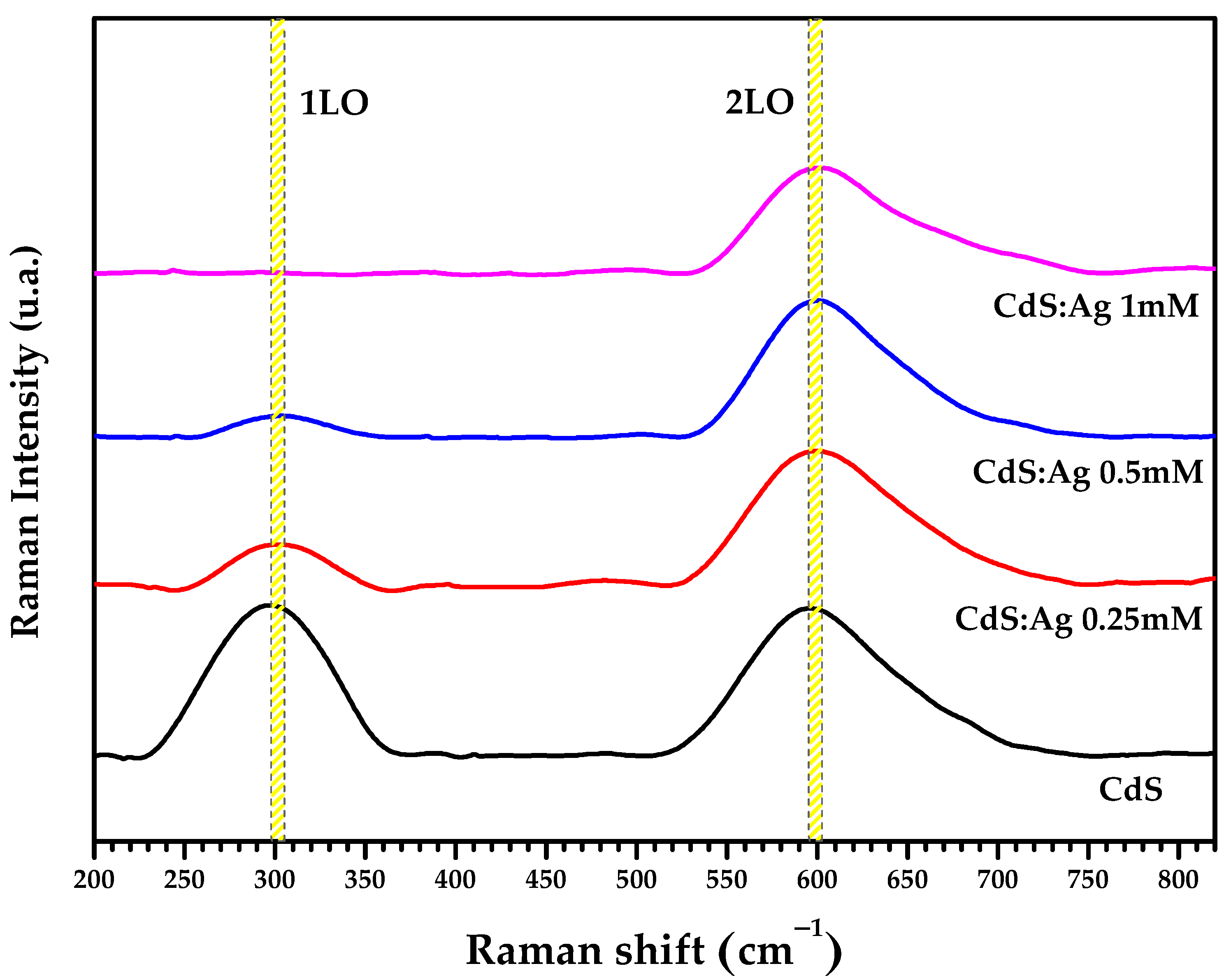
3.3. Raman Spectroscopy Analysis

Raman spectroscopy is an optical technique based on the inelastic scattering of light as it interacts with the sample. The change in frequency of the emitted photons is a signature and explains the different frequency modes, such as vibrational, rotational and other low-frequency transitions in molecules. This contributes to the identification of lattice structural defects, orientation and crystalline quality of the materials [35,36]. Thus, this technique can be useful for the analysis of vibrational and structural characteristics of thin films. However, in the case of CdS thin films, it cannot be used to clearly identify the crystalline structure, because the frequencies of the cubic modes practically coincide with that of the hexagonal modes [17,37].
Figure 5 shows the Raman spectra of the Ag-doped CdS and CdS thin films in the range from 200 to 800 cm−1. Two distinct Raman peaks are visible in the spectra for all the thin films except for the CdS:Ag 1 mM film, which shows only one characteristic peak. The first Raman peak in the region around 300 cm−1 is identified as the first longitudinal optical phonon vibration (1LO), while the Raman peak around 600 cm−1 is the second longitudinal optical phonon (2LO). The locations of the 1LO and 2LO Raman peaks for all samples are reported in Table 2. These peaks of polycrystalline CdS thin films are consistent with that reported for the hexagonal structure of CdS, whose first and second frequencies of the 1LO and 2LO modes are generally found around 305 cm−1 and 604 cm−1 [35,38,39,40]. Close values have also been reported for the cubic structure of CdS in more recent studies [17,41], hence the limitation of being able to index the crystal structure from these peaks.
According to Table 2, the peaks obtained for CdS and CdS:Ag thin films associated with 1LO and 2LO modes are comparable with the data reported by Taur et al. [21] who obtained values of 303 cm−1 and 600 cm−1 for the Raman shift in Ag-doped CdS thin films. In this study, it can be observed that the 1LO and 2LO Raman bands of the synthesized thin films shift towards lower frequencies with increasing Ag concentration up to 0.5 mM. This shift is caused by the effect of grain size and particle size reduction [42]. When the grain size drops to a few nanometers, phonon confinement occurs, resulting in line asymmetry around the Raman band maximum and a shift towards low frequencies compared to the CdS thin film. Crystallinity, stress defects and non-spherical geometry of the nanostructures play an important role in the shift of the 1LO and 2LO modes towards lower frequencies [40,41,43].
No additional Raman bands were observed due to Ag impurities. However, according to the spectra in Figure 5, the intensity of the peak associated with the 1LO mode decays with increasing Ag concentration, until disappearing almost by complement for the highest concentration (1 mM). This effect is due to the stress induced by the interstitial incorporation of Ag in the crystal lattice of CdS [34], indicating that high concentrations are not favorable for doping, which is consistent with what was revealed in XDR. In addition to the frequency shift in the 1LO and 2LO modes, the FWHM is another important parameter that provides information about the crystallinity, induced strain and purity of the material. The increase in FWHM or broadening of the 1LO and 2LO peaks of CdS:Ag thin films (see Table 2) indicates a decrease in crystal size and surface roughness [41].
For polycrystalline CdS and CdS:Ag thin films, the spin–phonon (sp) ratio corresponding to the intensity ratio of the 2LO mode to the 1LO mode was calculated. It is a way to evaluate the electron–phonon exchange interaction. As seen in Table 2, the intensity ratio I2/I1 in the Ag-doped samples (0.25 mM and 1 mM) is higher than that in the pure CdS thin film. This indicates a strong coupling (sp) and is due to the understanding of the unit cell volume [44]. The crystal quality Q is the reciprocal of the spin–phonon (sp) interaction. Therefore, the I2/I1 ratios are also used to determine the crystal quality [45,46]. For a perfect crystal, the Q factor is equal to zero. Furthermore, it is known that the crystal quality of a sample depends on the number of oxygen atoms present on the crystal surface [34]. Therefore, the best crystal quality among the films synthesized in this research and with the strongest existence of spin–phonon (sp) interactions was obtained for the CdS:Ag 0.25 mM thin film. For this sample, there is a higher amount of oxygen atoms on the crystal surface, which occupy a minimum surface area that increases the mobility of the atoms on the surface and, therefore, improves the quality of this crystal.

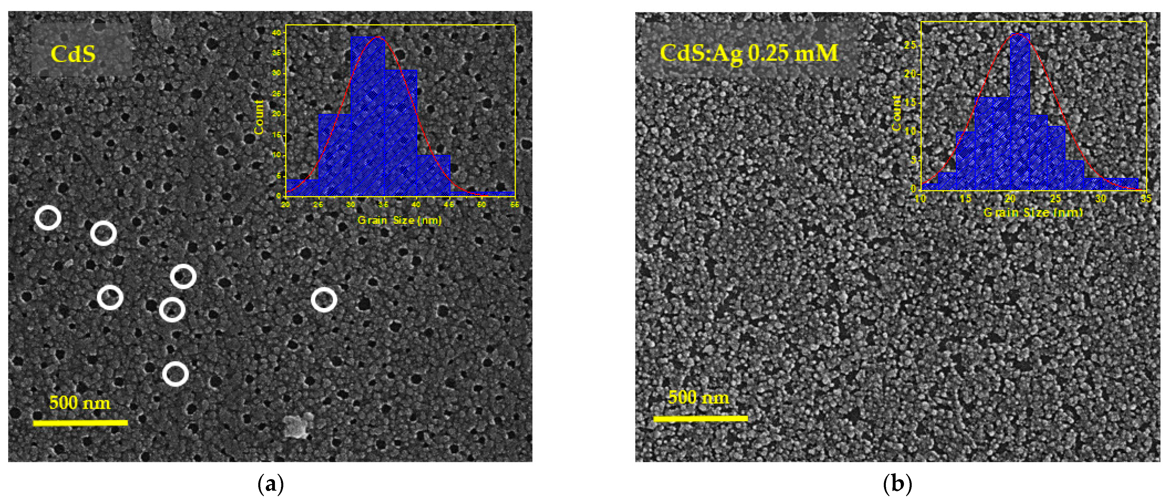
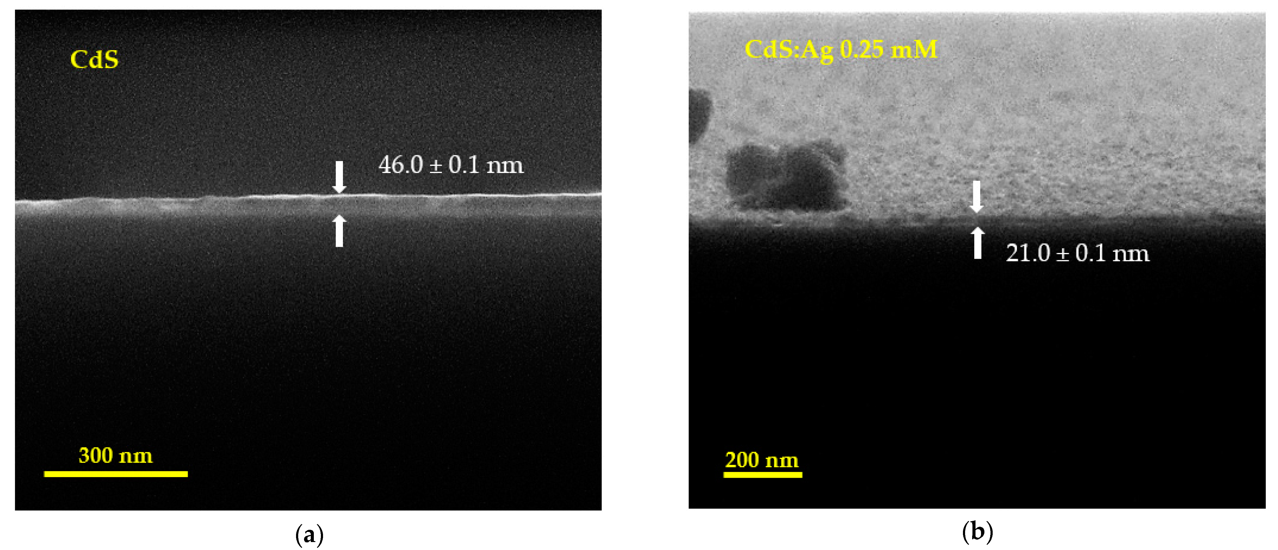
3.4. Surface Morphology Analysis

The morphological structure of chalcogenide films has a significant influence on their properties. This aspect is particularly important for solar cells, since both grain boundary and surface roughness directly affect the recombination process in such films. As a consequence, the surface morphology and the presence of impurities will influence the conversion efficiency of the photovoltaic device [47].
The set of images in Figure 6, exposes the front section of CdS thin films (a) and CdS doped at 0.25 mM (b), 0.5 mM (c), and 0.1 mM (d). These images were obtained using the Helios 5 PFIB CXe electron microscope at 10.00 kV with a magnification of 100,000×.
According to the images in Figure 6, the CdS thin film is composed of granular nanostructures, densely agglomerated and uniformly distributed on the substrate, with relatively spherical morphologies and average sizes of 34 nm. The dark areas enclosed in a white circle correspond to regions of the substrate that were not coated during the synthesis. This result is in agreement with that obtained by M. Husham, et al. [48], who synthesized CdS thin films using the microwave-assisted chemical bath technique (MACBD) and observed the formation of granules with sizes of 30, 32 and 36 nm when using CdCl2 as a source of cadmium ions at molar concentrations of 0.10 M, 0.06 M and 0.08 M, respectively. The formation of granules with quasi-spherical morphologies can be attributed to the spheroid structure of the sulfur ions [36]. Other techniques have succeeded in obtaining CdS thin films with similar morphologies, as is the case of the magnetron sputtering technique, which allowed obtaining CdS films with thicknesses of 100 nm, constituted by nanograins uniformly adhered to the substrate and with average sizes of 30–50 nm in a pure Ar environment [49].
On the other hand, in the Ag-doped CdS films, granular nanostructures with undefined morphologies are observed, with a decrease in grain size with respect to the pristine CdS thin film. The average grain sizes for the 0.25 mM and 0.5 mM doped samples were 21 nm, while for the 1 mM doped sample, it was 38 nm. In Figure 6b,c, the films doped with Ag are at 0.25 mM and 0.5 mM correspondingly, and it is observed that the particle density grows uniformly and adheres homogeneously to the substrate; however, the CdS:Ag sample at 1 mM (Figure 6d) presents a polydispersion of the size and a remarkable separation between the boundary of the granules. For solar cell applications, this aspect is especially important, since grain boundaries and surface homogeneity have a direct effect on the recombination of the film with the constituent layers of the heterostructure and, thus, on the energy conversion efficiency [27,36,50]. In this sense, CdS:Ag thin films at 0.25 mM and 0.5 mM could exhibit the best morphological properties for this application.
As for the thickness of the layers, Figure 7a shows the SEM micrograph of the cross-section of the CdS thin film. This image was obtained at a scale of 300 nm, with a beam of 20.00 kV and a magnification of 200,000×. The thin film was found to be approximately 46.0 ± 0.1 nm thick. On the other hand, for the sample doped with Ag at 0.25 mM (Figure 7b), the thickness was 21.0 ± 0.1 nm and this value was not significantly modified for the other doping concentrations.
Given the equivalent deposition conditions in which all the samples were synthesized, the images presented in Figure 6 and Figure 7 confirm that the CdS and CdS:Ag films, especially the pure CdS and CdS:Ag 0.25 mM sample, are ultra-thin, homogeneous and uniform.
The energy dispersive spectroscopy (EDS) technique provided the semi-quantitative analysis of the chemical composition of the CdS and CdS:Ag thin film samples. Figure 8 presents the EDS spectra of the doped CdS and CdS thin films. These spectra confirm the presence of the expected elements cadmium (Cd) and sulfur (S) in all the prepared samples, in addition to the elements silicon (Si), oxygen (O) sodium (Na), aluminum (Al), magnesium (Mg), calcium (Ca), attributed to the soda-lime glass substrate [51,52]. The compositional atomic ratios of Cd and S in the thin films are described in Figure 9. It is observed that for the pure CdS thin film, the atomic ratio of cadmium and sulfur is 21.14% and 78.86%, respectively. This is consistent with the presence of elemental sulfur in the diffractograms. The excess sulfur in the CdS thin film can be attributed to the chemical environment of the synthesis, particularly the high content of CS(NH)2 in the precursor solution. The molar concentrations of cadmium (CdCl2, 0.05 M) and sulfur (CS(NH)2, 0.5 M) precursors in the synthesis have a molar ratio of 1:10 (Cd:S), which may confirm the reason for the significant excess of sulfur compared to cadmium.
For the doped samples, the Cd/S ratio decreases due to the effect of the doping concentration. The Ag element could not be detected through this technique due to the low doping concentrations. However, according to Figure 9, it was found that the Cd/S ratio decreases significantly with increasing Ag molar concentration. The lowest Cd/S ratio of 0.20 was for the CdS thin film prepared using 1 mM (0.001 M) Ag concentration. This confirms that, for high doping, Ag atoms enter more at the interstitial sites than at the substitution sites [27], which is consistent with that revealed by Raman spectra and XDR analysis. No elements other than those present in the glass were detected, confirming the purity of the grown thin films.

3.5. Optical Analysis

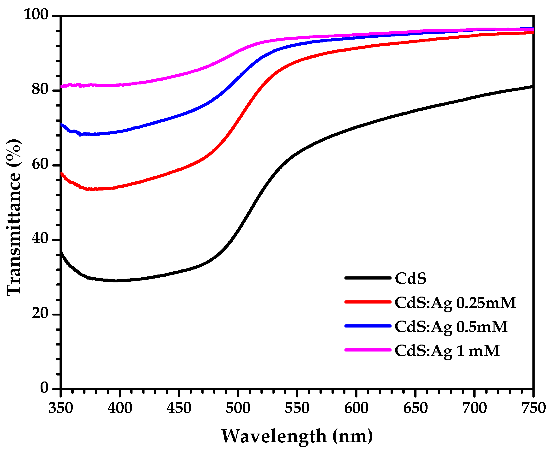
3.5.1. Spectral Transmittance

Optical transmittance spectra of CdS and CdS:Ag thin films were obtained to study the effect of silver doping concentration on the optical characteristics of CdS thin films. In Figure 10, the optical transmittance spectra for wavelengths ranging from 350 to 750 nm are shown. The black curve corresponds to the pristine CdS thin film and the red, blue and magenta curves correspond to the silver-doped CdS thin films at concentrations of 0.25 mM, 0.5 mM and 1 mM, respectively.
The transmittance of all the films is above 60%, which is desirable for use as a window layer in solar cells; meanwhile, it can be observed that, in the Ag-doped films, the average transmittance in the visible region increased. This is due to the fact that when Ag+2 ions are incorporated into the CdS lattice, the crystallization growth of CdS was moderated to form a thinner and less rough surface, as could be observed in the SEM images. As a consequence, there would be a reduction in the optical dispersion of the material and, with this, an improvement in the spectral transmittance response [53,54].

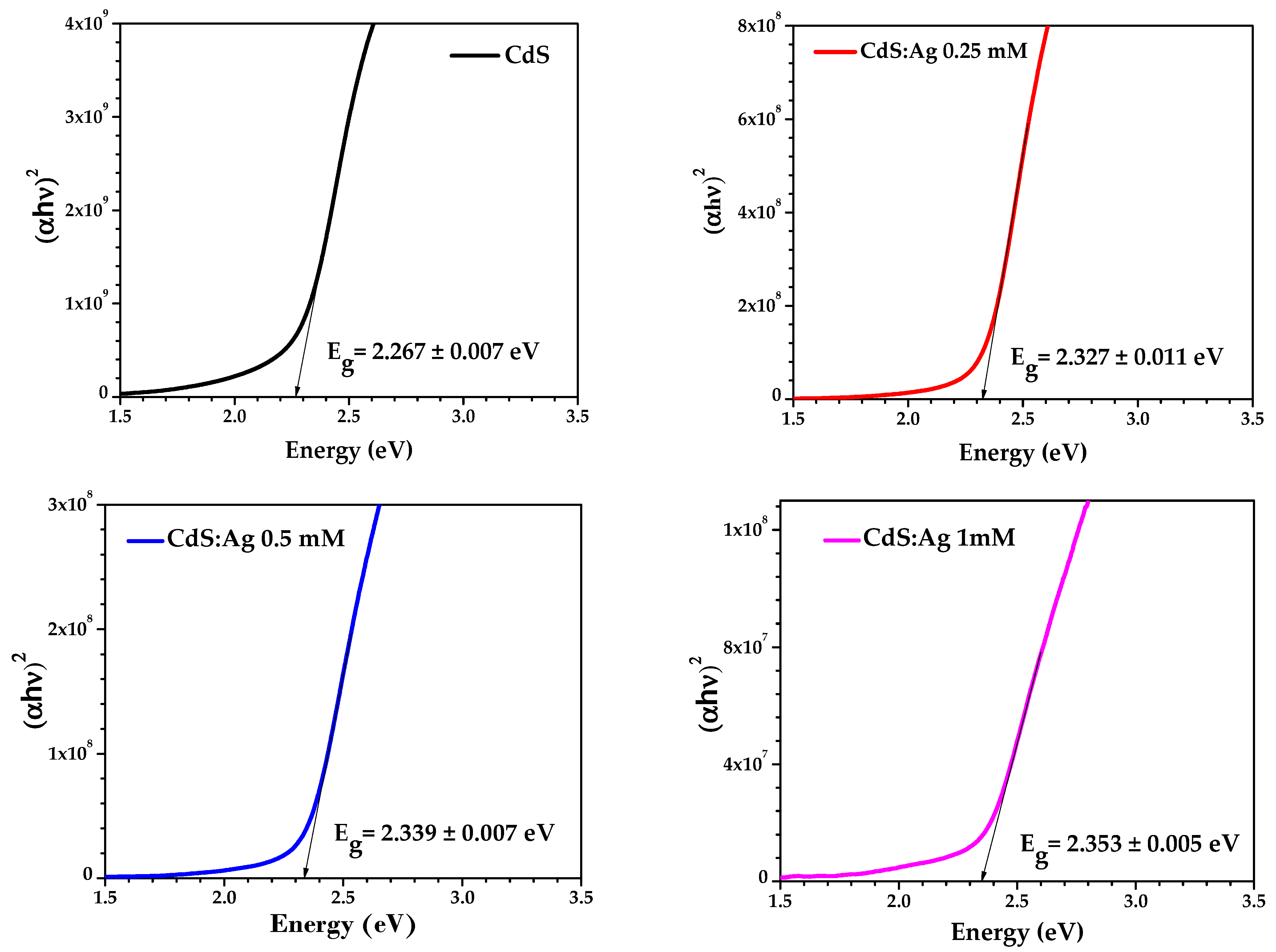
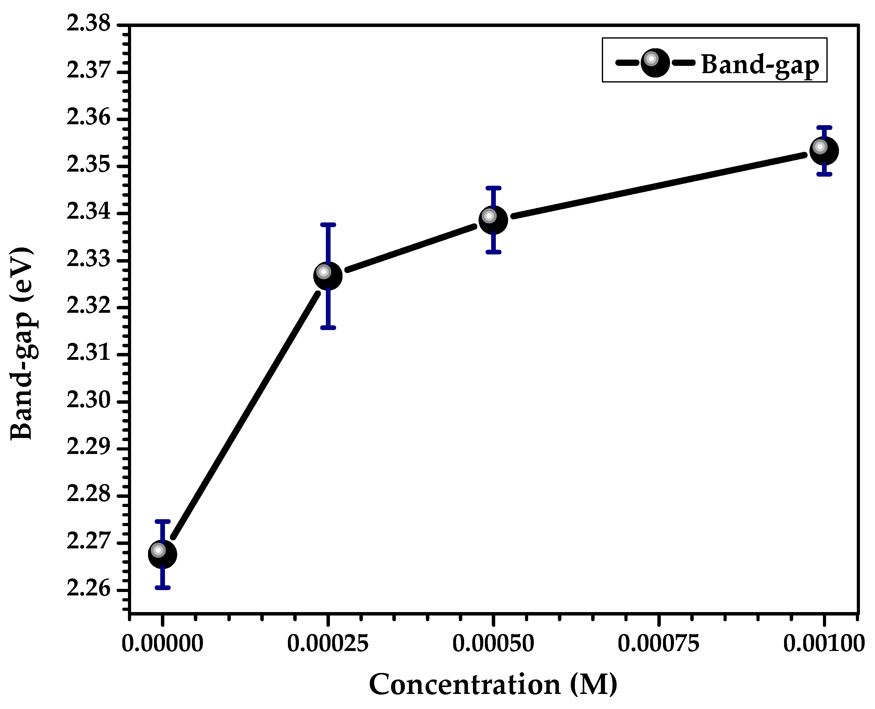
3.5.2. Optical Band Gap

CdS thin films are low-dimensional systems characterized by direct electronic transitions in the visible range. The optical band gap of the deposited films was determined according to the Tauc model.
Figure 11 shows the linear approximations made to the absorption limit for the CdS and CdS:Ag samples. These approximations gave the optical forbidden bands and show that the lowest forbidden band was 2.267 ± 0.007 eV for the pristine CdS sample, and the highest was 2.353 ± 0.005 eV for the CdS:Ag sample doped to 1 mM. The Eg value of the CdS thin film of 2.267 ± 0.007 eV, which is relatively low compared to bulk CdS (2.42 eV), and may be associated with the short deposition time and position of the substrate in the reactor. This is in agreement with the work published by Ashok et al., and Ruiz-Ortega et al., who obtained values of 2.30 eV and 2.24 eV, respectively [7,36]; on the other hand, the increase in Eg of the CdS:Ag thin films with respect to the pure CdS thin film can be assigned to the defects generated by the dopant ions.
Figure 12 shows the dependence of the forbidden band on Ag concentration in CdS thin films. There is a tendency for the energy of the band gap to increase with increasing doping concentration, up to 2.353 ± 0.005 eV for the CdS:Ag 1 mM (0.001 M) sample. This behavior is attributed to the Moss–Burstein effect, because the dopant ions create interstitial defects that perturb the lattice of the crystal structure, enough to shift the Fermi level towards the conduction band, causing the band gap of the material to increase [44]. The defects generated at the edge of the conduction band are responsible for the enhancement in the band gap, as this allows the absorption edge to shift to shorter wavelengths, leading to higher energies. As a result, all energy levels near the conduction band edge are filled and the gap value is increased.

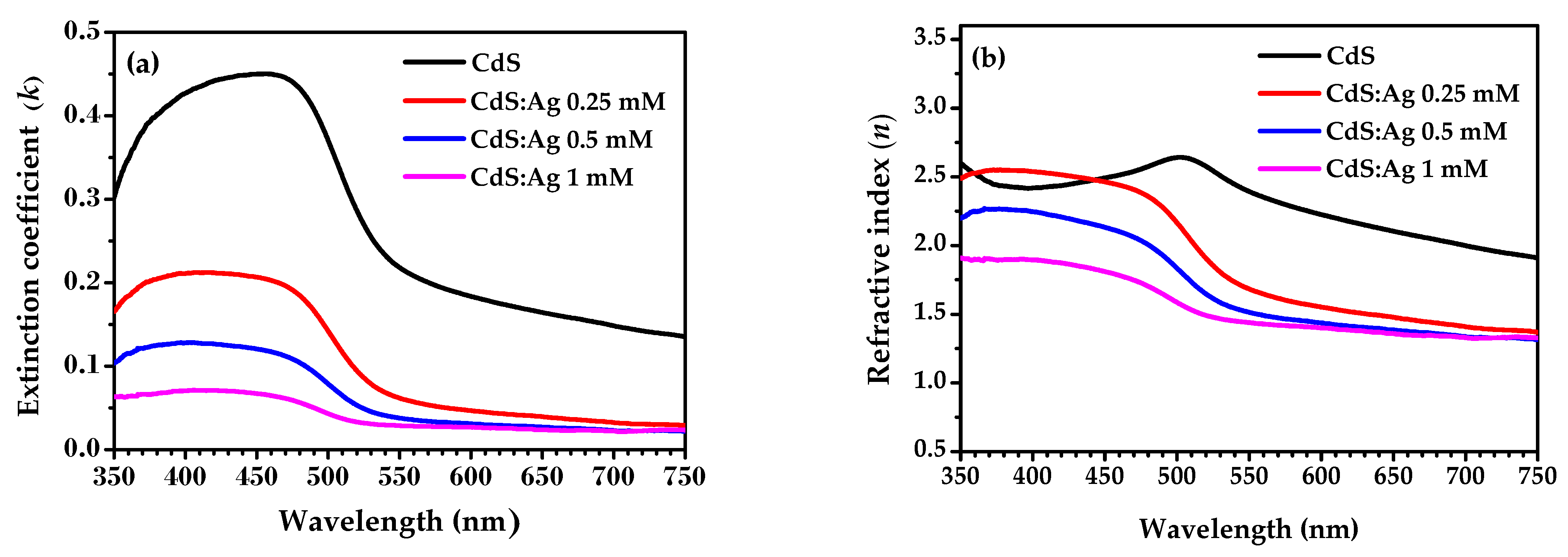
3.5.3. Extinction Coefficient and Refractive Index

The evaluation of the extinction coefficient and refractive index of thin films plays an important role in the designation of fundamental optical parameters for optoelectronic devices where these structures are implemented.
The variation of extinction coefficient (k) and refractive index (n) of CdS and CdS:Ag thin films for the wavelength range from 350 to 750 nm are shown in Figure 13a,b, respectively. These are explained by Equations (3) and (5), as described in Section 2.1.
The optical coefficients (n) and (k) of thin films have a significant correlation with the structural and morphological properties in terms of grain sizes primarily. According to Figure 13a, the k values of CdS and doped CdS thin films vary from 0.45 to 0.02 in the visible range with the effect of doping concentration. The optical absorption is consistent with these curves and indicates that the doped films absorb weakly in the 550–750 nm range. These k values are in agreement with other previously published work on doped CdS thin films [32,34,55]. On the other hand, according to Figure 13b, the CdS thin films show a similar trend for the refractive index, decreasing from 2.6 to 1.31 after the incorporation of doping. This behavior can be attributed to an increase in the porosity of the thin films or a decrease in grain size that allows the electromagnetic propagation response to be much faster, which adds significant value for the implementation of these layers in optoelectronic devices such as solar cells and photodetectors [34,41].

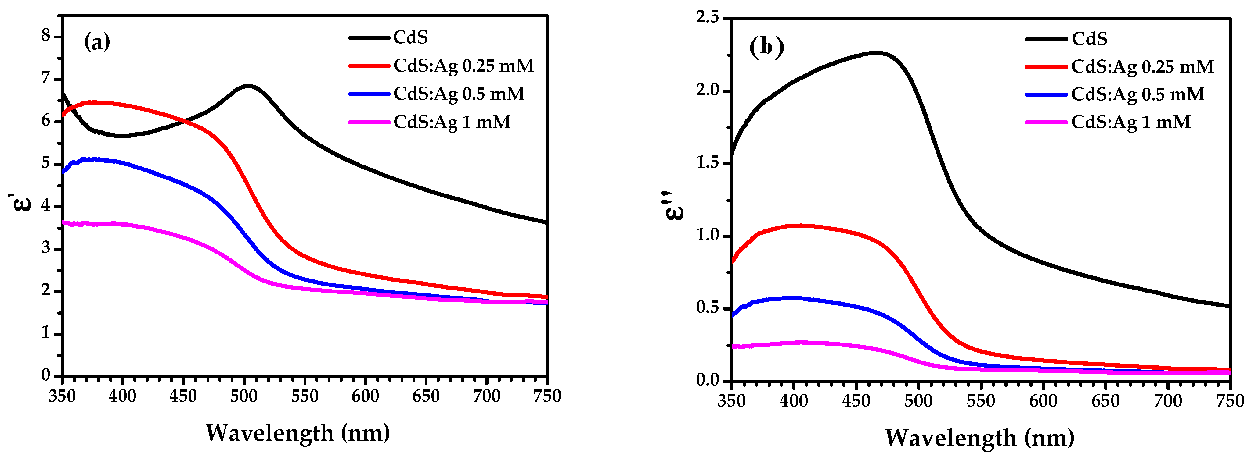
3.5.4. Dielectric Constant

Figure 14 shows the variation of the dielectric constant ( ε ) and dielectric loss ( ε ) spectra as a function of wavelength in the visible spectrum, for CdS and CdS:Ag thin films. The complex dielectric function ε * of the materials is represented by ε * = ε + i ε . Figure 14a shows the values of the dielectric constant in the range from 1.6 to 7. It is observed that the dielectric constant of the CdS thin film decreases with increasing Ag concentration in most of the visible spectrum. Above 550 nm, the dielectric constant is observed to reach a nearly constant value. The decrease in ε at longer wavelengths (low frequencies) can be attributed to the large electrostatic binding force, which arises due to space charge polarization near the grain boundary interfaces [56].
When an electric field is incident on the crystal surface, charges are spatially rearranged, electric dipoles are produced, and changes in dipole moments result in rotational polarization; however, the large electrostatic binding force makes this polarization state mostly weak over much of the visible spectrum. Figure 14b shows the variation of dielectric loss in the range of 0.2 to 2.3. These curves show that the dielectric loss depends on the frequency of the applied field, comparable to that of the dielectric constant. The dielectric loss decreases with increasing wavelength for all samples, comparable to that of the dielectric constant, but appears to reach saturation in the lower frequency range for all doped films.
Table 3 summarizes the different parameters determined from the structural, morphological and optical characterizations for each of the CdS and CdS:Ag samples synthesized in this research.

4. Conclusions

Se CdS:Ag thin films were successfully deposited by bath chemical synthesis and with different doping molar concentrations. The structural analysis confirmed the crystallization of CdS in the hexagonal phase in the (1 0 1), (1 0 2) and (0 0 4) planes for all samples, diffractograms reveal doping favorability at low concentrations, revealing the formation of Ag2S for the CdS:Ag 0.25 mM CdS:Ag thin film.
Morphological characterization of the CdS thin film revealed that the coating was diffused by spherical granular nanostructures with an average size of 34 nm which were uniformly distributed on the substrate. The Ag-doped films presented nanostructures with undefined morphologies, with average sizes of 21 nm for 0.25 mM and 0.5 mM concentrations, and 38 nm for 1 mM. Cross-sections revealed thicknesses of 46.0 ± 0.1 for the pristine CdS sample and 21.0 ± 0.1 nm for the Ag-doped samples. The set of SEM micrographs confirms that the CdS and CdS:Ag 0.25 mM thin films are ultra-thin, homogeneous and uniform.
The optical response of all films reported that the spectral transmittance of the CdS thin film was around 60% in the visible range. After incorporation of the Ag dopant, the absorption edge was shifted towards shorter wavelengths with increasing concentration, leading to a higher spectral transmittance response in most of the visible spectrum. The band gap of the pristine CdS thin film was 2.267 ± 0.007 eV, while that of the doped samples was 2.327 ± 0.011, 2.339 ± 0.007 and 2.353 ± 0.005 eV for the concentrations of 0.25 mM, 0.5 mM and 1 mM, respectively.
The overall results of this study categorize CdS and CdS:Ag 0.25 mM thin films as potential candidates for use as n-type optical window layers in heterojunction solar cells.
This study opens up several possibilities for the use of CdS:Ag thin films not only in photovoltaic applications, but also in the field of optoelectronics and photonic devices. The modification of the band gap and the quality of the coatings even after the incorporation of Ag doping suggests their potential in optical sensors, photodetectors and light-emitting devices. Future studies can explore the optimization of doping concentration and improvement of optical properties by using different dopants or deposition methods. In addition, the interaction between the formed nanostructures and the evaluation of their impact on energy conversion efficiency deserves further analysis, with a view to their practical implementation in large-scale applications.

Author Contributions

Conceptualization, J.P.M.-J. and S.D.H.-P.; methodology, S.D.H.-P. and S.J.C.; validation, D.A.A., J.L.I. and S.J.C.; formal analysis, S.D.H.-P., D.A.A. and S.J.C.; investigation, J.P.M.-J.; resources, J.L.I. and D.A.A.; data curation, J.P.M.-J.; writing—original draft preparation, J.P.M.-J. and S.D.H.-P.; writing—review and editing, J.P.M.-J., S.D.H.-P., D.A.A. and S.J.C.; visualization, D.A.A. and S.J.C.; supervision, D.A.A. and S.J.C.; funding acquisition, D.A.A. and J.L.I. All authors have read and agreed to the published version of the manuscript.

Funding

This research was financed by Science, Technology and Innovation of the Sistema General de Regalías (SGR)—Colombia through the project “Formación de Capital Humano maestría y Doctorado para el departamento del CesarUniversidad Popular del Cesar–Nacional with BPIN code 2021000100130, and the project “Formación de Capital Humano de Alto NivelUniversidad Popular del Cesar–Nacional with BPIN code 2019000100010.

Institutional Review Board Statement

Not applicable.

Informed Consent Statement

Not applicable.

Data Availability Statement

Data are contained within the article.

Acknowledgments

The authors would like to acknowledge the Universidad Popular del Cesar for providing the facilities of the optics and informatics laboratory for the partial development of this research.

Conflicts of Interest

The authors declare no conflicts of interest.

References

  1. Buonomenna, M.G. Inorganic thin-film solar cells: Challenges at the terawatt-scale. Symmetry 2023, 15, 1718. [Google Scholar] [CrossRef]
  2. Tamilselvan, S.N.; Shanmugan, S. Towards sustainable solar cells: Unveiling the latest developments in bio-nano materials for enhanced DSSC efficiency. Clean Energy 2024, 8, 238–257. [Google Scholar] [CrossRef]
  3. Perera, A.T.; Nik, V.M.; Chen, D.; Scartezzini, J.L.; Hong, T. Quantifying the impacts of climate change and extreme climate events on energy systems. Nat. Energy 2020, 5, 150–159. [Google Scholar] [CrossRef]
  4. Di Carlo, V.; Prete, P.; Dubrovskii, V.G.; Berdnikov, Y.; Lovergine, N. CdTe Nanowires by Au-catalyzed metalorganic vapor phase epitaxy. Nano Lett. 2017, 17, 4075–4082. [Google Scholar] [CrossRef] [PubMed]
  5. Hussein, R.D.; Jafir, A.O. A review on physical properties of CdS thin film. J. Phys. Chem. Funct. Mater. 2022, 5, 40–50. [Google Scholar] [CrossRef]
  6. Ismail, W.; Ibrahim, G.; Habib, M.A.; Alduaij, O.K.; Abdelfatah, M.; El-Shaer, A. Advancement of physical and photoelectrochemical properties of nanostructured CdS thin films toward optoelectronic applications. Nanomaterials 2023, 13, 1764. [Google Scholar] [CrossRef]
  7. Ruiz, R.C.; Esquivel, L.A.; Gonzalez, M.A.; Hernandez, C.; Matsumoto, Y.; Albor, M.D.L. Comprehensive Analysis of CdS Ultrathin Films Modified by the Substrate Position inside the Reactor Container Using the CBD Technique. ACS Omega 2023, 8, 31725–31737. [Google Scholar] [CrossRef] [PubMed]
  8. Mathur, A.S.; Singh, B.P. Study of effect of defects on CdS/CdTe heterojunction solar cell. Optik 2020, 212, 164717. [Google Scholar] [CrossRef]
  9. Lovergine, N.; Cingolani, R.; Mancini, A.M.; Ferrara, M. Photoluminescence of CVD grown CdS epilayers on CdTe substrates. J. Cryst. Growth 1992, 118, 304–308. [Google Scholar] [CrossRef]
  10. Irvine, S.J.; Stafford, A.; Ahmed, M.U.; Prete, P.; Berrigan, R. MOVPE of II–VI materials. Prog. Cryst. Growth Charact. Mater. 1997, 35, 177–206. [Google Scholar] [CrossRef]
  11. Fathima, M.I.; Arulanantham, A.M.S.; Wilson, K.J. Effect of ZnS nanowire ARC on CZTS/CdS thin film solar cell by Nebulizer Spray Pyrolysis Technique. Mater. Res. Express. 2020, 7, 015510. [Google Scholar] [CrossRef]
  12. Nadarajah, M.; Gour, K.S.; Singh, V.N. Sputtered cadmium sulfide (CdS) buffer layer for kesterite and chalcogenide thin film solar cell (TFSC) Applications. J. Nanosci. Nanotechnol. 2020, 20, 3909–3912. [Google Scholar] [CrossRef]
  13. Chen, Z.; Ashokan, A.; Russo, S.P.; Mulvaney, P. Temperature Dependence of the CdS Bandgap in the Extreme Confinement Regime. Nano Lett. 2023, 23, 9287–9294. [Google Scholar] [CrossRef] [PubMed]
  14. Yücel, E.; Şahin, O. Effect of pH on the structural, optical and nanomechanical properties of CdS thin films grown by chemical bath deposition. Ceram. Int. 2016, 42, 6399–6407. [Google Scholar] [CrossRef]
  15. El-Shaer, A.; Ezzat, S.; Habib, M.A.; Alduaij, O.K.; Meaz, T.M.; El-Attar, S.A. Influence of Deposition Time on Structural, Morphological, and Optical Properties of CdS Thin Films Grown by Low-Cost Chemical Bath Deposition. Crystals 2023, 13, 788. [Google Scholar] [CrossRef]
  16. Najm, A.S.; Al-Azawi, N.M.; Ibrahim, S.A.; Al-Adili, A.; Ahmed, N.M.; Al-Jumaili, B.E. Mechanism of chemical bath deposition of CdS thin films: Influence of sulphur precursor concentration on microstructural and optoelectronic characterizations. Coatings 2022, 12, 1400. [Google Scholar] [CrossRef]
  17. Contreras, J.I.; Diaz, J.; Flores, A.; Morales, R.L.; Álvarez, M.E.; Balderas, J.A. Structural and optical modifications of CdS properties in CdS-Au thin films prepared by CBD. Results Phys. 2021, 22, 103914. [Google Scholar] [CrossRef]
  18. Herrera, D.; Diosa, J.E.; Fernández, A.; Mosquera, E. Influence of aluminum doping on structural, morphological, vibrational, and optical properties of CdS thin films obtained by chemical bath deposition. Mater. Sci. Eng. B 2021, 273, 115451. [Google Scholar] [CrossRef]
  19. Molina, J.; Horta, S.D.; Espejo, L.F.; Castillo, S.J.; Ávila, D.A. Comparative study of the optical response in thin films of CdS:In. J. Phys. Conf. Ser. 2021, 1723, 012028. [Google Scholar] [CrossRef]
  20. Diaz, O.I.; Berman, D.; Flores, A.; López, R.; Ramos, A.; Álvarez, M.E. Cu-doped CdS thin films by chemical bath deposition and ion exchange. J. Mater. Sci. Mater. Electron. 2020, 31, 1722–1730. [Google Scholar] [CrossRef]
  21. Taur, V.S.; Joshi, R.A.; Sharma, R. Annealing-induced modifications in physicochemical and optoelectronic properties of Ag-doped nanostructured CdS thin films. Int. J. Photoenergy 2012, 2012, 264027. [Google Scholar] [CrossRef]
  22. Ferrá, S.R.; Berman, D.; García, R.; Castillo, S.J.; Ramírez, R.; Gnade, B.E.; Quevedo, M.A. Optical and structural properties of CdS thin films grown by chemical bath deposition doped with Ag by ion exchange. Optik 2014, 125, 1533–1536. [Google Scholar] [CrossRef]
  23. Flores, A.; Contreras, J.I.; Diaz, J.; Angel, P.D.; Enríquez, J.P.; Castillo, S.J.; Álvarez, M.E. Stimulation of the photoluminescent properties of CBD-CdS thin films achieved by structural modifications resulting from Ag⁺ doping. Phys. Status Solidi RRL 2017, 11, 1700134. [Google Scholar] [CrossRef]
  24. Najm, A.S.; Aljuhani, A.; Naeem, H.S.; Sopian, K.; Ismail, R.A.; Holi, A.M.; Moria, H. Mechanism and principle of doping: Realizing of silver incorporation in CdS thin film via doping concentration effect. RSC Adv. 2022, 12, 29613–29626. [Google Scholar] [CrossRef] [PubMed]
  25. Rahman, M.M.; Karim, M.R.; Alharbi, H.F.; Aldokhayel, B.; Uzzaman, T.; Zahir, H. Cadmium selenide quantum dots for solar cell applications: A review. Chem. Asian J. 2021, 16, 902–921. [Google Scholar] [CrossRef]
  26. Shuklov, I.A.; Razumov, V.F. Lead chalcogenide quantum dots for photoelectric devices. Russ. Chem. Rev. 2019, 89, 379. [Google Scholar] [CrossRef]
  27. Patterson, A.L. The Scherrer formula for X-ray particle size determination. Phys. Rev. 1939, 56, 978. [Google Scholar] [CrossRef]
  28. Tauc, J.; Grigorovici, R.; Vancu, A. Optical properties and electronic structure of amorphous germanium. Phys. Status Solidi 1966, 15, 627–637. [Google Scholar] [CrossRef]
  29. Cingolani, R.; Di Dio, M.; Lomascolo, M.; Rinaldi, R.; Prete, P.; Vasanelli, L.; Vanzetti, L.; Bassani, F.; Bonanni, A.; Sorba, L.; et al. Photocurrent Spectroscopy of Zn1-xCdxSe/ZnSe Quantum Wells in p-i-n Heterostructures. Phys. Rev. B 1994, 50, 12179–12182. [Google Scholar] [CrossRef]
  30. Rahman, M.F.; Hossain, J.; Ismail, A.B.M. Structural, surface morphological and optical properties and their correlation with the thickness of spin coated superior quality CdS thin film synthesized using a novel chemical route. SN Appl. Sci. 2020, 2, 1956. [Google Scholar] [CrossRef]
  31. Pankove, J.I. Optical Processes in Semiconductors, 2nd ed.; Dover Publications, Inc.: Mineola, NY, USA, 1975; pp. 87–94. [Google Scholar]
  32. Shkir, M.; Khan, Z.R.; Chandekar, K.V.; Alshahrani, T.; Ashraf, I.M.; Khan, A.; Sanaa, M.F. Facile fabrication of Ag/Y: CdS/Ag thin films-based photodetectors with enhanced photodetection performance. Sens. Actuators A Phys. 2021, 331, 112890. [Google Scholar] [CrossRef]
  33. Islam, M.A.; Hossain, M.S.; Aliyu, M.M.; Chelvanathan, P.; Huda, Q.; Karim, M.R.; Amin, N. Comparison of structural and optical properties of CdS thin films grown by CSVT, CBD and sputtering techniques. Energy Procedia 2013, 33, 203–213. [Google Scholar] [CrossRef]
  34. Trabelsi, A.B.G.; Chandekar, K.V.; Alkallas, F.H.; Ashraf, I.M.; Hakami, J.; Shkir, M.; AlFaify, S. A comprehensive study on Co-doped CdS nanostructured films fit for optoelectronic applications. J. Mater. Res. Technol. 2022, 21, 3982–4001. [Google Scholar] [CrossRef]
  35. Rondiya, S.; Rokade, A.; Gabhale, B.; Pandharkar, S.; Chaudhari, M.; Date, A.; Jadkar, S. Effect of bath temperature on optical and morphology properties of CdS thin films grown by chemical bath deposition. Energy Procedia 2017, 110, 202–209. [Google Scholar] [CrossRef]
  36. Ashok, A.; Regmi, G.; Romero, A.; Solis, M.; Velumani, S.; Castaneda, H. Comparative studies of CdS thin films by chemical bath deposition techniques as a buffer layer for solar cell applications. J. Mater. Sci. Mater. Electron. 2020, 31, 7499–7518. [Google Scholar] [CrossRef]
  37. Zahn, D.R.T.; Maierhofer, C.; Winter, A.; Reckzügel, M.; Srama, R.; Rossow, U.; Richter, W. In situ monitoring of heterostructure growth by optical spectroscopies: CdS on InP (110). Appl. Surf. Sci. 1992, 56, 684–690. [Google Scholar] [CrossRef]
  38. Nusimovici, M.A.; Balkanski, M.; Birman, J.L. Lattice dynamics of wurtzite: CdS. II. Phys. Rev. B 1970, 1, 595. [Google Scholar] [CrossRef]
  39. Marshall, R.; Mitra, S.S. Optically active phonon processes in CdS and ZnS. Phys. Rev. 1964, 134, A1019. [Google Scholar] [CrossRef]
  40. Trajić, J.; Gilić, M.; Romčević, N.; Romčević, M.; Stanišić, G.; Hadžić, B.; Yahia, Y.S. Raman spectroscopy of optical properties in CdS thin films. Sci. Sinter. 2015, 47, 145–152. [Google Scholar] [CrossRef]
  41. Sharma, B.; Lalwani, R.; Das, R. Spectroscopic studies of CdS nanocrystalline thin films synthesized by sol–gel spin coating technique for optoelectronic application: Influence of co-doping. Braz. J. Phys. 2023, 53, 42. [Google Scholar] [CrossRef]
  42. Peng, Y.; Hu, X.; Xu, X.; Chen, X.; Peng, J.; Han, J.; Dimitrijev, S. Temperature and doping dependence of the Raman scattering in 4H-SiC. Opt. Mater. Express 2016, 6, 2725–2733. [Google Scholar] [CrossRef]
  43. Sharma, R.; Sharma, K.S.; Kumar, D. Introduction to Nanotechnology. In Nanomaterials in Clinical Therapeutics: Synthesis and Applications; Sharma, R., Ed.; Springer: Cham, Switzerland, 2022; pp. 1–31. [Google Scholar] [CrossRef]
  44. Olvera, R.; De Moure, F.; Mayén, S.A.; Quiñones, J.; Centeno, A.; Sosa, A.; Santos-Cruz, J. Effect of indium doping on structural, optical and electrical properties of cadmium sulfide thin films. Chalcogenide Lett. 2020, 17, 329–336. [Google Scholar] [CrossRef]
  45. Budde, M.; Tschammer, C.; Franz, P.; Feldl, J.; Ramsteiner, M.; Goldhahn, R.; Bierwagen, O. Structural, optical, and electrical properties of unintentionally doped NiO layers grown on MgO by plasma-assisted molecular beam epitaxy. J. Appl. Phys. 2018, 123, 195301. [Google Scholar] [CrossRef]
  46. Panigrahi, U.K.; Das, P.K.; Biswal, R.; Sathe, V.; Babu, P.D.; Mitra, A.; Mallick, P. Zn doping induced enhancement of multifunctional properties in NiO nanoparticles. J. Alloys Compd. 2020, 833, 155050. [Google Scholar] [CrossRef]
  47. Zheng, L.; Zhang, D.; Ma, Y.; Lu, Z.; Chen, Z.; Wang, S.; Gong, Q. Morphology control of the perovskite films for efficient solar cells. Dalton Trans. 2015, 44, 10582–10593. [Google Scholar] [CrossRef]
  48. Husham, M.; Hassan, Z.; Mahdi, M.A.; Selman, A.M.; Ahmed, N.M. Fabrication and characterization of nanocrystalline CdS thin film-based optical sensor grown via microwave-assisted chemical bath deposition. Superlattices Microstruct. 2014, 67, 8–16. [Google Scholar] [CrossRef]
  49. Islam, M.A.; Misran, H.; Akhtaruzzaman, M.; Amin, N. Influence of oxygen on structural and optoelectronic properties of CdS thin film deposited by magnetron sputtering technique. Chin. J. Phys. 2020, 67, 170–179. [Google Scholar] [CrossRef]
  50. Sahraei, R.; Shahriyar, S.; Majles Ara, M.H.; Daneshfar, A.; Shokri, N. Preparation of nanocrystalline CdS thin films by a new chemical bath deposition route for application in solar cells as antireflection coatings. Prog. Color Color. Coat. 2011, 3, 82–90. [Google Scholar] [CrossRef]
  51. Baltakesmez, A.; Aykaç, C.; Güzeldir, B. Phase transition and changing properties of nanostructured V₂O₅ thin films deposited by spray pyrolysis technique, as a function of tungsten dopant. Appl. Phys. A 2019, 125, 1–18. [Google Scholar] [CrossRef]
  52. Bintari, P.L.; Purwanto, H.; Marzuki, A. Characterization of soda-lime glass with aluminum doping as a planar wave guide using electric-field-assisted solid-state ion exchange method. J. Phys. Conf. Ser. 2019, 1153, 012084. [Google Scholar] [CrossRef]
  53. Lee, J.H.; Park, B.O. Transparent conducting ZnO: Al, In and Sn thin films deposited by the sol–gel method. Thin Solid Film. 2003, 426, 94–99. [Google Scholar] [CrossRef]
  54. Tsay, C.Y.; Cheng, H.C.; Tung, Y.T.; Tuan, W.H.; Lin, C.K. Effect of Sn-doped on microstructural and optical properties of ZnO thin films deposited by sol–gel method. Thin Solid Film. 2008, 517, 1032–1036. [Google Scholar] [CrossRef]
  55. Petrus, R.Y.; Ilchuk, H.A.; Kashuba, A.I.; Semkiv, I.V.; Zmiiovska, E.O.; Honchar, F.M. Optical properties of CdS thin films. J. Appl. Spectrosc. 2020, 87, 35–40. [Google Scholar] [CrossRef]
  56. Suresh, S.; Arunseshan, C. Dielectric properties of cadmium selenide (CdSe) nanoparticles synthesized by sol-vothermal method. Appl. Nanosci. 2014, 4, 179–184. [Google Scholar] [CrossRef]
Figure 1. Schematic diagram of the synthesis of CdS and CdS:Ag thin films.
Coatings 15 00431 g001
Figure 2. Photograph of thin films of (a) CdS, (b) CdS:Ag 0.25 mM, (c) CdS:Ag 0.5 mM and (d) CdS:Ag 1 mM.
Coatings 15 00431 g002
Figure 3. XDR patterns of CdS and Ag-doped CdS thin films.
Coatings 15 00431 g003
Figure 4. Relation of crystallite size to doping concentration in CdS and CdS:Ag thin films.
Coatings 15 00431 g004
Figure 5. Raman spectra of CdS and CdS:Ag thin films.
Coatings 15 00431 g005
Figure 6. SEM micrographs of the front section of CdS (a), CdS:Ag thin films at 0.25 mM (b), 0.5 mM (c) and 1 mM (d).
Coatings 15 00431 g006aCoatings 15 00431 g006b
Figure 7. SEM micrographs of the cross-section of CdS (a), CdS:Ag (b) thin films.
Coatings 15 00431 g007
Figure 8. EDS spectra of CdS and CdS:Ag thin films.
Coatings 15 00431 g008
Figure 9. EDS compositional details and Cd/S ratios in CdS and CdS:Ag thin films.
Coatings 15 00431 g009
Figure 10. UV-Vis transmittance spectra of CdS thin films (black curve), CdS:Ag at 0.25 mM (red curve), 0.5 mM (blue curve) and 1 mM (magenta curve).
Coatings 15 00431 g010
Figure 11. Linear approximations for obtaining the band gap of CdS and CdS:Ag thin films.
Coatings 15 00431 g011
Figure 12. Optical band gap behavior of CdS:Ag thin films as a function of doping concentration.
Coatings 15 00431 g012
Figure 13. Spectra of (a) extinction coefficient (k) and (b) refractive index (n) of CdS and CdS:Ag thin films.
Coatings 15 00431 g013
Figure 14. (a) Dielectric constant (ε′) and (b) dielectric loss (ε″) of CdS and CdS:Ag thin films.
Coatings 15 00431 g014
Table 1. Precursor materials for the synthesis of CdS and CdS:Ag thin films, and their respective molar concentrations.
Precursors
Line: Merck Group, Sigma-Aldrich,
Burlington, MA, USA.
Molar Concentration
Cadmium chloride/CdCl2 ≥ 99.99%0.05 M
Sodium citrate/C6H7Na3O7•2H2O ≥ 99.0%0.5 M
Potassium hydroxide/KOH ≥ 85% pellets0.3 M
Buffer Solution pH 10.00-
Thiourea/CS(NH2) ≥ 99.0%0.5 M
Silver nitrate/AgNO3 ≥ 99.85%0.25 mM, 0.5 mM y 1 mM
Table 2. Raman spectroscopy analysis of CdS and CdS:Ag thin films.
Samples1LO Mode2LO Mode
Raman Shift
±0.01 (cm−1)
FWHM
±0.01 (cm−1)
Raman Shift
±0.01 (cm−1)
FWHM
±0.01 (cm−1)
s p = I 2 ( L O ) I 1 ( L O ) Q = 1 s p
CdS296.6577.24595.3395.470.981.02
CdS:Ag 0.25 mM302.4385.75599.06115.461.420.70
CdS:Ag 0.5 mM303.40113.78600.40107.091.320.75
CdS:Ag 1 mM601.75143.96
Table 3. Calculated structural, morphological and optical parameters of CdS and CdS:Ag ultra-thin films.
SampleDep. Time ± 0.1 (min)Dep. Temperature ± 0.1 (°C)Crystallite Size (D) (nm)Quality Factor (Q)Thickness ± 0.1 (nm)Eg (eV)
CdS15.060.022.33 ± 0.421.0246.02.267 ± 0.007
CdS:Ag 0.25 mM15.060.0 10.29 ± 0.280.7021.02.327 ± 0.011
CdS:Ag 0.5 mM15.060.0 10.86 ± 0.090.7521.02.339 ± 0.007
CdS:Ag 1 mM15.060.0 17.28 ± 0.23-21.02.353 ± 0.005
Disclaimer/Publisher’s Note: The statements, opinions and data contained in all publications are solely those of the individual author(s) and contributor(s) and not of MDPI and/or the editor(s). MDPI and/or the editor(s) disclaim responsibility for any injury to people or property resulting from any ideas, methods, instructions or products referred to in the content.

