Article

A Study of the Hall Effect on Doped and Undoped Praseodymium Nickelate Perovskite Thin Films and the Impact of the Reduction Process

CRISMAT, CNRS, Normandie Université, Département PCI, ENSICAEN, UNICAEN, 6, boulevard du Maréchal Juin, F-14050 Caen, France
*
Authors to whom correspondence should be addressed.
Coatings 2025, 15(3), 287; https://doi.org/10.3390/coatings15030287
Submission received: 10 January 2025 / Revised: 19 February 2025 / Accepted: 27 February 2025 / Published: 1 March 2025

Abstract

:
PrNiO3 and Pr0.8Sr0.2NiO3 epitaxial thin films were deposited by pulsed laser deposition (PLD) on different substrates and studied for Hall effect and resistivity behavior. Conductive behavior is observed in the doped composition, and a normal Hall effect allows to determine charge carrier’s density and mobility. The doped compositions show a high concentration of charge carriers (≈1023 cm−3 at 300 K), and it appears that they can be controlled by the strains. Sr doping enhances the transport properties, leading to a transition from semiconducting to metallic behavior. The impact of the reduction process on charge carrier concentration and mobility is also studied.

1. Introduction

In 2019, superconductivity properties have been highlighted in an infinite-layer phase of nickelate thin films, with a critical temperature of 14.9 K [1]. Initially, the composition of those phases was Nd0.8Sr0.2NiO2/SrTiO3, but quickly research was reoriented towards other lanthanide elements like lanthanum and praseodymium. Other compositions showed the same superconductivity properties, depending on the doping level of strontium and evidence a superconducting dome [2].
To obtain such an infinite layer, a synthesis of the perovskite phase is necessary. A topotactic reduction using CaH2 evolves the perovskite phase into the infinite layer phase; however, this process is hard to control. A study of the Hall effect in undoped perovskite shows a conventional effect. In a doped infinite layer, depending on the strontium doping level [3], the carrier’s type can change following the temperature (holes at high temperature, electrons at low temperature). The aim of our work is to compare the doped and undoped composition on the transport properties and the impact of the strain by the substrate. The strontium doping induces a different charge distribution, as the introduction of Sr2+ modifies the valence balance compared to the system with only Nd3+. The substitution of Sr2+ for Nd3+ leads to a mixed charge state, influencing the electronic distribution and potentially altering the charge ordering pattern within the structure.
High-quality perovskites lanthanides nickelates are the first requirement to obtain the superconducting infinite layer. The mechanism of superconductivity in the infinite layer of Pr0.8Sr0.2NiO2 and Nd0.8Sr0.2NiO2 may be explained by NiO2 planes [1]. A high-quality infinite layer with a low thickness (7–15 nm [4]) is needed to reach superconductivity. The low thickness is a key factor needed to obtain homogenous phases. Nevertheless, the topotactic reduction with CaH2 is a complicated process that may induce defects in the structure. A study of the impact of the reduction process on the transport properties of the doped composition deposited on SrTiO3 substrate is also conducted.
This work characterizes the doped composition before the reduction to understand the impact of the doping and of the reduction processes on the transport properties.

2. Experimental Section

Thins films were prepared via the pulsed laser deposition (PLD) technique using an ultraviolet KrF excimer laser with a wavelength of 248 nm.
Targets of PrNiO3 and Pr0.8Sr0.2NiO3 were prepared by standard solid-state reaction route.
The thin films were grown on SrTiO3 (001) (STO) and (LaAlO3)0.3(Sr2TaAlO6)0.7 (001) (LSAT). They were grown at 600 °C in an oxygen atmosphere (10−1 mbar after a previous vacuum at 10−8 mbar) with a laser energy of 180 and 200 mJ, corresponding to a fluence of around 1.6–2.0 J.cm−2. The laser rate was fixed at 2 Hz. The thin films were grown with a thickness of around 20 nm. A topotactic reduction was performed following the process described in the work of Hoshang et al. [5]. The samples were placed in sealed tube with 0.5 g of CaH2 and heated at 260 °C at a rate of 5 °C/min. The samples were reduced for 3 h and cooled to the room temperature at a rate of 5 °C/min. Crystal structure of perovskite thin films was characterized using Cuα radiation (0.15406 nm), with X-ray diffraction (XRD) in θ:2θ configuration on D8 Discover (BRUKER).
The Hall effect and resistivity measurements were performed on a Physical Properties Measurements System (PPMS). The Hall effect measurements were performed in a Van der Paw configuration, at different temperatures, under a magnetic field (varying from −9 T to 9 T). Resistivity measurements were performed using four-probe geometry.

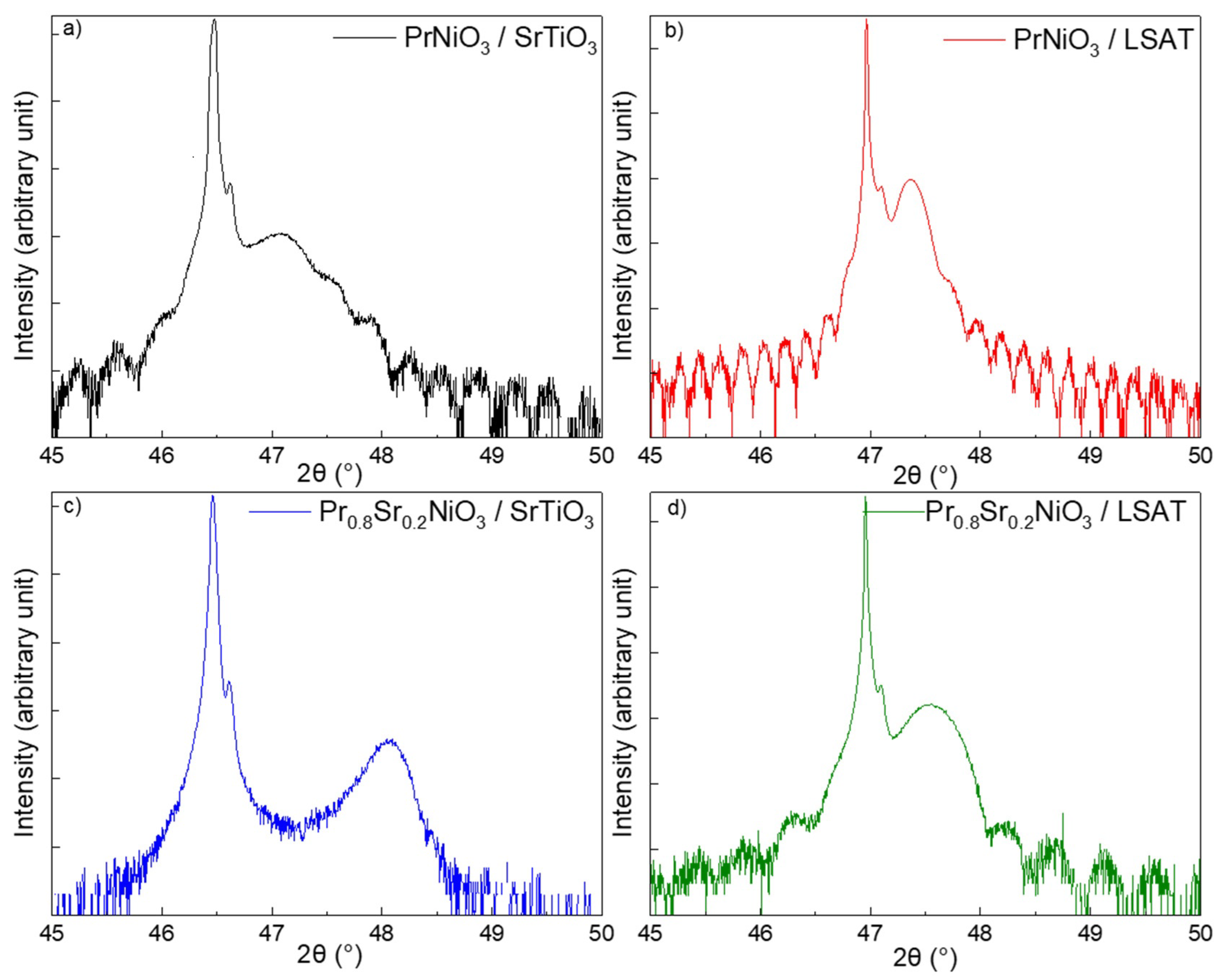
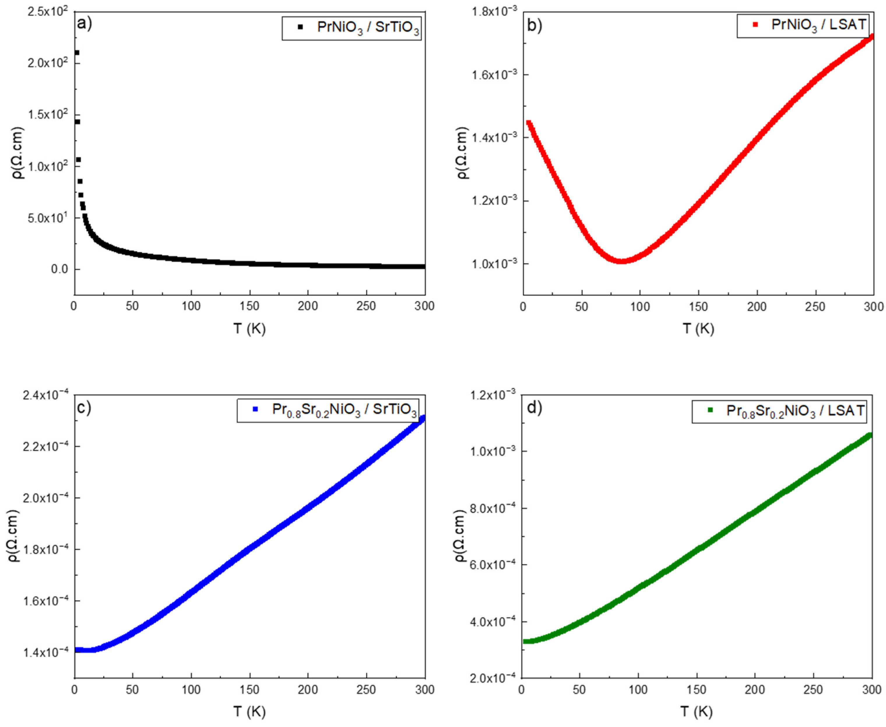
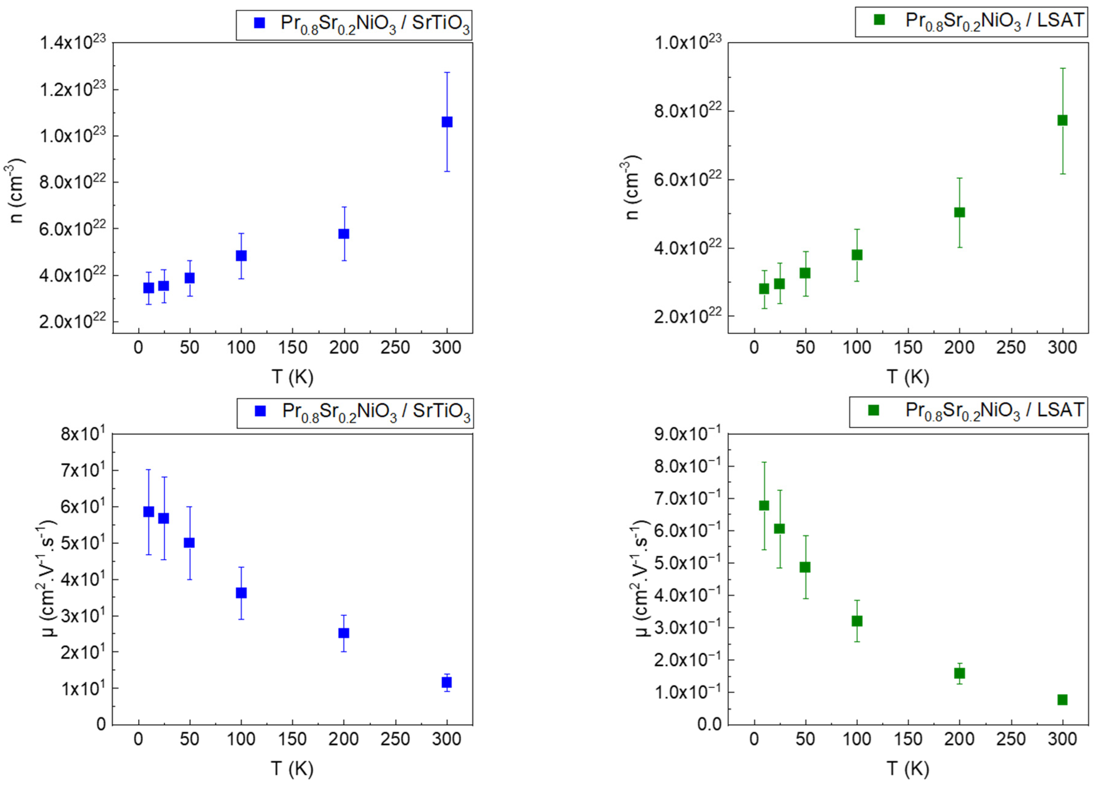
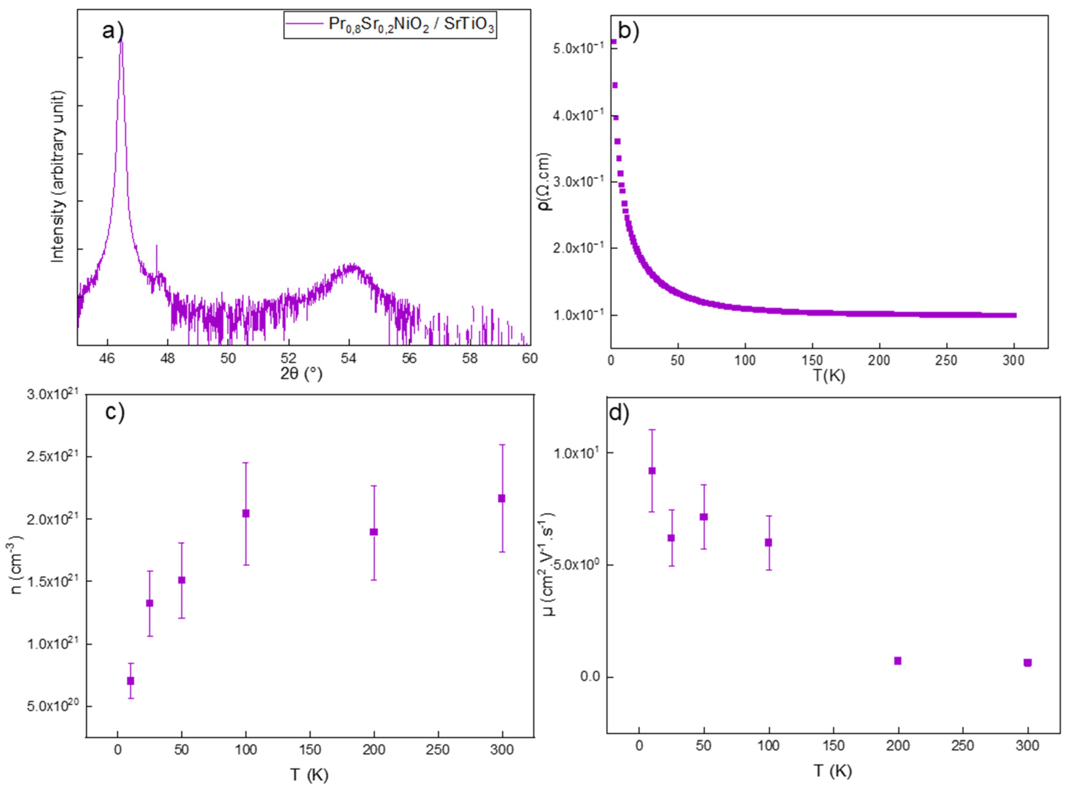
3. Results and Discussion

In this work, a study of the effect of the composition (PrNiO3 and Pr0.8Sr0.2NiO3) and of the strain (SrTiO3 and LSAT substrate) is performed. We focused on the positive strain.
The strain is calculated by the following formula:
σ % = a s u b s t r a t e a b u l k a s u b s t r a t e
Figure 1 illustrates the XRD pattern of thin films and the substrate (002). The intense and thin peaks correspond to the substrate peak (SrTiO3 2θ = 46.47° and LSAT 2θ = 46.97°, which represent the commercial value). The lowest intensity peaks and oscillations correspond to thin films. Fringes and an absence of other orientations indicate a high quality of crystallization. The out-of-plane parameter is also shown (Table 1). The thin films deposited on the LSAT substrate were grown with a better crystalline quality due to a lower induced strain (Table 1). The limited strain allows the thin films to obtain better crystallinity.
Thin films are constrained in-plane, leaving the out-of-plane lattice parameter as the only degree of freedom. As the in-plane strain increases, this degree of freedom leads to greater deformation, resulting in more structural defects.
Table 2 shows that the out-of-plane parameters calculated correspond to the characteristics of the perovskite phase (3.84 Å for undoped perovskite and 3.80 Å for doped perovskite) [6,7,8,9]. As already reported for PrNiO3/SrTiO3 composition, oxygen vacancies can lead to an increase in the out-of-plane parameters [6].
A diffraction peak is measured at 48° for the Pr0.8Sr0.2NiO3 deposited on SrTiO3 (Figure 1c). The small position shift in the pick to lower angle (47.7°) on Pr0.8Sr0.2NiO3 deposited on LSAT (Figure 1d) can be a sign of a Ruddlesden Popper phase (RP) [10]. The study of the quality of the thin film via XRD before the reduction is therefore essential to have an initial idea about the presence of the perovskite phase. This work characterizes the doped composition before and after the reduction. To synthesize the infinite layer, it is necessary to achieve a topotactic reduction in a pure perovskite with a high quality.
Undoped ReNiO3 nickelates have been studied for a few years for the metallic insulator transition (MIT) [11]. The temperature of this transition depends on the lanthanide. The heavier the atom is, the higher the MIT is. In the case of Pr in bulk and thin fims, the temperature of the MIT is 90 K [7,11]. As already reported for PrNiO3 thin films, the strain can tune the transport properties of the thin films [12].
A semi-conductor behavior for PrNiO3/SrTiO3 is presented in Figure 2a. This composition can adopt different behaviors depending on the oxygen vacancies inside the thin films, insulating or presenting a metallic insulator transition at 110 K [9]. The insulating behavior is characteristic of an undoped composition with oxygen vacancies, as already reported by the XRD [6]. Figure 2b illustrates a metal insulator transition at 90 K in the LSAT substrate, the value is already reported and is characteristic of a high-quality PrNiO3 thin film [9].
As shown in Figure 2c,d, both behaviors exhibit the metallic characteristics of doped Pr0.8Sr0.2NiO3 compositions. This observation is consistent with the previous results found in the literature [7]. Depending on the fluence of the deposition, a small upturn can be observed at a low temperature [10], like in our doped composition on SrTiO3. The thin film deposited on LSAT is metallic in all the temperature range measurement.
To understand the mechanisms of conduction in the samples, more transport measurements are necessary. The Hall effect measurements in Van der Paw configuration were performed. From these measurements, the carrier’s concentration can be extracted. The mobility of the carrier’s charges is deduced by the carrier’s concentration and the resistivity of our samples. The carrier’s concentration and charges mobility are measured for all the samples.
The charge carrier density NH is calculated with the following formula: NH = 1/etRH, where RH is the slope, e is the charge and t is the thickness of the thin film. The mobility µH is calculated by the formula µH = 1/eρNH (with being e the charge, ρ the resistivity and NH the carrier concentration).
As shown in Figure 3, the carrier’s density of PrNiO3/LSAT is established at 3.5 × 1022 cm−3 holes h+ for all the temperature measurements range (10–300 K) (Figure 3). The carrier’s density is two times superior to the deposition on SrTiO3 due to the strain induced by the substrate.
The mobility is stable for both compositions, but the deposition on the LSAT presents a higher mobility than the thin film deposited on SrTiO3 (respectively, 0.15 cm2.V−1.s−1 and 0.0004 cm2.V−1.s−1). The high difference is caused by the difference in resistivity (much larger for PrNiO3/SrTiO3). The charge carrier’s concentration is rather constant with the temperature.
In the literature, SmNiO3 was reported to be a semi-conducting material with a Hall effect dependent on the temperature. This effect is called the Hopping Hall effect. In that study, for the undoped composition, we did not observe the same effect, indicating that not all lanthanide nickelates exhibit the same behavior.
As reported in [13], the carriers’ density in LaNiO3 is 3 × 1022 cm−3 and 1022 cm−3 for ReNiO3.
ReNiO3 has a high concentration of charge carriers, and the resistivity is low due to the d7 electronic configuration of Ni3+ [14]. This electronic configuration has already been reported in SmNiO3: t2g6 eg1 [15]. The presence of an unpaired electron allows the structure to be highly conductive with charge carriers of high mobility.
As shown in Figure 4, the doped composition Pr0.8Sr0.2NiO3 on both substrates presents a conventional Hall effect. The doped composition Pr0.8Sr0.2NiO3 deposited on SrTiO3 and LSAT presents the same charge carrier’s density from 3 × 1022 cm−3 at 10 K to 9 × 1023 cm−3 at 300 K. That charge carrier’s concentration is in the same order as in the undoped composition.
The doped composition deposited on SrTiO3 presents a high mobility, between 10 and 60 cm2.V−1.s−1, which is four decades more than the deposition on LSAT.
As previously reported [16], the appearance of another phase in nickelate thin films is usual. That secondary phase is the Ruddlesden Popper impurity An+1BnO3n+1. The most common RP is (Pr0.8Sr0.2)2NiO4 which presents an insulating behavior. This low mobility can be explained by the presence of a very small fraction of Ruddlesden Popper impurity in the thin films. The presence of the two phases is an obstacle for the mobility of charge carriers.
Despite the temperature dependence of the Hall effect, this system does not exhibit a Hopping Hall effect. This confirms the inhomogeneous nature of the system.
Despite the high thickness of the doped perovskites, we performed the topotactic reduction on the Pr0.8Sr0.2NiO3 deposited on SrTiO3 to study the impact of the reduction on the transport properties.
In Figure 5a, the XRD pattern shows the presence of an infinite layer phase with an out of plane parameter 3.34 Å, which is characteristic of this phase [3]. Nevertheless, this phase presents inhomogeneity, likely due to the high thickness and the difficulty in reducing the entire thin film in an infinite layer. This inhomogeneity is observable with the perovskite peak, which remains present at 47.7°. This suggests that the transport properties are probably impacted by the coexistence of the two phases. Transport measurements were performed to more precisely characterize the thin film.
In Figure 5b, resistivity measurements show semi-conducting behavior. We tried to fit the experimental resistivity data with the different modes (Arrhenius, Variable rampe hopping, Efros-Shklovskii) of a homogenous disordered system but we were not successful. Most likely it is consistent with the inhomogeneity noted in Figure 5a.
To understand the mechanism of transport in the infinite layer, Hall effect measurements were carried out to determine the charge carrier concentration and the mobility. In Figure 5c, the charge carrier concentration is stable, at 2 × 1021 cm−3 at a high temperature (25–300 K), and decreases to 7 × 1020 cm−3 at a low temperature (10 K). The reduction process led to a decrease in the charge carrier concentration.
The mobility measured is low at a high temperature (0.7 cm2.V−1.s−1) but increases significantly at a temperature lower than 100 K (between 6 and 9.7 cm2.V−1.s−1 (Figure 5d)) Those values are diminished after the reduction by factor six.
The reduction process has a high impact on the transport properties. Indeed, the mechanism of the transport changes from metallic to semiconductor. The charge carrier’s concentration and mobility decreases a lot.
Reduction causes a transition from the perovskite phase to an infinite phase. However, the presence of impurities limits the charge transport by further reducing the already low mobility of the charge carriers due to the structure. Structural defects induced by the phase transition cause local disorder, disrupting the overall crystal order and leading to a decrease in charge carrier mobility and transport efficiency. This decrease is also induced by the inhomogeneity of the system, as evidenced by X-ray measurements.
To optimize the reduction process, a high-quality perovskite with a low thickness appears to be a key factor in achieving superconductivity. However, the deposition of a capping layer protects the thin film from excessive reduction. Another safer way to reduce the thin films is to use a metallic capping layer to capture oxygen from the perovskite and reduce it in an infinite layer [17].
In the existing literature [3] on superconducting infinite layer phases with neodymium of 20 nm, the charge carrier concentration is estimated at 2.5 × 1023 cm−3 with a mobility of 0.025 cm2.V−1.s−1. In thick infinite layers, the transport behavior is completely different, and presents a lower concentration of charge carriers, but a higher mobility. This difference in transport properties could explain why we cannot observe superconductivity in thick thin films, when the infinite phase signal does exist.

4. Conclusions

Thin films of doped and undoped praseodymium nickelate perovskite were synthesized by pulsed laser deposition. High quality perovskites were prepared as X-Ray Diffraction and transport measurements evidence. Doped perovskite presented a high charge carrier concentration (≈1023 cm−3 at 300 K), but their mobility was very different. This parameter could be explained by the presence of a secondary phase Ruddlesden Popper in the thin film deposited on the LSAT. The Pr0.8Sr0.2NiO3 deposited on the SrTiO3 presents the high-quality perovskite phase necessary to obtain the infinite layer. The Pr0.8Sr0.2NiO3 has a higher value of the carrier density and mobility than the infinite layer due to a better metallic behavior. The infinite layer Pr0.8Sr0.2NiO2 presents a semi-conducting behavior and charge carrier’s concentration and mobility are highly impacted by the reduction process. The emergence of superconductivity in infinite-layer nickelates is strongly correlated with their thickness.

Author Contributions

Conceptualization: A.D. and A.P.; supervision A.D.; formal analysis: A.M., M.K., Y.B. and W.P.; investigation: A.M., A.D. and A.P.; funding acquisition: A.D. and A.P.; writing—original draft: A.M.; writing—review and editing: A.M., A.D. and A.P. All authors have read and agreed to the published version of the manuscript.

Funding

This work is supported by ANR SUPERNICKEL (ANR-21-CE30-0041). This work is supported by Région Normandie Caen Université.

Institutional Review Board Statement

Not applicable.

Informed Consent Statement

Not applicable.

Data Availability Statement

Data are contained within the article.

Acknowledgments

I would like to acknowledge Fabien Veillon. I would also like to acknowledge Daniele Preziosi and Hoshang Sahib.

Conflicts of Interest

The authors declare no conflicts of interest.

References

  1. Li, D.; Lee, K.; Wang, B.Y.; Osada, M.; Crossley, S.; Lee, H.R.; Cui, Y.; Hikita, Y.; Hwang, H.Y. Superconductivity in infinite layer nickelates. Nature 2019, 572, 624–627. [Google Scholar] [CrossRef] [PubMed]
  2. Chow, L.E.; Ariando, A. Infinite-Layer Nickelate Superconductors: A Current Experimental Perspective of the Crystal and Electronic Structures. Front. Phys. 2022, 10, 834658. [Google Scholar] [CrossRef]
  3. Osada, M.; Wang, B.Y.; Lee, K.; Li, D.; Hwang, H.Y. Phase diagram of infinite layer praseodymium nickelate Pr1−xSrxNiO2 thin films. Phys. Rev. Mater. 2020, 4, 121801. [Google Scholar] [CrossRef]
  4. Lee, K.; Goodge, B.H.; Li, D.; Osada, M.; Wang, B.Y.; Cui, Y.; Kourkoutis, L.F.; Hwang, H.Y. Aspects of the Synthesis of Thin Film Superconducting Infinite-Layer Nickelates. APL Mater. 2020, 8, 041107. [Google Scholar] [CrossRef]
  5. Sahib, H.; Rosa, F.; Raji, A.; Merzoni, G.; Ghiringhelli, G.; Salluzzo, M.; Gloter, A.; Viart, N.; Preziosi, D. Superconductivity in PrNiO2 Infinite-Layer Nickelates. arXiv 2024, arXiv:2410.16147. [Google Scholar]
  6. Harisankar, S.; Chandra, M.; Das, S.; Soni, K.; Prajapat, M.; Mavani, K.R. Anomalous Hall effect and re-entrant metallic transitions in epitaxial PrNiO3−δ thin films. J. Appl. Phys. 2018, 125, 025102. [Google Scholar]
  7. Gutiérrez-Llorente, A.; Raji, A.; Zhang, D.; Divay, L.; Gloter, A.; Gallego, F.; Galindo, C.; Bibes, M.; Iglesias, L. Toward Reliable Synthesis of Superconducting Infinite Layer Nickelate Thin Films by Topochemical Reduction. Adv. Sci. 2024, 11, e2309092. [Google Scholar] [CrossRef] [PubMed]
  8. Venimadhav, A.; Lekshmi, I.C.; Hegde, M. Strain-induced metallic behavior in PrNiO3 epitaxial thin films. Mater. Res. Bull. 2002, 37, 201–208. [Google Scholar] [CrossRef]
  9. Harisankar, S.; Soni, K.; Yadav, E.; Mavani, K.R. Strain-mediated effects of oxygen deficiency and variation in non-Fermi liquid behavior of epitaxial PrNiO3−δ thin films. J. Phys. Condens. Matter 2019, 31, 135601. [Google Scholar] [CrossRef] [PubMed]
  10. Keenari, M. Study of Reduction Process on Perovskite Nickelates and Its Derivatives: A Bulk and Thin Film Approach. Ph.D. Thesis, Normandie Université, Caen, France, 2023. [Google Scholar]
  11. Torrance, J.B.; Lacorre, P.; Nazzal, A.I.; Ansaldo, E.J.; Niedermayer, C. Systematic study of insulator-metal transitions in perovskites RNiO3 (R = Pr, Nd, Sm, Eu) due to closing of charge-transfer gap. Phys. Rev. B 1992, 45, 8209–8212. [Google Scholar] [CrossRef] [PubMed]
  12. Kumar, A.; Singh, P.; Kaur, D.; Jesudasan, J.; Raychaudhuri, P. Substrate effect on electrical transport properties of RNiO3 thin films prepared by pulsed laser deposition. J. Phys. D Appl. Phys. 2006, 39, 5310. [Google Scholar] [CrossRef]
  13. Noun, W.; Berini, B.; Dumont, Y.; Dahoo, P.R.; Keller, N. Correlation between electrical and ellipsometric properties on high-quality epitaxial thin films of the conductive oxide LaNiO3 on STO (001). J. Appl. Phys. 2007, 102, 063709. [Google Scholar] [CrossRef]
  14. Medarde, M.L. Structural, magnetic and electronic properties of perovskites (R = rare earth). J. Phys. Condens. Matter 1997, 9, 1679. [Google Scholar] [CrossRef]
  15. Ha, S.D.; Jaramillo, R.; Silevitch, D.M.; Schoofs, F.; Kerman, K.; Baniecki, J.D.; Ramanathan, S. Hall effect measurements on epitaxial SmNiO3 thin films and implications for antiferromagnetism. Phys. Rev. B 2013, 87, 125150. [Google Scholar] [CrossRef]
  16. Yang, C.; Ortiz, R.; Wang, Y.; Putzky, D.; Benckiser, E.; Keimer, B.; van Aken, P.A. Generation of Ruddlesden-Popper faults in Sr doped NdNiO3. Microsc. Microanal. 2021, 27, 1198–1200. [Google Scholar] [CrossRef]
  17. Zhang, D.; Raji, A.; Vicente-Arche, L.M.; Gloter, A.; Bibes, M.; Iglesias, L. Achieving Superconductivity in Infinite-Layer Nickelate Thin Films by Aluminum Sputtering Deposition. arXiv 2024, arXiv:2411.04896. [Google Scholar]
Figure 1. XRD patterns of (a) PrNiO3/SrTiO3, (b) PrNiO3/LSAT, (c) Pr0.8Sr0.2NiO3/SrTiO3, and (d) Pr0.8Sr0.2NiO3/LSAT.
Coatings 15 00287 g001
Figure 2. Electrical resistivity of (a) PrNiO3/SrTiO3, (b) PrNiO3/LSAT, (c) Pr0.8Sr0.2NiO3/SrTiO3, and (d) Pr0.8Sr0.2NiO3/LSAT.
Coatings 15 00287 g002
Figure 3. Temperature dependence of carrier’s density and mobility of PrNiO3 on SrTiO3 and LSAT.
Coatings 15 00287 g003
Figure 4. Temperature dependence of carrier’s density and mobility of Pr0.8Sr0.2NiO3 on SrTiO3 and LSAT.
Coatings 15 00287 g004
Figure 5. (a) XRD pattern of Pr0.8Sr0.2NiO2; (b) resistivity curve associated; (c) temperature dependence of charge carrier’s concentration; (d) temperature dependence of mobility of charge carrier’s.
Coatings 15 00287 g005
Table 1. The strain induced by the substrate on a nominal composition.
CompositionStrain (%)
PrNiO3/SrTiO32.18
PrNiO3/LSAT1.29
Table 2. Out-of-plane parameter of doped and undoped perovskite.
CompositionOut-of-Plane Parameter (Å)
PrNiO3/SrTiO33.857
PrNiO3/LSAT3.834
Pr0.8Sr0.2NiO3/SrTiO33.783
Pr0.8Sr0.2NiO3/LSAT3.822
Disclaimer/Publisher’s Note: The statements, opinions and data contained in all publications are solely those of the individual author(s) and contributor(s) and not of MDPI and/or the editor(s). MDPI and/or the editor(s) disclaim responsibility for any injury to people or property resulting from any ideas, methods, instructions or products referred to in the content.

