
Fabrication and Characterization of CH3NH3PbI3 Perovskite Photovoltaic Devices with Decaphenylcyclopentasilane Hole Transport Layers

 , ,
, ,
Abstract
1. Introduction
2. Experimental Procedures
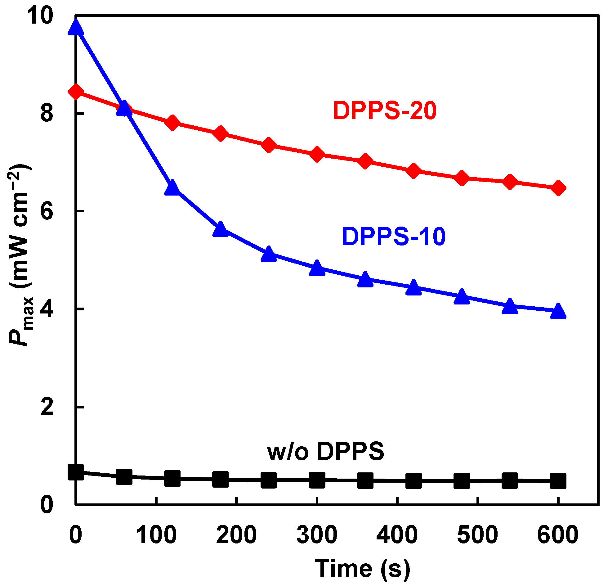
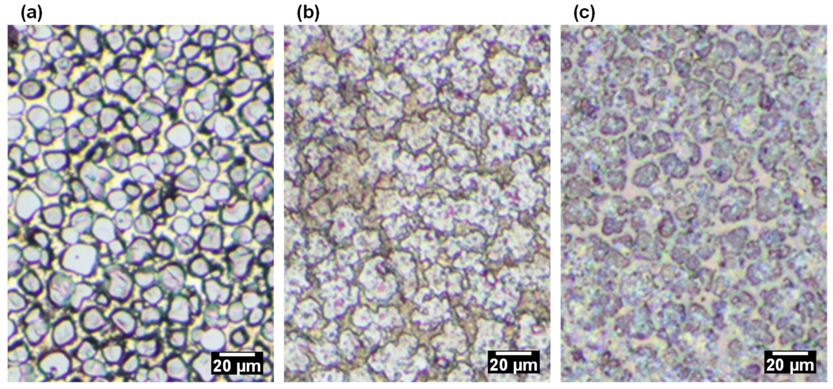
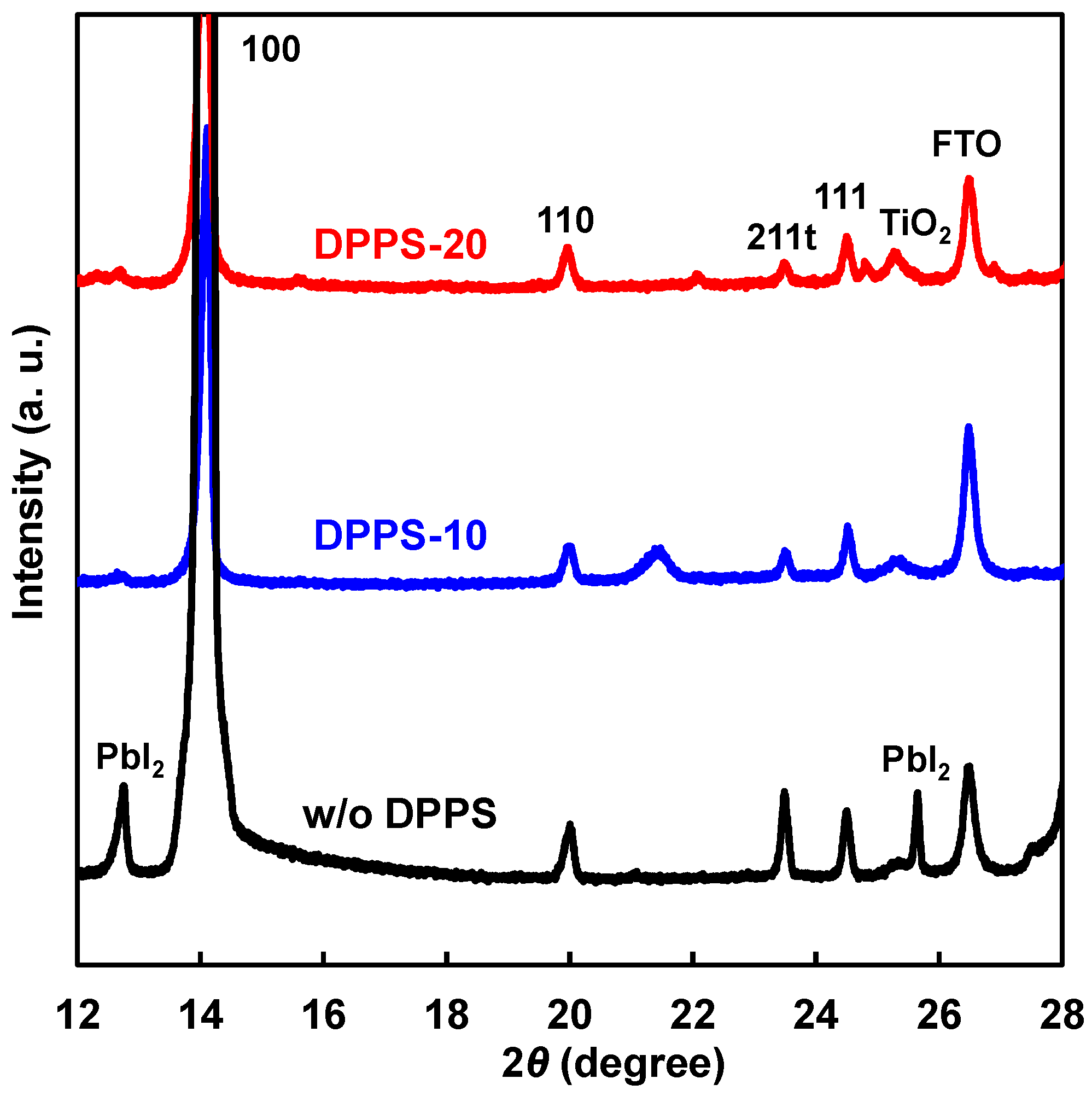
3. Results and Discussion
4. Conclusions
Author Contributions
Funding
Institutional Review Board Statement
Informed Consent Statement
Data Availability Statement
Conflicts of Interest
References
- Bati, A.S.R.; Zhong, Y.L.; Burn, P.L.; Nazeeruddin, M.K.; Shaw, P.E.; Batmunkh, M. Next-generation applications for integrated perovskite solar cells. Commun. Mater. 2023, 4, 2. [Google Scholar] [CrossRef]
- Vesce, L.; Stefanelli, M.; Rossi, F.; Castriotta, L.A.; Basosi, R.; Parisi, M.L.; Sinicropi, A.; Carlo, A.D. Perovskite solar cell technology scaling-up: Eco-efficient and industrially compatible sub-module manufacturing by fully ambient air slot-die/blade meniscus coating. Prog. Photovolt. 2024, 32, 115–129. [Google Scholar] [CrossRef]
- Yan, G.; Yuan, Y.; Kaba, M.; Kirchartz, T. Visualizing performances losses of perovskite solar cells and modules: From laboratory to industrial scales. Adv. Energy Mater. 2024, 15, 2403706. [Google Scholar] [CrossRef]
- Kim, H.J.; Kim, H.S.; Park, N.G. Progress of perovskite solar modules. Adv. Energy Sustain. Res. 2021, 2, 2000051. [Google Scholar] [CrossRef]
- Afroz, M.; Ratnesh, R.K.; Srivastava, S.; Singh, J. Perovskite solar cells: Progress, challenges, and future avenues to clean energy. Solar Energy 2025, 287, 113205. [Google Scholar] [CrossRef]
- Yu, X.; Sun, X.; Zhu, Z.; Li, Z.a. Stabilization strategies of buried interface for efficient SAM-based inverted perovskite solar cells. Angew. Chem. Int. Ed. 2025, 64, e202419608. [Google Scholar] [CrossRef] [PubMed]
- Ouedraogo, N.A.N.; Ouyang, Y.; Guo, B.; Xiao, Z.; Zuo, C.; Chen, K.; He, Z.; Odunmbaku, G.O.; Ma, Z.; Long, W.; et al. Printing perovskite solar cells in ambient air, A Review. Adv. Energy Mater. 2024, 14, 2401463. [Google Scholar] [CrossRef]
- Tian, R.; Zhou, S.; Meng, Y.; Liu, C.; Ge, Z. Material and device design of flexible perovskite solar cells for next-generation power supplies. Adv. Mater. 2024, 36, 2311473. [Google Scholar] [CrossRef]
- Nakka, L.; Cheng, Y.; Aberle, A.G.; Lin, F. Analytical Review of Spiro-OMeTAD Hole transport materials: Paths toward stable and efficient perovskite solar cells. Adv. Energy Sustain. Res. 2022, 3, 2200045. [Google Scholar] [CrossRef]
- Sajida, S.; Elseman, A.M.; Huang, H.; Ji, J.; Dou, S.; Jiang, H.; Liu, X.; Wei, D.; Cui, P.; Li, M. Breakthroughs in NiOx-HTMs towards stable, low-cost and efficient perovskite solar cells. Nano Energy 2018, 51, 408–424. [Google Scholar] [CrossRef]
- Duan, Y.; Chen, Y.; Wu, Y.; Liu, Z.; Liu, S.; Peng, Q. A comprehensive review of organic hole-transporting materials for highly efficient and stable inverted perovskite solar cells. Adv. Funct. Mater. 2024, 34, 2315604. [Google Scholar] [CrossRef]
- Zhou, H.; Wang, W.; Duan, Y.; Sun, R.; Li, Y.; Xie, Z.; Xu, D.; Wu, M.; Wang, Y.; Li, H.; et al. Glycol monomethyl ether-substituted carbazolyl hole-transporting material for stable inverted perovskite solar cells with efficiency of 25.52 %. Angew. Chem. Int. Ed. 2024, 63, e202403068. [Google Scholar] [CrossRef]
- Khan, D.; Liu, X.; Qu, G.; Nath, A.R.; Xie, P.; Xu, Z.X. Nexuses between the chemical design and performance of small molecule dopant-free hole transporting materials in perovskite solar cells. Small 2022, 19, 2205926. [Google Scholar] [CrossRef] [PubMed]
- Yamamoto, K.; Murakami, T.N. Thermal stability of perovskite solar cells incorporated with spiro-OMeTAD and an ionic liquid dopant. Jpn. J. Appl. Phys. 2024, 63, 02SP82. [Google Scholar] [CrossRef]
- Wang, S.; Huang, Z.; Wang, X.; Li, Y.; Günther, M.; Valenzuela, S.; Parikh, P.; Cabreros, A.; Xiong, W.; Meng, Y.S. Unveiling the role of tBP–LiTFSI complexes in perovskite solar cells. J. Am. Chem. Soc. 2018, 140, 16720–16730. [Google Scholar] [CrossRef]
- Shen, Y.; Deng, K.; Chen, Q.; Gao, G.; Li, L. Crowning lithium ions in hole-transport layer toward stable perovskite solar cells. Adv. Mater. 2022, 34, 2200978. [Google Scholar] [CrossRef]
- Habisreutinger, S.N.; Noel, N.K.; Snaith, H.J.; Nicholas, R.J. Investigating the role of 4-tert butylpyridine in perovskite solar cells. Adv. Energy Mater. 2017, 7, 1601079. [Google Scholar] [CrossRef]
- Li, Y.; Wang, Y.; Zhang, T.; Yoriya, S.; Kumnorkaew, P.; Chen, S.; Guo, X.; Zhao, Y. Li dopant induces moisture sensitive phase degradation of an all-inorganic CsPbI2Br perovskite. Chem. Commun. 2018, 54, 9809–9812. [Google Scholar] [CrossRef] [PubMed]
- Wan, Z.; Jiang, S.; Lu, H.; Zhu, J.; Wang, Y.; Zeng, H.; Yin, H.; Wei, R.; Luo, J.; Jia, C. Replacing Li+ in Li-TFSI with a benzene ring: Constructing non-ionic p-dopants for stable and efficient perovskite solar cells. J. Mater. Chem. C 2024, 12, 8078–8086. [Google Scholar] [CrossRef]
- Yin, H.; Wan, Z.; Zhu, J.; Xia, J.; Azam, M.; Yang, H.; Zeng, H.; Wei, R.; Wang, Y.; Luo, J.; et al. Anionic engineering of a p-dopant enables efficient and stable perovskite solar cells. J. Mater. Chem. A 2024, 12, 28943–28952. [Google Scholar] [CrossRef]
- Petrulevicius, J.; Yang, Y.; Liu, C.; Steponaitis, M.; Kamarauskas, E.; Daskeviciene, M.; Bati, A.S.R.; Malinauskas, T.; Jankauskas, V.; Rakstys, K.; et al. Asymmetric triphenylethylene-based hole transporting materials for highly efficient perovskite solar cells. ACS Appl. Mater. Interfaces 2024, 16, 7310–7316. [Google Scholar] [CrossRef] [PubMed]
- Akram, W.; Zahid, W.A.; Abdelmohsen, S.A.M.; Alanazi, M.M.; Hossain, I.; Elmushyakhi, A.; Iqbal, J. Tailoring electronic structure and charge transport in thiophene-based hole transport materials: An end-capping acceptor strategy for efficient perovskite solar cells. J. Phys. Chem. Solids 2023, 182, 111596. [Google Scholar] [CrossRef]
- Li, W.; Zhao, W.; Lia, K.; Han, X. A review on conventional perovskite solar cells with organic dopant-free hole-transport materials: Roles of chemical structures and interfacial materials in efficient devices. J. Mater. Chem. C 2024, 12, 1147–1176. [Google Scholar] [CrossRef]
- Xie, G.; Wang, J.; Yin, S.; Liang, A.; Wang, W.; Chen, Z.; Feng, C.; Yu, J.; Liao, X.; Fu, Y.; et al. Dual-strategy tailoring molecular structures of dopant-free hole transport materials for efficient and stable perovskite solar cells. Angew. Chem. Int. Ed. 2024, 63, e202403083. [Google Scholar] [CrossRef]
- Duan, C.; Zou, F.; Li, S.; Zhu, Q.; Li, J.; Chen, H.; Zhang, Z.; Chen, C.; Guo, H.; Qiu, J.; et al. Dopant-free starlike molecular hole conductor with ordered packing for durable all-inorganic perovskite solar cells. Adv. Energy Mater. 2024, 14, 2303997. [Google Scholar] [CrossRef]
- Tan, J.; Zhang, J.; Sun, H.; Chen, K.; Gao, X.; Zhang, P.; Zhong, C.; Wu, F.; Li, Z.; Zhu, L. Dopant-free hole transport material based on non-covalent interaction for efficient perovskite solar cells. Small 2024, 20, 2407027. [Google Scholar] [CrossRef]
- Taguchi, M.; Suzuki, A.; Oku, T.; Ueoka, N.; Minami, S.; Okita, M. Effects of annealing temperature on decaphenylcyclopentasilane-inserted CH3NH3PbI3 perovskite solar cells. Chem. Phys. Lett. 2019, 737, 136822. [Google Scholar] [CrossRef]
- Oku, T.; Taguchi, M.; Suzuki, A.; Kitagawa, K.; Asakawa, Y.; Yoshida, S.; Okita, M.; Minami, S.; Fukunishi, S.; Tachikawa, T. Effects of polysilane addition to chlorobenzene and high temperature annealing on CH3NH3PbI3 perovskite photovoltaic devices. Coatings 2021, 11, 665. [Google Scholar] [CrossRef]
- Kuroyanagi, K.; Oku, T.; Ono, I.; Okumura, R.; Enomoto, A.; Suzuki, A.; Fukunishi, S.; Tachikawa, T.; Hasegawa, T. Effects of guanidinium iodide surface treatment on CH3NH3PbI3 perovskite solar cells with added decaphenylcyclopentasilane. Nano Trends 2024, 5, 100030. [Google Scholar] [CrossRef]
- Ono, I.; Oku, T.; Genko, Y.; Okumura, R.; Nasu, T.; Mizuno, S.; Tachikawa, T.; Hasegawa, T.; Fukunishi, S. Stable decaphenylcyclopentasilane hole transport layers for double-stacked perovskite photovoltaic devices fabricated under ambient atmosphere. Chem. Inorg. Mater. 2024, 4, 100066. [Google Scholar] [CrossRef]
- Oku, T. Crystal structures of perovskite halide compounds used for solar cells. Rev. Adv. Mater. Sci. 2020, 59, 264–305. [Google Scholar] [CrossRef]
- Zhao, R.; Wu, T.; Hua, Y.; Wang, Y. Improving performance of perovskite solar cells enabled by defects passivation and carrier transport dynamics regulation via organic additive. Chin. Chem. Lett. 2025, 36, 109587. [Google Scholar] [CrossRef]
- Pu, X.; Cao, Q.; He, X.; Su, J.; Wang, W.; Zhang, X.; Wang, D.; Zhang, Y.; Yang, J.; Wang, T.; et al. Synergistic crystallization kinetics modulation and deep/shallow level defect passivation via an organometallic cobaltocenium salt toward high-performance inverted perovskite solar cells. Adv. Energy Mater. 2024, 14, 2303972. [Google Scholar] [CrossRef]
- Wang, H.; Zheng, Y.; Zhang, G.; Wang, P.; Sui, X.; Yuan, H.; Shi, Y.; Zhang, G.; Ding, G.; Li, Y.; et al. In situ dual-interface passivation strategy enables the efficiency of formamidinium perovskite solar cells over 25%. Adv. Mater. 2024, 36, 2307855. [Google Scholar] [CrossRef] [PubMed]
- He, Z.; Luan, T.; Zhang, S.; Wei, Q.; Huang, D.; Wang, L.; Wang, Y.; Li, P.; Yu, W.W. Robust imidazole-linked covalent organic framework enabling crystallization regulation and bulk defect passivation for highly efficient and stable perovskite solar cells. Adv. Mater. 2024, 36, 2410363. [Google Scholar] [CrossRef] [PubMed]

| Devices | Time (Day) | JSC (mA cm−2) | VOC (V) | FF | Rs (Ω cm2) | Rsh (Ω cm2) | η (%) | ηave (%) |
|---|---|---|---|---|---|---|---|---|
| w/o DPPS | 0 | 13.5 | 0.246 | 0.275 | 2.2 | 21 | 0.91 | 0.70 |
| DPPS-10 | 0 | 19.8 | 0.658 | 0.414 | 16.8 | 648 | 5.40 | 3.96 |
| DPPS-20 | 0 | 20.4 | 0.682 | 0.477 | 15.3 | 1427 | 6.63 | 2.88 |
| w/o DPPS | 13 | 7.9 | 0.209 | 0.270 | 4.4 | 29 | 0.45 | 0.37 |
| DPPS-10 | 60 | 20.4 | 0.739 | 0.545 | 5.4 | 582 | 8.22 | 6.29 |
| DPPS-20 | 60 | 20.4 | 0.759 | 0.566 | 11.6 | 1450 | 8.77 | 4.36 |
| w/o DPPS | 351 | 13.9 | 0.245 | 0.260 | 8.3 | 19 | 0.884 | 0.621 |
| DPPS-10 | 448 | 21.2 | 0.729 | 0.596 | 4.6 | 570 | 9.24 | 7.02 |
| DPPS-20 | 448 | 20.8 | 0.719 | 0.639 | 2.6 | 317 | 9.57 | 4.29 |
Disclaimer/Publisher’s Note: The statements, opinions and data contained in all publications are solely those of the individual author(s) and contributor(s) and not of MDPI and/or the editor(s). MDPI and/or the editor(s) disclaim responsibility for any injury to people or property resulting from any ideas, methods, instructions or products referred to in the content. |
© 2025 by the authors. Licensee MDPI, Basel, Switzerland. This article is an open access article distributed under the terms and conditions of the Creative Commons Attribution (CC BY) license (https://creativecommons.org/licenses/by/4.0/).
Share and Cite
Kuroyanagi, K.; Oku, T.; Ono, I.; Shimada, H.; Suzuki, A.; Tachikawa, T.; Fukunishi, S. Fabrication and Characterization of CH3NH3PbI3 Perovskite Photovoltaic Devices with Decaphenylcyclopentasilane Hole Transport Layers. Coatings 2025, 15, 253. https://doi.org/10.3390/coatings15030253
Kuroyanagi K, Oku T, Ono I, Shimada H, Suzuki A, Tachikawa T, Fukunishi S. Fabrication and Characterization of CH3NH3PbI3 Perovskite Photovoltaic Devices with Decaphenylcyclopentasilane Hole Transport Layers. Coatings. 2025; 15(3):253. https://doi.org/10.3390/coatings15030253
Chicago/Turabian StyleKuroyanagi, Keisuke, Takeo Oku, Iori Ono, Haruto Shimada, Atsushi Suzuki, Tomoharu Tachikawa, and Sakiko Fukunishi. 2025. "Fabrication and Characterization of CH3NH3PbI3 Perovskite Photovoltaic Devices with Decaphenylcyclopentasilane Hole Transport Layers" Coatings 15, no. 3: 253. https://doi.org/10.3390/coatings15030253
APA StyleKuroyanagi, K., Oku, T., Ono, I., Shimada, H., Suzuki, A., Tachikawa, T., & Fukunishi, S. (2025). Fabrication and Characterization of CH3NH3PbI3 Perovskite Photovoltaic Devices with Decaphenylcyclopentasilane Hole Transport Layers. Coatings, 15(3), 253. https://doi.org/10.3390/coatings15030253