1. Introduction
Recently, the world has been facing remarkable development of solar power technology. The share of global energy generation from solar photovoltaics rose up from only 1.1% to 5.5% in 2023 [
1,
2]. While photovoltaics shows significant promise in answering the growing needs of worldwide energy, there remain significant challenges in meeting the already set high targets. One promising solar technology is perovskite solar cells (PSCs) [
3,
4]. This is due to the incredibly rapid progress in the development of these structures in terms of their efficiency, increasing from about 3.8% in 2009 to about 26.1% in 2023 [
5]. Other advantages of the PSC technology are optically high absorption characteristics over a wide spectrum, direct bandgap, a high absorption coefficient, balanced charge transport with long diffusion lengths, defect tolerance and high carrier mobility and lifetime [
6,
7,
8,
9,
10]. The standard device structure of PSC contains an absorbing layer, an electron transport layer (ETL), a hole transport layer (HTL), a transparent conductive oxide (anode) and a metal contact (cathode). Currently, the most widely used ETL is titanium dioxide (TiO
2) because of its superior stability. However, the fact that it requires a high annealing temperature and favors the ion migration process, leading to cell degradation, necessitates finding an alternative. Suitable replacements to TiO
2 are ZnO, CdS, PCBM and SnO
2 [
11,
12,
13].
In this work, we present an electron transport layer using binary wide bandgap oxides with appropriate optical and electrical parameters for efficient hybrid perovskite solar cells with improved stability and performance. We use zinc–tin oxide as the ETL, since it has a negligible effect on the transmittance of the incident light, regardless of its thickness, so that the thickest compact layer efficiently blocks the back electron transfer. We have decided to use this ETL, as there are recent attempts that show enhanced performance by modifying the ETL layer using ZTO [
14,
15]. In terms of stability and efficiency improvements, ternary metal layers on the basis of Zn–Sn–O yield better results compared to the standard TiO
2 layers [
16]. Furthermore, ZTO is an inexpensive material, and there are various production methods that can be applied from traditional vacuum deposition techniques such as RF magnetron sputtering to solution-processed deposition techniques such as spin coating. We have decided to use the latter, which is a chemical method to create uniform thin layer [
17]. This method has the benefit of reduced production cost, large area coverage and high throughput.
Our aim is to improve working parameters of PSC devices by enhancing electron extraction through reduction of the energy barrier at the perovskite/ETL interface and improved photoelectron transfer from the perovskite-absorbing layer to the new ETL layer. By varying the ratio of the metal components zinc oxide to tin oxide in the created solution, we obtained several different compounds and analyzed their properties. The interval of the ratio is specified from 0.40 to 0.90, because the boundary cases near 0 and 1 have been extensively researched previously, and it is not possible to control the electrophysical properties of the material in those boundary cases. Then, we measure the characteristics of the spin-coated samples—surface morphology, optical reflection, work function, X-ray photoelectron spectroscopy and X-ray diffraction.
2. Materials and Methods
The solutions were prepared for spin coating of the films onto glass substrates as follows:
The 0.2 M solution (1.36 g) of Zn(II) chloride (ZnCl
2) (Merck) (for syntheses) and 0.2 M solution (3.50 g) Tin(IV) chloride pentahydrate, 98+% (SnCl
4.5H
2O) extra pure Acros Organics in 50 mL isopropyl alcohol (for analysis) (Merck) were prepared. From these, 3 mL solutions, both with pure zinc chloride and tin chloride pentahydrate, as well as with different ratios of zinc and tin, were prepared (
Table 1).
The working volume was 30 μL, dispensed onto the rotating sample with a size of 15 mm × 20 mm for 30 s at rotation speed 3500 min−1. The as-deposited films were dried at 100 °C for 1 h and afterwards were annealed at 400 °C in a tube furnace at ambient conditions. To form thick layers, the deposition was repeated several times, followed in every case by drying and annealing.
For measuring the V/A characteristics of the metal electrodes from aluminum, Kurt J.Lesket, 99.999% pure and calcium, Kurt J.Lesket, 99% were deposited by thermal evaporation in vacuum onto films prepared by spin coatings. The thickness of the metal layers was about 200 nm.
Table 1 shows the values of the material composition x in (ZnO)
x(SnO
2)
1−x (0 < x < 1).
The DSC (Differential Scanning Calorimetry) measurements were performed with a Differential Scanning Calorimetry apparatus, NETZSCH DSC 200 PC. The results were evaluated with the standard NETZSCH Proteus Thermal Analysis software version 4.3.1. A certain amount of the powder test material was placed in a crucible. The crucible was covered by lid with a small hole and was closed using a DSC sample preparation press. The masses of samples, crucibles and lids were weighed. The powders are hygroscopic, and the preparation of the samples is carried out in the shortest possible time. The closed capsule is shaken for initial homogenization. The mixture in the capsule is homogenized after the formation of a liquid phase upon heating. The lids with a hole limit the possibility of moisture entering the capsule but allow volatile components to escape. The prepared sample was placed in the furnace of the DSC apparatus. Besides the capsule with the test sample, an empty sample (empty crucible with a lid) was placed on the second thermocouple, which served as a reference sample to account for the influence of the heat capacity of the crucibles. Nitrogen was used as a protective to purge gases. The gas flow rate was 20 mL/min. The temperature range for heating and cooling was chosen from 20 °C to 500 °C. The heating and cooling rates were both equal to 6 °C/min. The analysis was performed on metal Al capsules, and the quantity of the samples was weighted in analytical balance with an accuracy ±0.02 mg.
The X-ray photoelectron spectroscopy (XPS) studies were performed on a VG Escalab MKII electron spectrometer using achromatic AlKα radiation with energy of 1486.6 eV under base pressure 10−8 Pa and a total instrumental resolution of 1 eV. The binding energies (BEs) were determined utilizing the C1s line as a reference with an energy of 285 eV. The accuracy of the measured BE was 0.2 eV. The O1s photoelectron spectra were subjected to an additional fitting procedure with software XPSPEAK4.1.
XRD X-ray diffraction (XRD) measurements were performed using an AXS D8 Advance diffractometer with reflection θ/2θ geometry, Cu Kα radiation, receiving slit 0.2 mm, scintillation counter, 40 mA, 40 kV from Bruker Inc. (Karlsruhe, Germany). The analysis of the XRD patterns was carried out with the PowderCell program [
18], and quantitative Rietveld analysis of the data was performed using the program Fullprof [
19].
The total transmittance of the samples was measured with a Jasco V-670 UV–Vis–NIR spectrophotometer equipped with an integrating sphere in the spectral range 250–1500 nm. The optical direct bandgap was determined using the Kubelka–Munk theory. The surface morphology of the prepared samples was studied using a high-resolution scanning electron microscope (HR-SEM Zeiss Merlin ULTRA 55) at an accelerating voltage of 1.74 kV. The thickness was determined from SEM cross-section images.
Work function measurements were performed on a Scanning Kelvin Probe microscope SKP5050 (KP Technology, Wick, Scotland) with a resolution of 1–3 meV—PC-controlled with dedicated software for all parameters, off—null with parasitic capacity rejection and 3D map of surface potential visualization. Volt amperometric characterizations were performed with a FHI/ELAB 050-891 Potentiostat at a scan rate of 100 mV/s within the limit of ±3 V.
3. Results and Discussion
3.1. DSC Analysis
Samples with different ratios of zinc chloride to stannous chloride were tested. The mass of the components and the total mass of the sample were weighed. The mole ratios of the components were calculated, and the data are presented in
Table 2.
Figure 1 shows the graphs from the DSC measurement of five samples. The concentration ratio in moles between Zn and Sn decreases from top to bottom. An indicator for a given process is the temperature value of the peak that is registered during the measurement. ZnCl
2 and SnCl
4 are hygroscopic and form crystal hydrates. Upon heating, SnCl
4.5H
2O melts; after which, the water molecules are redistributed between ZnCl
2 and SnCl
4 in new crystal hydrate structures. This explains the presence of the three identical peaks with temperatures around 58 °C, 67 °C and 76 °C in the samples containing both substances.
In all the samples, the presence of an exothermic reaction was recorded in a range from 50 °C to 150 °C. Its probable cause is the formation of complex compounds of Zn, Sn, water, hydrochloric acid and hypochlorous acid. Zn(OH)Cl.nH
2O and Sn(OH)
2Cl
2.nH
2O are formed [
20,
21,
22]. In the pure ZnCl
2 and SnCl
4.5H
2O samples, only one peak was observed at 138 °C and 70 °C, respectively. In the case of the mixed samples, it can be seen that the course of these processes is influenced by the size of the crystal fractions of the two substances.
In all the samples, the presence of an endothermic reaction was recorded in the range from 150 °C to 250 °C. Its probable cause is the cascade dehydration of the compounds formed. Water evaporates, and Zn(OH)Cl and Sn(OH)
2Cl
2 remain. Sample E contains only SnCl
4.5H
2O, showing the exothermic reaction started at 267 °C, had a maximum at 270 °C and ended at 287 °C. This process is probably the decomposition of Sn(OH)
2Cl
2 to SnO
2 and HCl, and hydrogen chloride is evaporated.
A clearly defined exothermic reaction in Sample E is registered as heating continues. It starts at 420.1 °C, has a maximum at 437.8 °C and ends at 451.9 °C. This reaction indicates the formation of a stable structure.
The endothermic peak at 317 °C for sample A can be explained by the melting of anhydrous ZnCl2. The endothermic peak at 294 °C for sample B can be explained by a lowering of the melting temperature of anhydrous ZnCl2 mixed with the tin compounds.
Sample A contains only ZnCl
2, showing a clearly defined exothermic reaction is registered as heating continues. It starts at 367.7 °C, has a maximum at 379.2 °C and ends at 407 °C. This reaction indicates the formation of a stable structure. Zinc is oxidized, and zinc oxide is formed.
These are the processes describing the decomposition of Zn(OH)Cl to ZnO and HCl by evaporating HCl [
20,
23,
24]. As is stated in [
24], the reaction (2) could take place at lower temperatures provoked by a hygroscopic effect, as seen in our case as well.
In the mixed samples, the two decomposition reactions of Zn(OH)Cl and Sn(OH)
2Cl
2 occur together in the capsules. In the temperature range from 250 °C to 500 °C, not two independent peaks are observed but only one. This shows that a combined process takes place with the participation of both Zn and Sn compounds. The ZnO formation process is facilitated by the already started SnO
2 formation process. As the tin concentration increases, the temperature of the exothermic reaction to form ZnO decreases. This happens until the temperature at which the decomposition of Sn(OH)
2Cl
2 starts is reached; after which, the temperature does not change. The tin atoms are embedded in the atomic lattice of ZnO. The end result of this is that ZnO doped with tin is obtained. The detailed explanation is given in
Section 3.6.
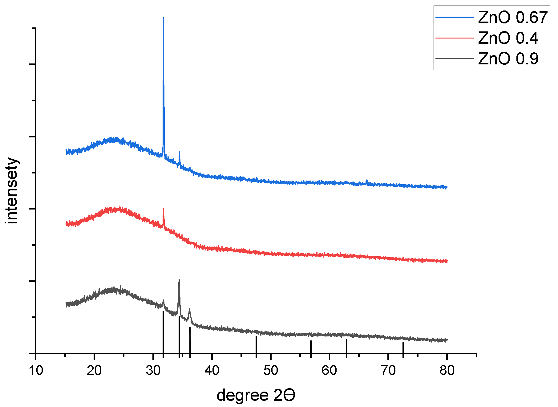
3.2. XRD Analysis
Figure 2 shows the spectra of X-ray diffractometry (XRD) of samples of (ZnO)
x(SnO
2)
1−x for x = 0.90, 0.67 and 0.40, respectively. For the case of ZnO-rich sample x = 0.90, the spectra definitely indicate a single-phase structure of zincite [
25,
26] with a grain size near 42 nm and preferable orientation in the (002) direction. The lattice constants are a = 3.26 Å and c = 5.21 Å, respectively.
For the sample with lower x = 0.67, the structure of the thin film is again on the same crystal system (hexagonal ZnO, but the preferred orientation changes to (100), lattice constants a = 3.25 Å and c = 5.198 Å, while the specific grain size rises sharply to nearly 181 nm. For samples with the lowest zinc content (x = 0.40), the crystal system is the same for zincite (a= 3.25 Å; c = 5.21 Å), with a grain size nearly 103 nm and orientation (001).
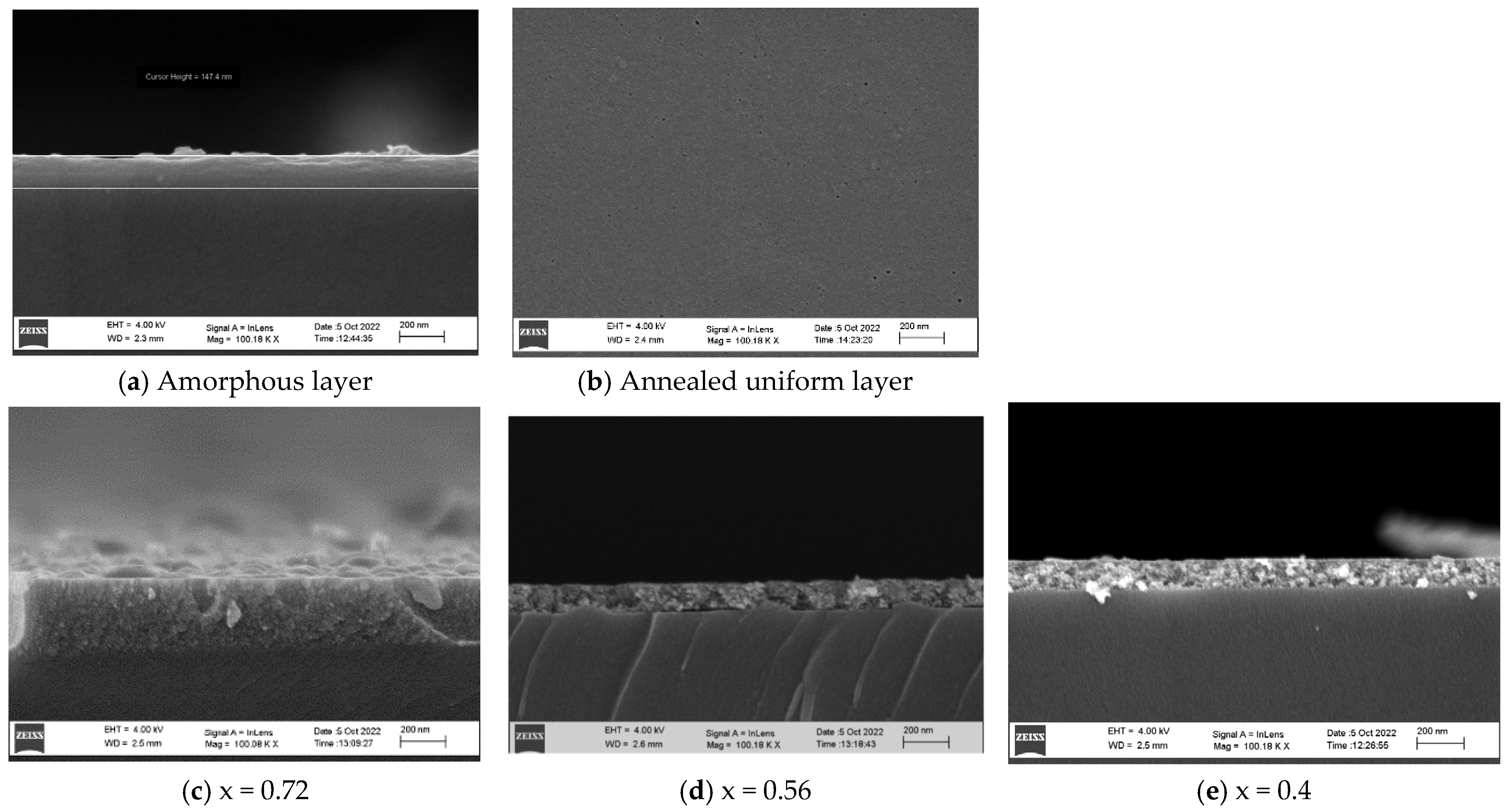
3.3. SEM Investigations
Figure 3 presents SEM micrographs of samples (ZnO)
x(SnO
2)
1−x with different x. The thickness of the layers depends proportionally on the number of the spin coatings and concentration of the precursors [
27,
28], as the deposited layers are amorphous (
Figure 3a) and need thermal treatment for crystallization. As the deposited layers were annealed at 400 °C in air for 2 h, after switching off the treatment, they were left for cooling down. The annealed layers were uniform, compact and dense (
Figure 3b). The thickness of the investigated layers varied between 30 and 300 nm. The observed grain sizes were 10–20 nm, and there were no voids, cracks or holes (
Figure 3c–e).
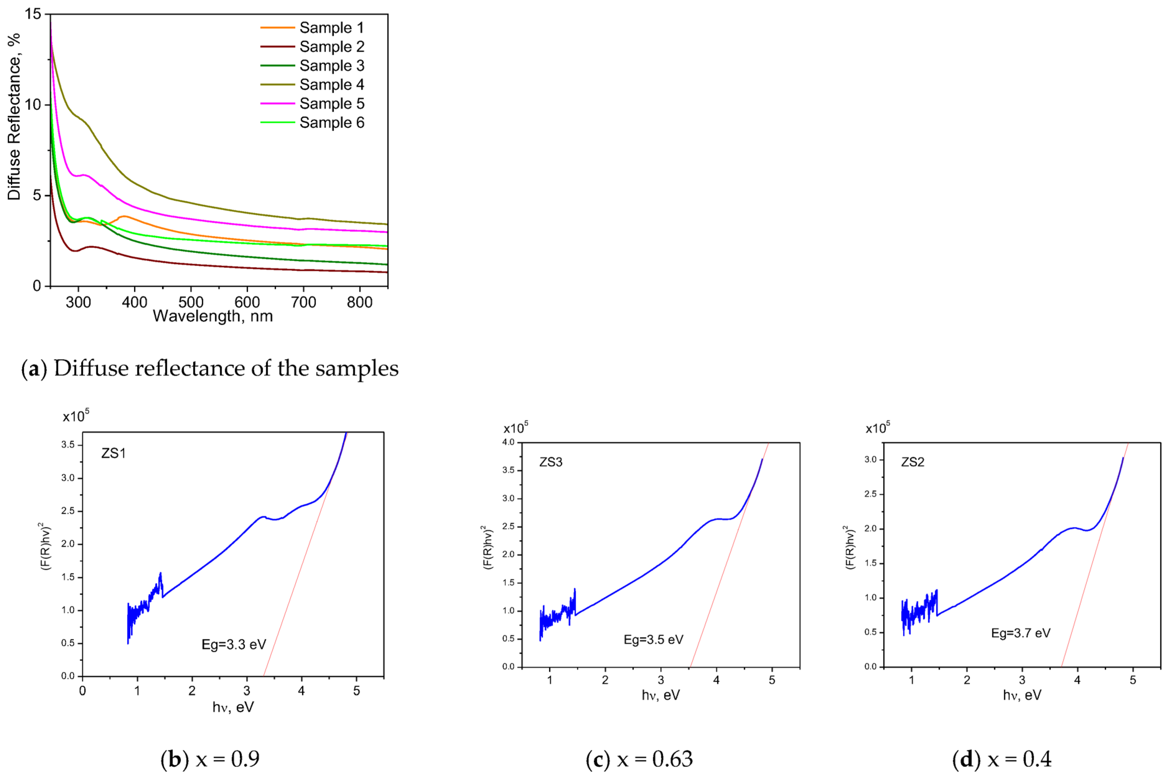
3.4. UV–Vis Spectrometry
Optical spectroscopy of the films was recorded using the UV–Vis–NIR spectrophotometer Jasco V-670 equipped with an integrating sphere in
Figure 4.
For calculation of the optical bandgap, the Kubelka–Munk theory was used:
where F(R) is the Kubelka–Munk function, and R is the diffuse reflectance. We plot (F(R)hv/t) (as the ordinate) versus hv (as the abscissa) in
Table 3. The place where the extrapolation of the straight line crosses the abscissa gives the value of the optical bandgap.
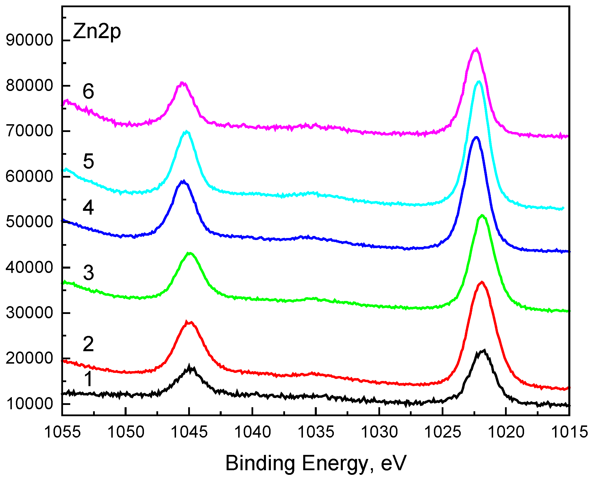
3.5. XPS Analysis
XPS analysis was performed to explore the chemical states of the elements over the surface of (ZnO)x(SnO2)1−x thin films. The following XPS parameters were recorded: C1s, O1s, Zn2p, Sn3d and Sn3p.
The high resolution of the Zn2p spectrum (
Figure 5) shows two peaks: Zn2p
3/2 and Zn2p
1/2 separated by 23.1 eV. This value is typical for Zn
2+ in ZnO.
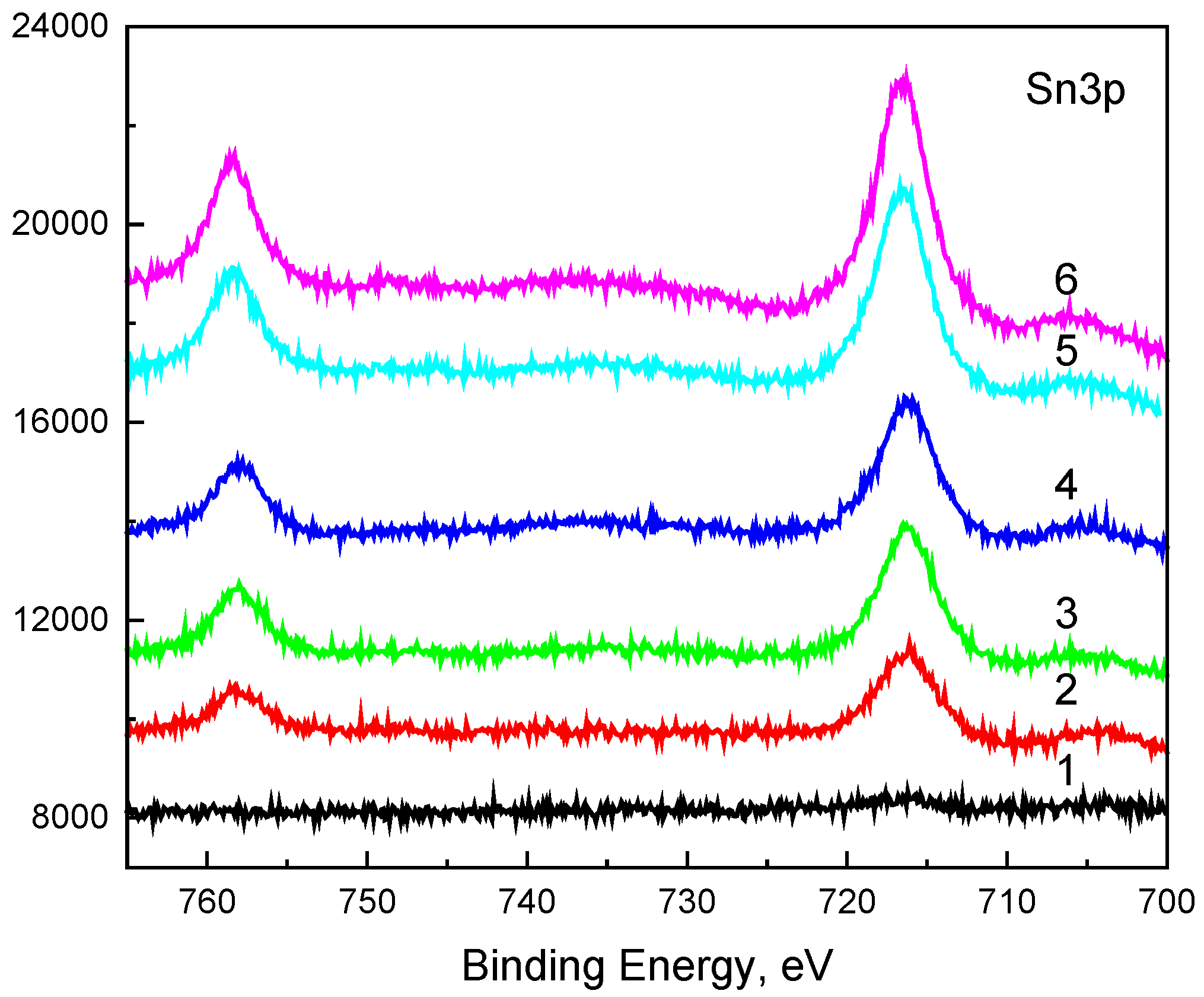
Figure 6 shows the Sn3p high-resolution spectra. The binding energies of the peaks and the shape of the spectra are typical for Sn
4+.
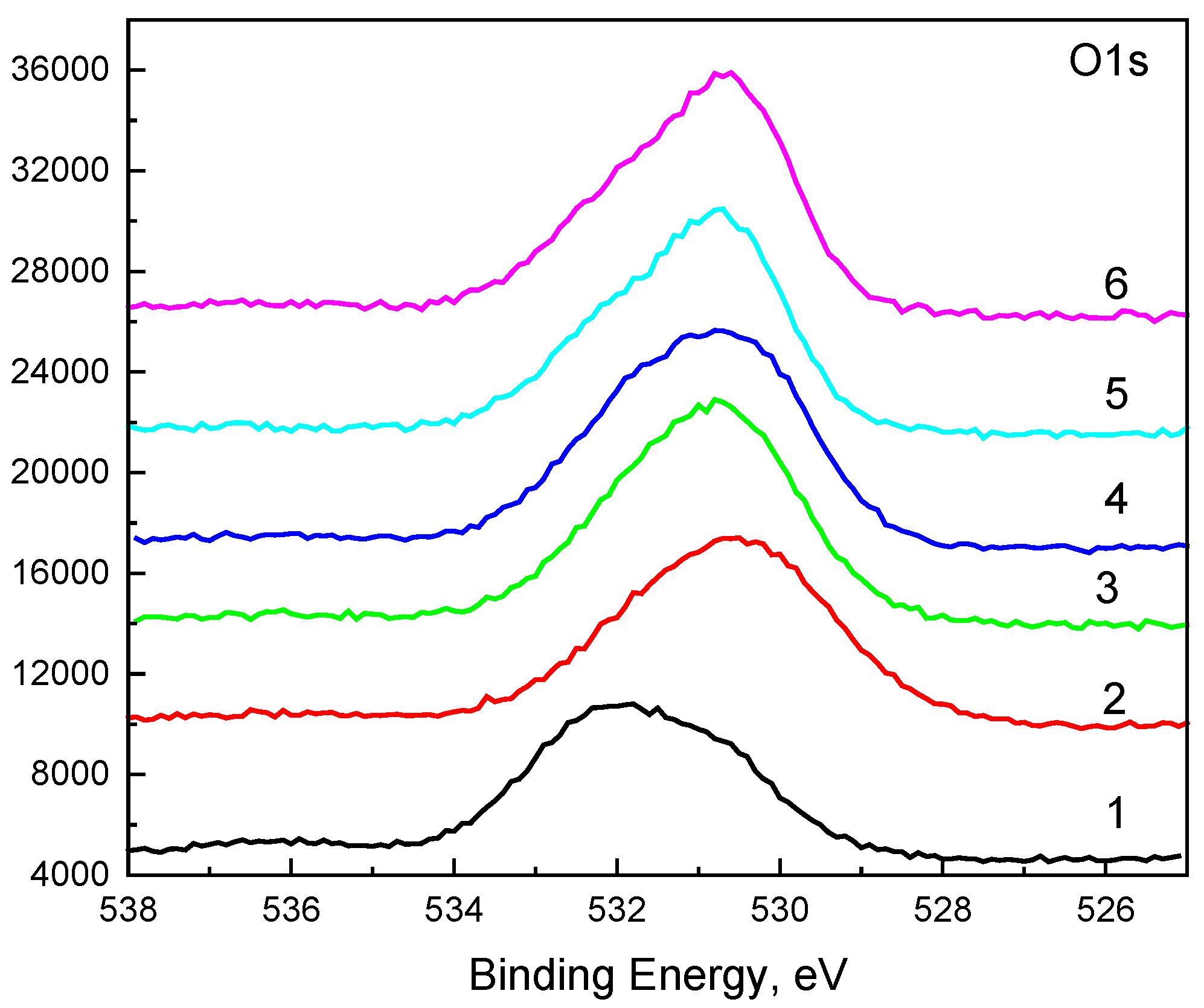
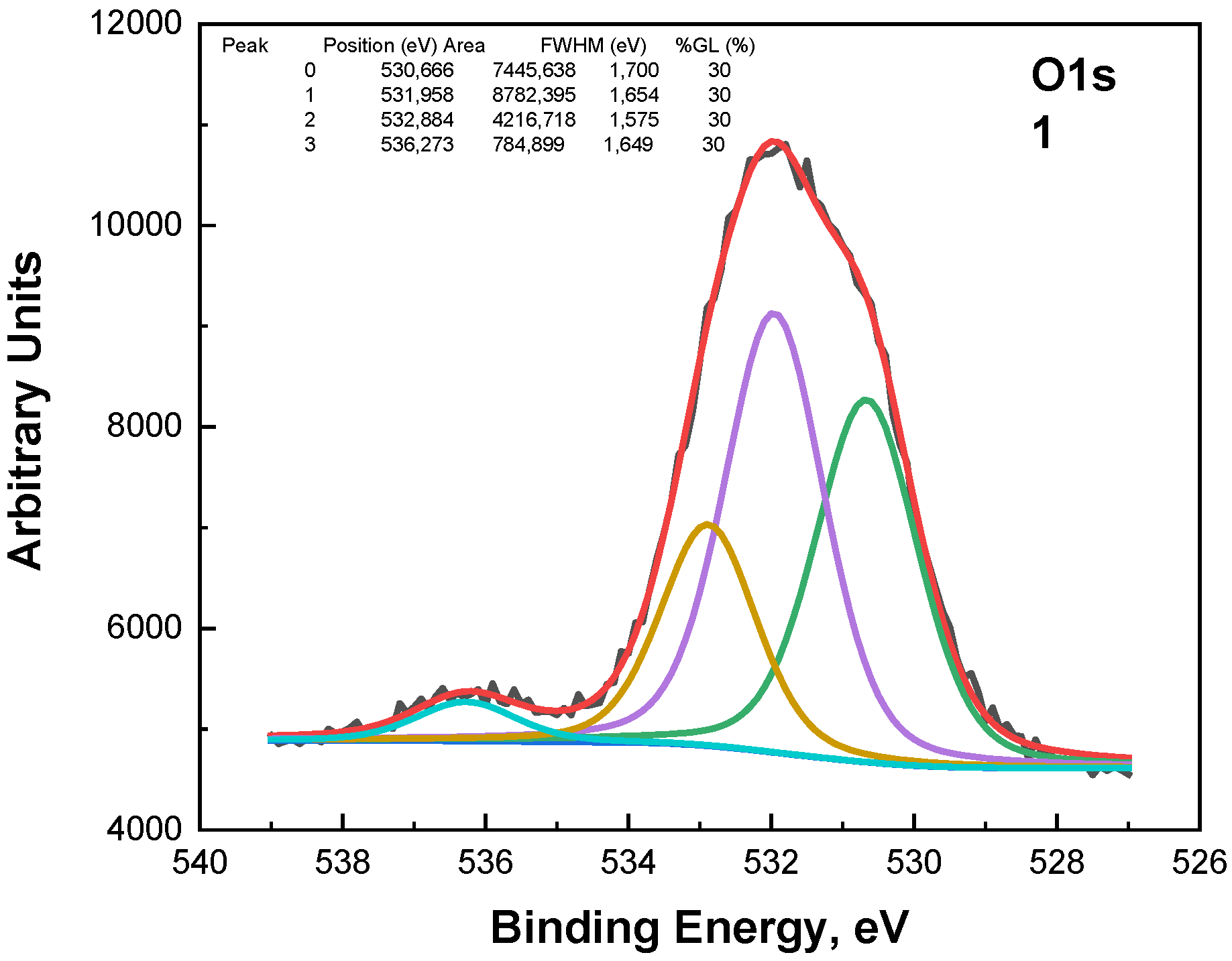
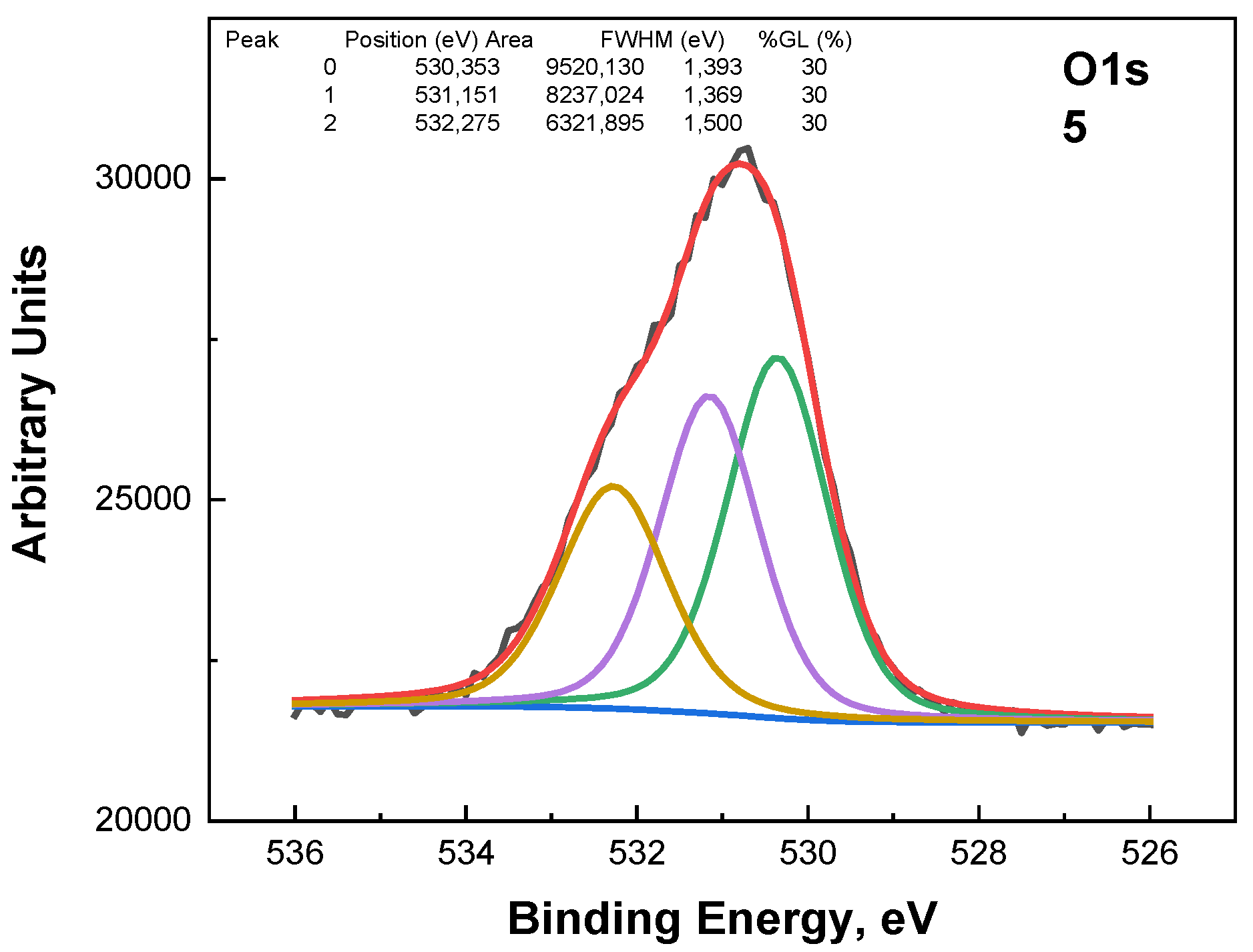
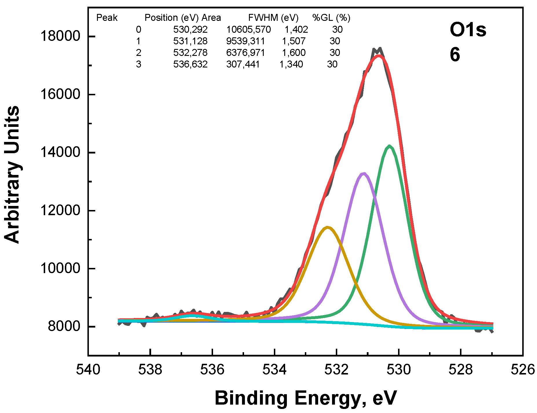
The O1s photoelectron spectra in
Figure 7 were subjected to the fitting procedure and are shown below. Three peaks were used for the fitting (
Figure 7,
Figure 8 and
Figure 9). The first peak at around 530.3 eV comes from the Sn-O bond or belongs to ZnO. The second peak at around 531.1 eV could be due to a vacancy in the ZnO lattice. A high binding energy in the O1s peak at ~532.3 eV is attributed to the chemisorbed oxygen over the surface of the ZnO-SnO
2 thin films.
A comparison of the ratio between peaks at 530.3 eV and 531.1 eV shows an interesting dependence on the composition (
Figure 10)—the concentration of vacancies in the wurtzite structure decreases, while the concentration of tin in the layers increases, respectively, when the concentration of zinc decreases. The peak at around 536 eV is due to Auger Na.
Figure 11 shows a data plot for all the samples. The values for the valence band energies are extracted by interpolation of the curves to their corresponding baselines and are summarized in
Table 4.
3.6. Work Function and I–V Measurements
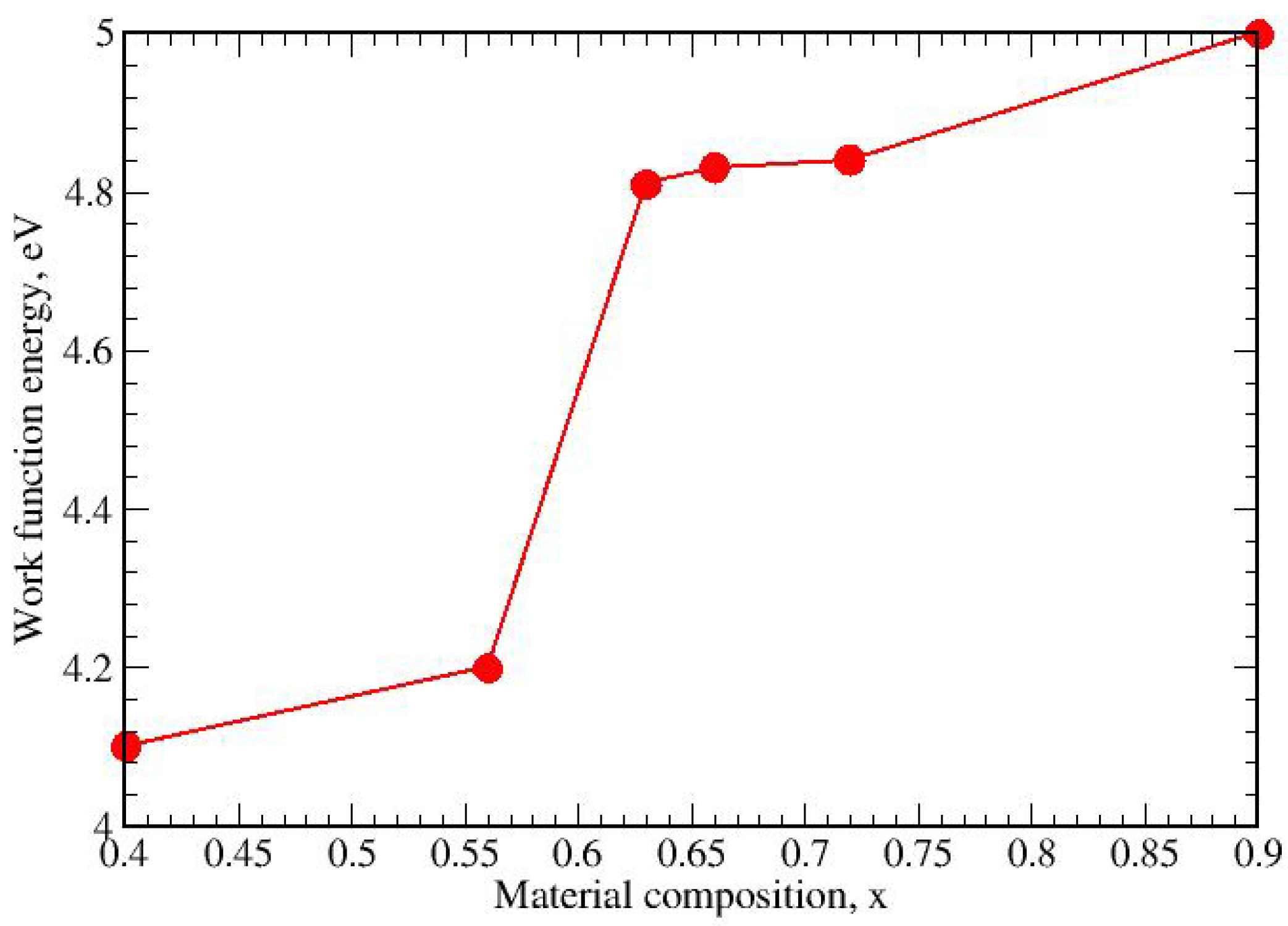
Figure 12 shows the dependence of the work function on the composition x of the deposited layers (ZnO)
x(SnO
2)
1−x. The value of the WF generally increases with x for 0.40 < x < 0.90. A step-like increase from 4.2 eV to 4.8 eV is observed in the narrow range of 0.56 < x < 0.66. This effect can be explained by the structure of the resulting layers expressed by a change in the orientation (texture) from {001} for x = 0.40 to {002} for x = 0.90 [
28].
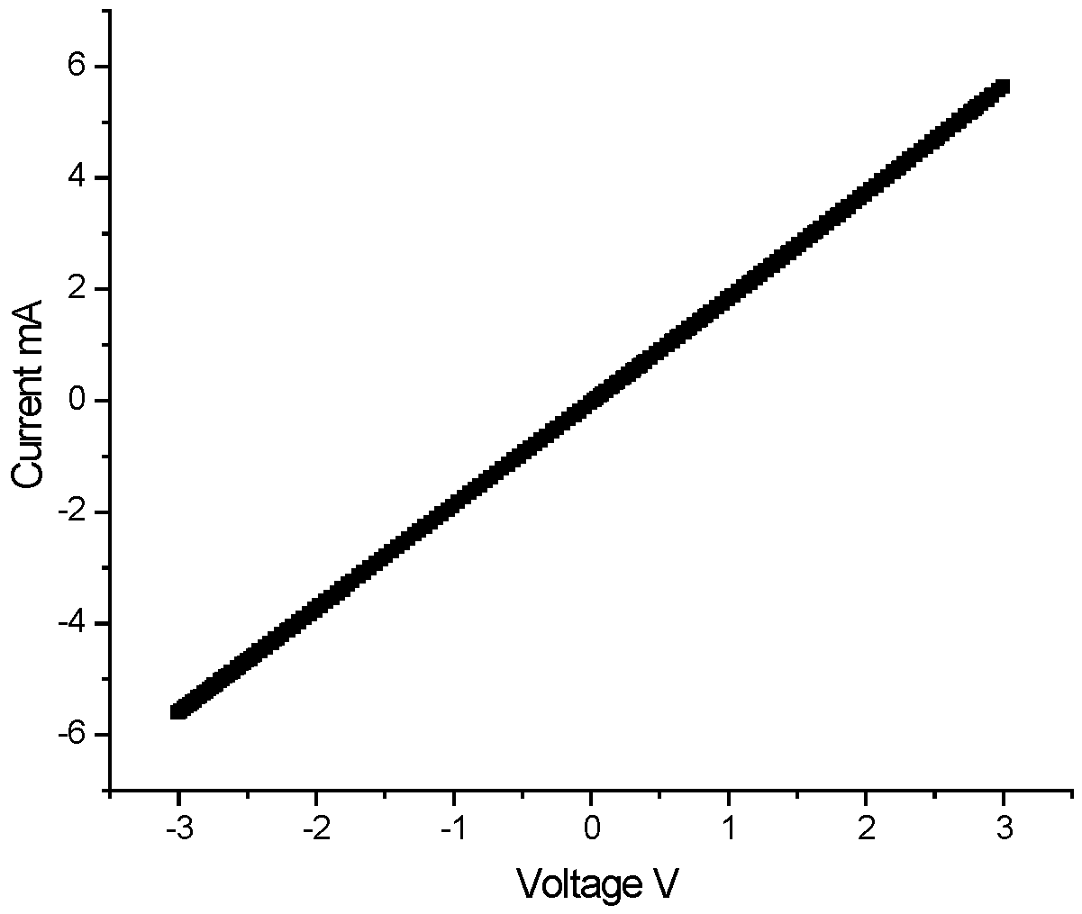
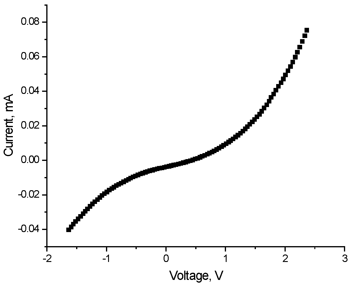
I–V measurements were made from thin-film heterostructures ITO/(ZnO)x(SnO2)1−x/Al for different compositions 0.40 < x < 0.90. For the values of x between 0.90 and 0.63, a linear dependence of the current on the applied voltage is observed.
The I–V characteristics in
Figure 13 can be explained by the difference between the work functions of the contact layers (WF
Al = 4.3 eV, WF
ITO = 4.84 eV) and the measured work function of the investigated semiconductor layer WF
semi = 4.84 eV.
The difference between the work functions varies with the tin content, and for example, at composition x = 0.56, a decrease in the work function of the (ZnO)
x(SnO
2)
1−x layer to 4.2 eV is observed (see
Figure 14). In this case, a formation of a barrier transition between the layer and the bottom contact ITO (WF
ITO = 5.0 eV) is observed.
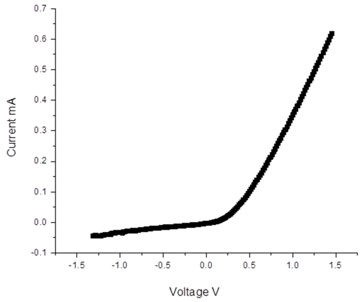
Due to a further increase in the tin content and, respectively, a decrease in the zinc content x, the work function of the (ZnO)
0.4(SnO
2)
0.6 layer drops to 4.1 eV. In this case, a back-to-back Schottky diode is formed. This behavior is explained by considering the values of the work function for the individual components. When a metal is in contact with an n-type semiconductor with a higher work function than that of the metal, a barrier contact is formed [
29]. For aluminum, this value is 4.3 eV, and for the deposited layer (ZnO)
0.4(SnO
2)
0.6, it is 4.1 eV, and in the negative direction, the contact is blocking. Regarding the lower contact, the situation is analogical. Here, the work function of ITO is 5.03 eV, significantly higher than that of the investigated semiconductor layer (4.1 eV), and therefore, the contact in the positive direction is also blocking (see
Figure 15).
3.7. Band Energy Diagram
The bandgap energy data summary in
Table 5 is visualized in
Figure 16. It shows the energy diagrams of the obtained layers (ZnO)
x(SnO
2)
1−x at the studied compositions of 0.40 < x < 0.90. These diagrams are derived from the valence band energy (E
v) obtained from XPS (
Figure 10), the optical bandgap (E
g) and the values of the measured work function (WF), and E
C is calculated by E
C = E
g + E
V.
The band diagram of the metal–semiconductor junction (Sample 6) is shown in
Figure 17. Here, E
0 is the vacuum level, E
C is the conduction band energy, E
V is the valence band energy, E
F is the Fermi-level energy and E
g = E
C − E
V is the bandgap energy of the semiconductor material (ZnO)
x(SnO
2)
1−x. The work function energies of the metal and of the semiconductor are denoted by qΦ
M and qΦ
S, respectively. Here, Φ
B is the Schottky contact barrier height for the electrons. The values for the work function energies are obtained by direct measurements, and the bandgap energy Eg is extracted from optical measurements, while E
V is derived from XPS measurements (
Figure 11), and E
C is calculated by E
C = E
g + E
V. The Schottky contact barrier height Φ
B is extracted from the I–V characteristics, as shown in
Figure 13,
Figure 14 and
Figure 15.
4. Conclusions
Thin films of (ZnO)x(SnO2)1−x with compositions of (0.40 < x < 0.90) were deposited by spin coating of precursor solutions of zinc acetate and tin dichloride in isopropanol. Investigation of the thermal behavior of the precursor compounds shows characteristic exothermic reactions of the formation of ZnO and SnO2 at 380 °C and 437 °C, respectively, in individual sets. When the precursors are mixed, movement of the signals was registered for ZnO formation at lower temperatures, near 245 °C, which can be explained by facilitation of the reaction. As-deposited thin films after annealing in air at 400 °C present high transparence, over 80% in the UV–Vis region, and bandgap energies between 3.3 and 3.7 eV. XRD analysis presented the formation of a hexagonal wurtzite structure and preferred orientation change from (100) to (002) when x increases from 0.40 to 0.90. The I–V measurements have shown the formation of diode characteristics dependent on the work function relations between the values for thin films (ZnO)x(SnO2)1−x and the metal contacts. Measurements of the work function of the sample thin films ITO/(ZnO)x(SnO2)1−x/Al on glass substrates show an increase from 4.1 eV up to 5 eV, with x increasing from 0.40 to 0.90. XPS analysis shows that zinc exists in the form of Zn2+, tin in Sn4+ and oxygen in O2− form, respectively. The measurement results from XPS, WF and UV–Vis allow obtaining the band energy diagram of the investigated samples dependent on the material composition.
Author Contributions
Methodology, V.P. and Z.N.; Software, V.D. and A.B.; Formal analysis, R.S.; Investigation, E.R.; Resources, H.D., A.K., O.V. and D.L.; Writing—original draft, S.S. and M.G. All authors have read and agreed to the published version of the manuscript.
Funding
This research article received no external funding apart from the contracts mentioned in the Acknowledgements section below.
Institutional Review Board Statement
Not applicable.
Informed Consent Statement
Not applicable.
Data Availability Statement
Contact the article authors for a copy of the datasets involved.
Acknowledgments
EU COST Action 21148 ReNewPV, Bulgarian National Science Fund contracts KP 06 COST/16/14.12.2023 and KP 06-H77/14.12.2023 and bilateral collaboration contracts between the Bulgarian Academy of Sciences and the Estonian Academy of Sciences and the Romanian National Academy are acknowledged, respectively. The investigations were performed on the research infrastructure of Energy Storage and Hydrogen Energetics (NSI ESHER), funded by Bulgarian Ministry of Science and Education. The authors are grateful for scientific infrastructure access developed by the Bulgarian Operational Program “Science and Education for Smart Growth”, project MIRACle—grant BG05M2OP001-11.002-0011-C02. Estonian Ministry of Education and Research project TK210; TK210U8 “Center of Excellence in Sustainable Green Hydrogen and Energy Technologies”, and the EU Horizon 2020 project 952509-5GSOLAR.
Conflicts of Interest
The authors declare no conflicts of interest.
References
- Aftab, S.; Mukhtar, M.; Goud, B.S.; Kabir, F.; Hegazy, H.H.; Kim, J.H. Cutting-edge developments in perovskite solar cells: The role of dimensional and mixed-dimensional engineering. J. Alloys Compd. 2024, 1006, 176341. [Google Scholar] [CrossRef]
- Wiatros-Motyka, M.; Fulghum, N.; Jones, D. Ember’s Fifth Annual Global Electricity Review; Ember: London, UK, 2024; p. 119. [Google Scholar]
- Roy, P.; Ghosh, A.; Barclay, F.; Khare, A.; Cuce, E. Perovskite Solar Cells: A Review of the Recent Advances. Coatings 2022, 12, 1089. [Google Scholar] [CrossRef]
- Mahapatra, A.; Kumar, S.; Kumar, P.; Pradhan, B. Recent progress in perovskite solar cells: Challenges from efficiency to stability. Mater. Today Chem. 2022, 23, 100686. [Google Scholar] [CrossRef]
- The National Renewable Energy Laboratory. Available online: https://www.nrel.gov/pv/cell-efficiency.html (accessed on 1 December 2024).
- Liu, Y.; Yang, Z.; Cui, D.; Ren, X.; Sun, J.; Liu, X.; Zhang, J.; Wei, Q.; Fan, H.; Yu, F.; et al. Two-inch-sized perovskite CH3 NH3 PbX3 (X = Cl, Br, I) crystals: Growth and characterization. Adv. Mater. 2015, 27, 5176–5183. [Google Scholar] [CrossRef] [PubMed]
- Baikie, T.; Fang, Y.; Kadro, J.M.; Schreyer, M.; Wei, F.; Mhaisalkar, S.G.; White, T.J. Synthesis and crystal chemistry of the hybrid perovskite (CH3NH3)PbI3 for solid-state sensitised solar cell applications. J. Mater. Chem. A 2013, 1, 5628. [Google Scholar] [CrossRef]
- Wehrenfennig, C.; Eperon, G.E.; Johnston, M.B.; Snaith, H.J.; Herz, L.M. High charge carrier mobilities and lifetimes in organolead trihalide perovskites. Adv. Mater. 2014, 26, 1584–1589. [Google Scholar] [CrossRef] [PubMed]
- Alamri, A.M.; Leung, S.; Vaseem, M.; Shamim, A.; He, J.H. Fully inkjet-printed photodetector using a graphene/perovskite/graphene heterostructure. IEEE Trans. Electron Devices 2019, 66, 2657–2661. [Google Scholar] [CrossRef]
- Poindexter, J.R.; Hoye, R.L.Z.; Nienhaus, L.; Kurchin, R.C.; Morishige, A.E.; Looney, E.E.; Osherov, A.; Correa-Baena, J.P.; Lai, B.; Bulović, V.; et al. High tolerance to iron contamination in lead halide perovskite solar cells. ACS Nano 2017, 11, 7101–7109. [Google Scholar] [CrossRef] [PubMed]
- Zhou, T.; Wang, M.; Zang, Z.; Fang, L. Stable Dynamics Performance and High Efficiency of ABX3-Type Super-Alkali Perovskites First Obtained by Introducing H5O2 Cation. Adv. Energy Mater. 2019, 9, 1900664. [Google Scholar] [CrossRef]
- Song, J.; Zheng, E.; Liu, L.; Wang, X.F.; Chen, G.; Tian, W.; Miyasaka, T. Magnesium-doped zinc oxide as electron selective contact layers for efficient perovskite solar cells. ChemSusChem 2016, 9, 2640–2647. [Google Scholar] [CrossRef] [PubMed]
- Tu, B.; Shao, Y.; Chen, W.; Wu, Y.; Li, X.; He, Y.; Li, J.; Liu, F.; Zhang, Z.; Lin, Y.; et al. Novel Molecular Doping Mechanism for n-Doping of SnO2 via Triphenylphosphine Oxide and Its Effect on Perovskite Solar Cells. Adv. Mater. 2019, 31, 1805944. [Google Scholar] [CrossRef]
- Ramanathan, R.; Poobalan, R.K.; Chellakumar, R.; Zinigrad, M.; Ravichandran, K. Zinc-Tin-Oxide Composite Films as an Alternate Electron Transport Layer in Perovskite Solar Cell. Authorea 2023. [Google Scholar] [CrossRef]
- Poobalan, R.K.; Ramanathan, R.; Chellakumar, R.; Ravichandran, K.; Zinigrad, M. Enhancing the perovskite solar cell performance by the interface modification of Zn–Sn–O compound heterostructures. Mater. Adv. 2023, 4, 6704–6717. [Google Scholar] [CrossRef]
- Thambidurai, M.; Shini, F.; Harikesh, P.C.; Mathews, N.; Dang, C. Highly stable and efficient planar perovskite solar cells using ternary metal oxide electron transport layers. J. Power Sources 2020, 448, 227362. [Google Scholar] [CrossRef]
- Makhlouf, A.S.H. Current and advanced coating technologies for industrial applications. In Nanocoatings and Ultra-Thin Films; Series in Metals and Surface Engineering; Woodhead Publishing: Sawston, UK, 2011; pp. 3–23. [Google Scholar]
- Kraus, W.; Nolze, G. POWDER CELL—A program for the representation and manipulation of crystal structures and calculation of the resulting X-ray powder patterns. J. Appl. Crystallogr. 1996, 29, 301–303. [Google Scholar] [CrossRef]
- Rodriguez-Carvajal, J. Recent advances in magnetic structure determination by neutron powder diffraction. Phys. B Condens. Matter 1993, 192, 55–69. [Google Scholar] [CrossRef]
- Garcia-Martinez, O.; Vila, E.; Martin de Vidales, J.L.; Rojas, R.M.; Petrov, K.J. On the thermal decomposition of the zinc (II) hydroxide chlorides Zn5(OH)8Cl2·H2O and Β-Zn(OH)Cl. J. Mater. Sci. 1994, 29, 5429–5434. [Google Scholar] [CrossRef]
- Gamjäger, H.; Gajda, T.; Saxena, S.K.; Sangster, J.; Voigt, W. Chemical Thermodynamics of Tin; OECD Nuclear Energy Agency Data Bank: Issy-les-Moulineaux, France, 2012; Volume 12, pp. 107–200. [Google Scholar]
- Ganchev, M.; Katerski, A.; Stankova, S.; Eensalu, J.S.; Terziyska, P.; Gergova, R.; Vitanov, P. Spin–coating of SnO2 thin films. J. Phys. Conf. Ser. 2019, 1186, 012027. [Google Scholar] [CrossRef]
- Moezzi, A.; Cortie, M.; McDonagh, A. Transformation of zinc hydroxide chloride monohydrate to crystalline zinc oxide. Dalton Trans. 2016, 45, 7385–7390. [Google Scholar] [CrossRef] [PubMed]
- Kozawa, T.; Onda, A.; Yanagisawa, K.; Kishi, A.; Masuda, Y. Effect of water vapor on the thermal decomposition process of zinc hydroxide chloride and crystal growth of zinc oxide. J. Solid State Chem. 2011, 184, 589–596. [Google Scholar] [CrossRef]
- Kovacheva, D.; Petrov, K. Preparation of crystalline ZnSnO3 from Li2SnO3 by low-temperature ion exchange. Solid State Ion. 1998, 109, 327–332. [Google Scholar] [CrossRef]
- Kovacheva, D.; Nikolov, V.; Petrov, K.; Rojas, R.M.; Herrero, P.; Rojo, J.M. Synthesis and ionic conductivity of pure and Co-doped lithium barium diphosphates Li2−2×CO×BaP2O7 (0 ≤ × ≤ 0.06). J. Mater. Chem. 2001, 11, 444–448. [Google Scholar] [CrossRef]
- Ganchev, M.; Katerski, A.; Stankova, S.; Eensalu, J.S.; Terziyska, P.; Gergova, R.; Dikov, H.; Popkirov, G.; Vitanov, P. Tin dioxide thin films deposited by sol–gel technique. AIP Conf. Proc. 2019, 2075, 140001. [Google Scholar]
- Lee, H.Y.; Chern, M.Y. Optical properties of ITO/ZnO Schottky diode with enhanced UV Photoresponse. J. Korean Phys. Soc. 2015, 67, 1804–1808. [Google Scholar] [CrossRef]
- Middya, S.; Layek, A.; Dey, A.; Datta, J.; Das, M.; Banerjee, C.; Ray, P.P. Role of zinc oxide nanomorphology on Schottky diode properties. Chem. Phys. Lett. 2014, 610, 39–44. [Google Scholar] [CrossRef]
Figure 1.
Thermogram of a comparison of all the sample measurements. The heating process is in a range from 20 °C to 500 °C with a rate of 6 K/min.
Figure 1.
Thermogram of a comparison of all the sample measurements. The heating process is in a range from 20 °C to 500 °C with a rate of 6 K/min.
Figure 2.
X-ray diffractometry analysis of thin films (ZnO)x(SnO2)1−x for different values of x = 0.90, 0.67 and 0.40.
Figure 2.
X-ray diffractometry analysis of thin films (ZnO)x(SnO2)1−x for different values of x = 0.90, 0.67 and 0.40.
Figure 3.
SEM micrographs of thin films (ZnO)x(SnO2)1−x.
Figure 3.
SEM micrographs of thin films (ZnO)x(SnO2)1−x.
Figure 4.
UV–Vis spectral characterization of thin films (ZnO)x(SnO2)1−x with different x values, and determination of the bandgap energy by the Kubelka–Munk theory.
Figure 4.
UV–Vis spectral characterization of thin films (ZnO)x(SnO2)1−x with different x values, and determination of the bandgap energy by the Kubelka–Munk theory.
Figure 5.
The high resolution of the Zn2p spectrum.
Figure 5.
The high resolution of the Zn2p spectrum.
Figure 6.
Sn3p high-resolution spectra.
Figure 6.
Sn3p high-resolution spectra.
Figure 7.
The O1s photoelectron spectra.
Figure 7.
The O1s photoelectron spectra.
Figure 8.
The O1s photoelectron spectra fittings for the samples with x = 0.90.
Figure 8.
The O1s photoelectron spectra fittings for the samples with x = 0.90.
Figure 9.
The O1s photoelectron spectra fittings for the samples with x = 0.56.
Figure 9.
The O1s photoelectron spectra fittings for the samples with x = 0.56.
Figure 10.
The O1s photoelectron spectra fittings for the samples with x = 0.40.
Figure 10.
The O1s photoelectron spectra fittings for the samples with x = 0.40.
Figure 11.
Valence band XPS data plot for all the samples.
Figure 11.
Valence band XPS data plot for all the samples.
Figure 12.
Dependence of the work function (WF) of thin films (ZnO)x(SnO2)1−x annealed at 400 °C for 2 h on the material composition of x.
Figure 12.
Dependence of the work function (WF) of thin films (ZnO)x(SnO2)1−x annealed at 400 °C for 2 h on the material composition of x.
Figure 13.
I–V characteristics of sample ITO/(ZnO)x(SnO2)1−x/Al thin films on soda lime glass substrate with x = 0.75 (Sample 2).
Figure 13.
I–V characteristics of sample ITO/(ZnO)x(SnO2)1−x/Al thin films on soda lime glass substrate with x = 0.75 (Sample 2).
Figure 14.
I–V characteristics of sample ITO/(ZnO)x(SnO2)1−x/Al thin films on soda lime glass substrate with x = 0.56 (Sample 5).
Figure 14.
I–V characteristics of sample ITO/(ZnO)x(SnO2)1−x/Al thin films on soda lime glass substrate with x = 0.56 (Sample 5).
Figure 15.
I–V characteristics of Sample 6—ITO/(ZnO)x(SnO2)1−x/Al thin films on soda lime glass substrate with x = 0.40.
Figure 15.
I–V characteristics of Sample 6—ITO/(ZnO)x(SnO2)1−x/Al thin films on soda lime glass substrate with x = 0.40.
Figure 16.
Energy diagrams of the obtained layers (ZnO)x(SnO2)1−x at the studied compositions of 0.40 < x < 0.90.
Figure 16.
Energy diagrams of the obtained layers (ZnO)x(SnO2)1−x at the studied compositions of 0.40 < x < 0.90.
Figure 17.
Band diagram of the metal–semiconductor junctions on thin-film structure ITO/(ZnO)x(SnO2)1−x/Al at a composition of x = 0.40.
Figure 17.
Band diagram of the metal–semiconductor junctions on thin-film structure ITO/(ZnO)x(SnO2)1−x/Al at a composition of x = 0.40.
Table 1.
Values of the material composition x in (ZnO)x(SnO2)1−x (0.40 < x < 0.90).
Table 1.
Values of the material composition x in (ZnO)x(SnO2)1−x (0.40 < x < 0.90).
| | Sample 1 | Sample 2 | Sample 3 | Sample 4 | Sample 5 | Sample 6 |
|---|
| x | 0.9 | 0.72 | 0.66 | 0.63 | 0.56 | 0.4 |
Table 2.
Compositions ratio of DSC investigated samples of ZnCl2 and SnCl4 and mixtures with different molar ratios/[ZnCl2]/{[ZnCl2] + [SnCl4]}.
Table 2.
Compositions ratio of DSC investigated samples of ZnCl2 and SnCl4 and mixtures with different molar ratios/[ZnCl2]/{[ZnCl2] + [SnCl4]}.
| | Sample A | Sample B | Sample C | Sample D | Sample E |
|---|
ZnCl2/Sum
mol/mol | 1.0 | 0.81 | 0.67 | 0.61 | 0.0 |
Table 3.
Optical bandgap of samples (ZnO)x(SnO2)1−x thin films with different x values.
Table 3.
Optical bandgap of samples (ZnO)x(SnO2)1−x thin films with different x values.
| | Sample 1 | Sample 2 | Sample 3 | Sample 4 | Sample 5 | Sample 6 |
|---|
| x | 0.9 | 0.72 | 0.66 | 0.63 | 0.56 | 0.4 |
|---|
| Bandgap, eV | 3.3 | 3.4 | 3.5 | 3.5 | 3.6 | 3.7 |
Table 4.
Composition table of the chemical ratio of the elements over the surface films.
Table 4.
Composition table of the chemical ratio of the elements over the surface films.
| Sample | x | C | O | Zn | Sn | Si | Na |
|---|
| 1 | 0.90 | 31.57 | 37.98 | 8.73 | 0.98 | 14.97 | 5.71 |
| 2 | 0.72 | 20.88 | 43.45 | 18.95 | 7.49 | 5.84 | 3.39 |
| 3 | 0.66 | 21.80 | 45.60 | 14.88 | 7.95 | 6.38 | 3.30 |
| 4 | 0.63 | 16.98 | 46.15 | 15.13 | 8.74 | 9.49 | 3.29 |
| 5 | 0.56 | 19.09 | 45.48 | 18.65 | 14.51 | - | 2.27 |
| 6 | 0.40 | 24.91 | 45.30 | 11.10 | 16.25 | - | 2.43 |
Table 5.
Summary of the values for the conduction band energy (CB), valence band energy (VB) and Fermi-level energy (F) for samples with different material compositions (x).
Table 5.
Summary of the values for the conduction band energy (CB), valence band energy (VB) and Fermi-level energy (F) for samples with different material compositions (x).
| | Sample 1 | Sample 2 | Sample 3 | Sample 4 | Sample 5 | Sample 6 |
|---|
| x | 0.9 | 0.72 | 0.66 | 0.63 | 0.56 | 0.4 |
|---|
| VB, eV | 8.1 | 8.14 | 8.13 | 8.11 | 7.75 | 7.9 |
| F, eV | 5.0 | 4.84 | 4.83 | 4.81 | 4.2 | 4.1 |
| CB, eV | 4.8 | 4.74 | 4.63 | 4.61 | 4.15 | 4.2 |
| Disclaimer/Publisher’s Note: The statements, opinions and data contained in all publications are solely those of the individual author(s) and contributor(s) and not of MDPI and/or the editor(s). MDPI and/or the editor(s) disclaim responsibility for any injury to people or property resulting from any ideas, methods, instructions or products referred to in the content. |
© 2025 by the authors. Licensee MDPI, Basel, Switzerland. This article is an open access article distributed under the terms and conditions of the Creative Commons Attribution (CC BY) license (https://creativecommons.org/licenses/by/4.0/).


 ,
, 


