Abstract
Additive manufacturing of optical, electrical, and mechanical components is a beneficial approach for the rapid prototyping of components and error elimination, with short turnaround times. However, additively manufactured components usually have rough surfaces that need post-processing, particularly for optical components, where the surface roughness must be a small fraction of the wavelength. We demonstrate an innovative and economical approach by dip-coating with the same resin used for printing in a simple post-processing step, providing high transparency to the 3D-printed optical components and reducing surface roughness while achieving perfect index matching of the coating layer. The surface roughness of the 3D-printed optical components drops to 5 nm (arithmetic average) after the dip-coating process. We observed significant performance enhancements after comparing the unprocessed optical components and the dip-coated optical components, including optical transparency and a shiny surface finish for previously rough surfaces.
1. Introduction
Additive manufacturing (AM) of electrical, optical, and mechanical prototypes has enhanced production efficiency and error elimination in recent years. The rapid prototyping and characterization of optical components using optically transparent materials have the potential to become an advantageous economic alternative to commercial optical components [1]. AM is a four-step process, where the 3D structure to be manufactured is designed in Computer-Aided Design (CAD) software. In this particular case, the focus is on designing optical components, e.g., light-guiding structures such as waveguides (WGs) and lenses. This design is sliced to create a layered structure. Subsequently, a 3D-printing system manufactures the prototype layer by layer based on vat polymerization or extrusion processes and/or their derivatives, described as follows:
- Vat Polymerization Process: This process, mostly performed with a stereolithography (SLA) apparatus, is the oldest and one of the most accurate methods used for AM of optical components. It uses a photosensitive resin or a proportionate combination of polymethyl methacrylate (PMMA) and polyurethane material, along with methacrylic acids and monoesters [2]. A UV laser hardens the photosensitive resin layer by layer based on vat polymerization. Excess resin material on the formed layer is subsequently removed by a wiper, as explained in detail in [3].
- Material Jetting: This process uses droplets of photosensitive resin that are subsequently hardened or solidified by a UV light source. MultiJet and PolyJet processes are widely used examples of material jetting. Material jetting can achieve a resolution of approximately 50 μm [4].
- Fused Filament Fabrication (FFF): This process uses polymer filaments for 3D printing of objects. The filament material is extruded using a print head and deposited on a build platform by a heated nozzle that melts the thermoplastic. This is a cost-efficient and very fast AM process that we have used in our previous research [5,6].
In the case of 3D printing of optical components, material absorption is a crucial factor concerning material choice. According to previous research by the authors, the overall losses in optical components originate from material absorption and coupling losses [7]. The losses due to material absorption are observed in the range of 2 dB/cm [5]. In addition, scattering loss due to rough surfaces must be minimized.
As far as the German market is concerned, the revenue generated by 3D printing of components has grown to USD 3.56 billion within the last 10 years, and the photonics industry has an overall revenue generation of USD 50 billion. If the classic and 3D-printed manufacturing processes are complementarily combined, this may turn out to be an economically beneficial alternative to current manufacturing techniques [8,9]. However, all of these AM processes also have a pivotal drawback: the surfaces are not of optical quality and require post-processing. Moreover, the surface resolution and optical transparency heavily depend on the layer-by-layer manufacturing of the 3D-printed structure. The limitations of the print resolution were discussed in detail in our previous research [10]. The surface roughness is principally caused by this limited print resolution, as well as air gaps formed during 3D printing [11]. Infill density variation and layer-by-layer extrusion or deposition of the material are also dominant parameters that account for increased surface roughness. For instance, the surface roughness of unprocessed 3D objects manufactured through an FFF process is approximately 50 μm, while objects produced with an SLA feature a surface roughness of approximately 15 μm [3,7]. In order to reduce scattering loss and achieve transparency, the surface roughness must be in the range of or smaller, i.e., below 80 nm for visible light components [12,13,14].
Inexpensive methods for post-processing of rough surfaces involve polishing and lacquering. In both cases, the surface curvature and features may be affected, which may impact the device’s performance, particularly for refractive elements like lenses. An initial step to enhance surface quality can be taken during AM when support structures are required to establish the printing process but must later be removed. In [15], we discussed the use of water-soluble materials as support structures to reduce post-processing efforts in the case of FFF 3D printing. This method is well suited to achieving a surface roughness of up to 50 μm, which is insufficient for an optical-quality surface finish.
Some dip-coating processes have already been demonstrated. The typical dip-coating process involves immersing the object to be coated in the desired lacquer. This process creates a fairly thick, uniform layer of lacquer on the rough surface [16]. Some automated dip-coating techniques developed for FFF 3D printers are also in use [17]. It is also worthwhile to analyze the shear, compression, and tensile properties of dip-coated materials [18]. As the surface roughness of the coating layers must necessarily be in the range of a few 10 nm, it is helpful to use soft matter nanomechanics for further material analysis [19]. Indirect 3D-printing-based dip-coating techniques are cutting-edge technologies for the dip-coating of fibers and 3D structures [20].
Thin-film dip-coating, necessary for optical components, uses a volatile solvent to create a uniform layer of coating material over the surface [21]. This method creates small air bubbles on the coated area due to the evaporation of the solvent. Other coating processes involve injecting material onto the surface to be coated and spinning the coating solvent over the surface, as described in [22,23]. A further widely used option is spin-coating [24], which works well for comparatively flat structures, e.g., metallic sheets. Microgel-based dip-coating methods are more commonly used for coating optical fibers; however, for dip-coating optical components, there is a need for index-matched oils to avoid refraction [25]. Polymethylmethacrylate (PMMA)-based dip-coating of plastic optical fibers using simultaneous UV curing was discussed in [26,27]. This process is suitable for optical fibers manufactured using a traditional fiber-pulling setup. The multiple dip-coating-based technique discussed in [28] gives insights into an economical approach to dip-coating. Other research on dip-coating involves the use of capillary force and the meniscus formation technique with angled immersion of optical components in the solvent. This meniscus re-coating method, however, is highly dependent on the immersion angle and is derived from patented dip-coating methods [29,30,31]. PMMA was also demonstrated as a material for dip-coated anti-reflection coatings on Vero Clear-based optical components [32]. Layer thickness is of key importance for ARC coatings and must be adapted to the required wavelength.
In this manuscript we demonstrate a dip-coating process using the same resin previously used for 3D-printed objects, resulting in perfect refractive index matching between the coating layer and the object, irrespective of the operating wavelength.
2. Methodology
To demonstrate the performance of the dip-coating process, we designed and manufactured optical WGs, as well as plano-convex lenses and Fresnel lenses, using an SLA-based 3D printer, the Formlabs Form 3, with Formlabs Clear Resin V4 [33]. The system offers a Z-resolution (layer thickness) of 25 μm and an XY resolution of 250 μm. It operates using a UV light source at a 375 nm wavelength for vat polymerization. Before exporting the CAD data to an STL file, the authors ensured that the resolution of the exported STL file was the same as that of the 3D printer to avoid chord and angle deviation. The optical components to be manufactured were oriented according to the standard orientation process suggested by the PreForm application from Formlabs. We also used the automated support structure generation provided by the application to maintain a uniform orientation of the structures in the 3D printer space. The membrane-based resin tank of the Formlabs Form 3 3D printer positioned at the bottom, along with the timely wiping function, prevents the formation of satellite droplets during the 3D printing process and after the removal of the structure from the build platform. We manufactured these 3D structures with support structures to hold the actual 3D-printed prototype during the printing process. An optimized version of the low-force SLA process facilitates the effortless removal of support structures, leaving fewer support marks on the 3D-printed structure [33,34]. Subsequently, the prototypes were washed using isopropyl alcohol for up to 20 min in an ultrasonic cleaner (FormWash from Formlabs) to remove any resin residues from the prototype. Next, a curing device (FormCure from Formlabs) equipped with a 405 nm UV light was used to cure the sample for 15 min at a temperature of 50 °C [33]. The manufacturing process and curing steps were explained in our previous research [3].
The hardened prototypes featured a surface roughness in the range of 10 ± 3 μm, which caused severe light scattering. We observed no difference in the lateral and axial directions of the surface roughness. Initial rough polishing with emery paper of grit size 1200 μm removed the small marks left by the support structures on the 3D objects.
For benchmarking, we first employed existing surface finish post-processing techniques (polishing and lacquering), as discussed in detail in [3,5]. We initially used unprocessed lens prototypes with the aforementioned surface roughness of 10 μm ± 3 μm. For polishing, we used a grit size 2500 μm emery polishing paper, and for lacquering, we used a spray-coating technique. For the latter, a refractive index-compensated oil may be necessary to avoid refraction. In both cases, the remaining roughness was in the range of 1.5–3 μm (arithmetic average), yet still insufficient for optical components. We remark that several polishing rounds with progressively finer grits would yield an optical-quality surface finish, but this process is quite time-intensive and may not yield a very homogeneous finish, particularly for curved or uneven surfaces. To demonstrate the dip-coating process, we additively manufactured circular WGs with diameters of 500 μm and 1 mm. Similarly, we also additively manufactured rectangular WGs with cross-sections of 500 μm × 500 μm and 1 mm × 1 mm. Both of these WG structures had lengths of 3 cm and 6 cm. Additionally, we additively manufactured plano-convex lenses and Fresnel lenses with focal lengths of 3 cm and 2 cm, respectively, both with a diameter of 2.5 cm.
Moreover, the Fresnel lens had a total of 15 annular rings. The length of each annular cross-section was 1.6 mm. The implemented 3D-printing process had a minimum feature size of 250 μm; therefore, we initially manufactured and characterized only the multimodal WG structures. Figure 1 depicts the manufactured optical components using Formlabs Form 3.
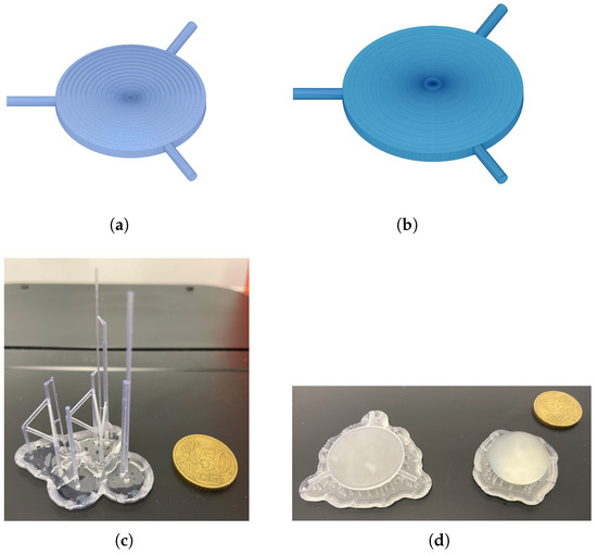
Figure 1.
(a) CAD design of Fresnel lens, (b) CAD design of plano-convex lens, (c) additively manufactured unprocessed WG prototypes, (d) additively manufactured unprocessed lens prototypes.
We then used the same Formlabs Clear resin V4 as the agent for dip-coating. This has the advantage that the same material is used for AM and dip-coating, resulting in perfect refractive index matching and matching thermal parameters. At room temperature, the photosensitive resin features a viscosity similar to honey. To lower the viscosity and achieve thinner and more homogeneous coating films, the resin was heated using a magnetic stirrer with a heating plate to temperatures of up to 70 °C under a fume hood to remove toxic gases. The viscosity was then similar to that of water. We verified that the temperature of the heated photosensitive resin remained constant throughout the dip-coating process. We then immersed the 3D-printed optical components in the liquefied resin for 10 s. This duration was estimated empirically and based on successive experimentation to achieve a uniform surface finish. We analyzed the dip-coated samples after each coating to check the irregularities. We observed that a dip duration of less than 10 s may lead to the formation of satellite droplets on the coated surface. Subsequently, the dip-coated optical component prototypes were hardened using Formlabs Form Cure for 20 min without heating, using suitable prototype holders so that the optically active surfaces of the coated prototypes remained untouched. In the case of dip-coating Fresnel lenses, only the flat surface of the lens was dip-coated initially and the surface with the annular rings remained intact. In Step 2, we immersed the surface with annular rings only for a fraction of a second, and then the lens was gently shaken until the excess satellite droplets from the surface came off. This method ensured that the annular rings of the Fresnel lens were not coated in such a way that the lens properties changed dramatically. Figure 2 depicts the steps involved in the dip-coating process. As the dip-coated resin layer is cured using UV light without mechanical interaction, the dip-coated layer provides a perfect surface finish and is expected to remain stable over the long term.
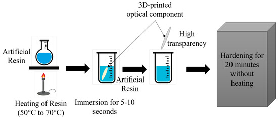
Figure 2.
Dip-coating process.
An alternative and simple approach to the heating of Formlabs Clear resin V4 is to place the beaker containing the resin solvent in hot water with an initial temperature of up to 70 °C. Convection heating allows the resin to warm uniformly to a temperature of 60 °C, yielding a viscosity similar to maple syrup. We investigated this approach for further optimization with increased water temperatures of up to 90 °C, and a viscosity similar to that of water was achieved for a short period of five minutes.
3. Results and Discussion
After manufacturing the WGs and lens prototypes and subsequent photosensitive resin-based dip-coating, we measured their surface roughness. First, we visually inspected the manufactured components using a Keyence VHX7000 microscope primarily at the corners and edges of the waveguides and at the center of the lenses where the light guiding takes place in order to check whether the structures were intact and optically smooth. In the first step, we used the same Keyence VHX7000 microscope with an X500-X5000 objective to measure the surface roughness of the uncoated samples. This microscope has a measurement resolution of 100 nm. The roughness computation was carried out using the depth-of-field recording method and subsequent 3D reconstruction of the surface, yielding the surface roughness as an arithmetic average (), that is, the deviation of surface roughness from the mean height. It turned out that the resolution of the microscope was insufficient to resolve the actual roughness. We used the DEKTAK 6M surface profiler from the Bruker Corporation. This profiler is well suited for surface coating measurements as it features a height resolution on the order of 1 nm. We opted for a profilometer instead of an atomic force microscope (AFM), as it is much faster, and previous research has shown that accuracy is comparable for surface roughnesses above a few nm [35].
Surface roughness and waviness were analyzed using the factory-installed evaluation software of the DEKTAK 6M without any filtering. The scan length was varied between 50 µm and 1 mm in order to probe local roughness and global waviness. We chose the smallest height resolution tolerated by the waviness of the sample (6.5 µm or 65.5 µm height measurement range). The authors also measured unprocessed 3D-printed samples using the DEKTAK 6M device and found that the surface roughness ranged from 3 µm to 8 µm, which nearly matched the measurements carried out using the Keyence VHX7000 microscope. The surface roughness of the dip-coated prototypes was within the range of the system’s resolution, i.e., ~5 nm. We observed a superimposed curvature on the order of 10/m and some defects with wavy features on the order of 0.25–0.5 μm on the surface. These features were small compared to the coating thickness of 20 μm. These minor defects may be a reaction to the hardening process after dip-coating, which can be avoided through process optimization. Table 1 compares the surface roughnesses achieved after different post-processing techniques, e.g., polishing and lacquering.

Table 1.
Comparison of surface roughnesses after applying various post-processing methods.
We also measured the approximate thickness of the dip-coating layer. For this, we used rectangular WG structures with a cross-section of 1 mm × 1 mm and 500 μm × 500 μm, followed by dip-coating. The cross-section of the dip-coated WGs was observed to be similar to the previous measurements using the Keyence VHX-7000 microscope equipped with the X500-X5000 objective (Appendix A). After repeating the observation and measurements at the corners of multiple WG prototypes axially and laterally, we validated the results to approximate the thickness of the dip-coating layer as 21 ± 3 μm.
In order to ascertain that the dip-coating process does not cause additional losses, we verified the optical attenuation using the cut-back technique based on [36] and a 1550 nm laser beam Thorlabs MCLS1. The laser beam diameter of 1 mm was adjusted using a commercial lens with a focal length of 4 cm. For reference, the beam initially propagated through free space. After that, the laser beam was again passed through both the rectangular and circular WGs mounted on suitable opto-mechanical holders. An iris was used to avoid the direct line-of-sight coupling of the laser beam into the power meter. On the receiver side, we used an optical power meter (Thorlabs PM320E with a Thorlabs S122C sensor head). Figure 3 shows the attenuation of the WGs obtained for different rectangular and circular WGs before and after dip-coating, along with the SD. Compared to our previous results in Section 1, the waveguiding losses ranged from 1 to 1.5 dB per cm of the WG. Before and after dip-coating, the losses were reduced by more than 4 dB in all cases, in agreement with a previous measurement in which we found an improvement of 5 dB [3]. We deduced that the remaining losses predominantly originated from material absorption and coupling losses. Moreover, rectangular WGs seemed to feature slightly lower losses than circular WGs. The distribution of dip-coated resin material over rectangular WGs, compared to circular WGs, can be attributed to the dipping angle and the position of the WGs inside the resin material.
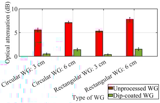
Figure 3.
Optical attenuation for unprocessed and dip-coated WGs.
We also dip-coated plano-convex lenses and Fresnel lenses with Formlabs Clear Resin V4. Figure 4 shows the difference between the unprocessed lens prototypes and the dip-coated lens prototypes. The significant improvement in transparency is apparent. The dip-coated lens does not show any physical colors as they would appear due to Fabry-Pérot interference if the refractive index of the coating layer was not identical to that of the lens.
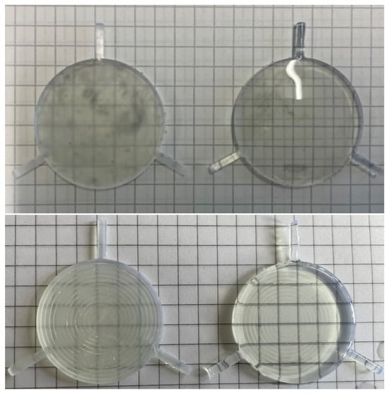
Figure 4.
Optical quality and transparency achieved after dip-coating of plano-convex (top) and Fresnel lens (bottom).
Last but not least, we characterized the focal length of the manufactured and dip-coated lenses. As previously implemented for characterization, we used a wavelength of 1550 nm derived from the Thorlabs MCLS1 laser source. We measured the power on the optical axis by varying the distance between the plano-convex lens and sensor head in steps of 1 mm, using a Newport MM4006 automated motion controller equipped with Newport CMA25CCCL motors connected to the XYZ-stage. The optical power was measured using a Thorlabs PM320E with a Thorlabs S122C sensor head. Subsequently, the optical attenuation was calculated for both the unprocessed and dip-coated plano-convex lens prototypes. The focal length of the dip-coated plano-convex lens was 3.1 ± 0.2 cm. We repeated the experiment for the Fresnel lens, obtaining a focal length of 2.2 ± 0.1 cm, very close to the design focal length of 2 cm. We analyzed multiple unprocessed and dip-coated lens prototypes to approximate the typical error characteristics. The focal lengths of the dip-coated lens prototypes were within the range of the manufacturing tolerances. This also confirms that the dip-coating process has minimal effect on the overall functioning of the lens prototypes.
Based on the results of dip-coating using Formlabs Clear Resin V4, the authors experimented with the dip-coating process on some thermoplastics with nearly equal refractive indices, e.g., cyclic olefin copolymer (COC/TOPAS) and Acrylonitrile Butadiene Styrene (ABS), achieving a consistent coating layer thickness of approximately 25 μm. Moreover, the authors investigated a further photosensitive resin (Phrozen Aqua Clear) for the dip-coating of structures printed with Formlabs Clear Resin V4 with almost the same refractive index (1.49). The future scope of this research involves testing the same process using a wide variety of materials, e.g., Ormocore, SU-8.
4. Conclusions
This work validates the effectiveness of post-processing of additively manufactured optical components with a dip-coating process using the same resin previously used for AM. The surface roughness caused by the printing process in the range of 10 ± 3 μm was reduced to the 5 nm level, enabling shiny, optically smooth surfaces. The inexpensive dip-coating process only requires heating of the resin (Formlabs Clear Resin V4) to 70 °C, where the viscosity becomes similar to that of water, resulting in a coating thickness of 21 ± 3 μm. The resin distributes uniformly over the surface of 3D-printed objects with some minor curvature toward the edges. As the same resin is used for manufacturing and coating, there are no Fabry-Pérot effects visible, proving close to perfect refractive index matching. We also confirmed that the difference between the design focal length and the focal length of the dip-coated component was only 3.3%, which is on the order of the measurement and 3D-printing accuracy. When compared to previous research and state-of-the-art technologies, the results and observations allow us to deduce that the dip-coating process is a feasible and economical approach for the post-processing of 3D-printed optical components, providing a promising surface roughness in the nanometer range with optical quality. Future work will aim to optimize the process and investigate implementations for scaling up the dip-coating process toward industrial applications. Further investigations will focus on dip-coating processes for a wider range of thermoplastics and UV-curable photosensitive resins, as well as optical structures with feature sizes in the micron range, which are achievable with advanced printing techniques, e.g., ultra-precise dispensing. This will require thinner coating layers, i.e., higher deposition temperatures of the resin to achieve thinner films. It may also require alternative coating processes like vapor deposition (as used for hexamethyldisiliazane (HMDS)), which could enable nanometric coating layer thicknesses.
Author Contributions
Conceptualization, A.S.; Methodology, A.S.; Validation, A.S.; Formal analysis, A.S. and S.P.; Investigation, A.S.; Writing—original draft, A.S.; Writing—review and editing, S.P. and O.S.; Supervision, S.P. and O.S.; Project administration, A.S., S.P. and O.S.; Funding acquisition, S.P. and O.S. All authors have read and agreed to the published version of the manuscript.
Funding
This research was funded by Deutsche Forschungsgemeinschaft (German Research Foundation) under grant number 502254396.
Institutional Review Board Statement
Not applicable.
Informed Consent Statement
Not applicable.
Data Availability Statement
The raw data supporting the conclusions of this article will be made available by the authors upon reasonable request.
Acknowledgments
The authors would like to thank Tobias Christophliemke for his input to this new approach and for making all the test environments available in the laboratory. We also acknowledge the Open Access Publishing Fund of the Technical University of Darmstadt for the article processing charges.
Conflicts of Interest
The authors declare no conflicts of interest.
Appendix A. Supporting Data
This section gives an overview of measurement results evaluated for a 3D-printed cube sample with a volume of 1 cm3 carried out using the Keyence VHX7000 and DEKTAK 6M microscopes.
Appendix A.1. Measurements Using the Keyence VHX7000
The authors would like to note that the surface roughness of the cube samples depicted in Figure A1 and Figure A2 provides an overview of the average surface roughness over the measurement area ()—in these particular cases, within the red circle of area 2.85 mm2.
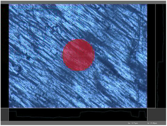
Figure A1.
Surface roughness of unpolished cube sample over a 2.85 mm2 area, measured using a Keyence VHX7000 microscope.
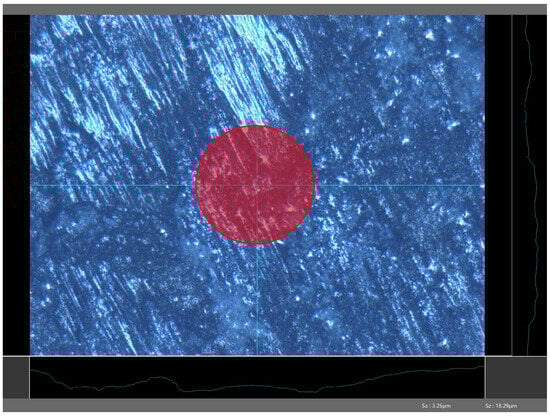
Figure A2.
Surface roughness of polished cube sample over a 2.85 mm2 area, measured using a Keyence VHX7000 microscope.
Appendix A.2. Measurements Using the DEKTAK 6M
Figure A3 shows an evaluation of the surface roughness measurement results of the cube sample with a 50 μm scan (left) and a 1 mm (right) scan using a DEKTAK 6M microscope. Among these, the 1 mm scan (right) depicts the wavy features discussed earlier. This wavy feature, rather than curvature, is measured at the center of the cube sample over an area of 2 mm2.
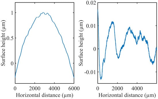
Figure A3.
Evaluation of surface roughness measurements using a DEKTAK 6M device, depicting a 50 μm scan (left) and a 1 mm scan (right).
References
- Berglund, G.; Wisniowiecki, A.; Gawedzinski, J.; Applegate, B.; Tkaczyk, T. Additive manufacturing for the development of optical/photonic systems and components. Optica 2022, 9, 623–638. [Google Scholar] [CrossRef]
- Heinrich, A. 3D Printing of Optical Components; Springer Series in Optical Sciences 2020; Springer: Berlin/Heidelberg, Germany, 2020; ISBN 978-3-030-58959-2. [Google Scholar] [CrossRef]
- Shrotri, A.; Beyer, M.; Stübbe, O. Manufacturing and analyzing of cost-efficient fresnel lenses using stereolithography. In Proceedings of the SPIE 11349 2020, 3D Printed Optics and Additive Photonic Manufacturing II, 113490N, Online, 6–10 April 2020. [Google Scholar] [CrossRef]
- Elkaseer, A.; Chen, K.; Janhsen, J.; Refle, O.; Hagenmeyer, V.; Scholz, S. Material jetting for advanced applications: A state-of-the-art review, gaps and future directions. Addit. Manuf. 2022, 60, 103270. [Google Scholar] [CrossRef]
- Beyer, M.; Shrotri, A.; Stübbe, O. Evaluation of stereolithography processes for the production of lens prototypes. In Proceedings of the Production Engineering and Management, Trieste, Italy, 3–4 October 2019; pp. 227–239. [Google Scholar]
- Zigon, J.; Kariz, M.; Pavlic, M. Surface Finishing of 3D-Printed Polymers with Selected Coatings. Polymers 2020, 12, 2797. [Google Scholar] [CrossRef] [PubMed]
- Shrotri, A.; Mukherjee, A.K.; Lohöfener, S.; Springer, A.; Stübbe, O.; Preu, S. Additive manufacturing and characterization of hollow core metal and topas waveguides for Terahertz sensor systems. In Proceedings of the 48th International Conference on Infrared, Millimeter, and Terahertz Waves (IRMMW-THz), Montreal, QC, Canada, 17–22 September 2023; pp. 1–2. [Google Scholar] [CrossRef]
- Available online: https://de.statista.com/statistik/daten/studie/289933/umfrage/umsatz-der-deutschen-photonik-industrie/ (accessed on 29 November 2024).
- Available online: https://de.statista.com/statistik/daten/studie/1078952/umfrage/umsatz-mit-3d-druck-weltweit/ (accessed on 29 November 2024).
- Shrotri, A.; Wittenbröker, C.; Preu, S.; Stübbe, O. Design and simulation of a nozzle-mask for optical fiber 3D-printing. In Proceedings of the SPIE 12995 2024, 3D Printed Optics and Additive Photonic Manufacturing IV, 129950A, Strasbourg, France, 7–12 April 2024. [Google Scholar] [CrossRef]
- Golhin, A.; Tonello, R.; Frisvad, J. Surface roughness of as-printed polymers: A comprehensive review. Int. J. Adv. Manuf. Technol. 2023, 127, 987–1043. [Google Scholar] [CrossRef]
- Hari, A.; Patadiya, J.; Kandasubramanian, B. Recent advancements in 3D printing methods of optical glass fabrication: A technical perspective. Hybrid Adv. 2024, 7, 100289. [Google Scholar] [CrossRef]
- Vaidya, N.; Solgaard, O. 3D printed optics with nanometer scale surface roughness. Microsyst. Nanoeng. 2018, 4, 18. [Google Scholar] [CrossRef] [PubMed]
- Trost, M. Light Scattering and Roughness Properties of Optical Components for 13.5 nm. Ph.D. Dissertation, Friedrich-Schiller-Universität Jena, Jena, Germany, 2015. Available online: https://www.db-thueringen.de/receive/dbt_mods_00027041 (accessed on 29 November 2024).
- Shrotri, A.; Mukherjee, A.K.; Stübbe, O.; Preu, S. THz-Characterization of Additively Manufactured Spiral Shaped Waveguides. In Proceedings of the IEEE 11th Asia-Pacific Conference on Antennas and Propagation (APCAP), Guangzhou, China, 19–22 November 2023; pp. 1–2. [Google Scholar] [CrossRef]
- Sarkar, A.; Sarmah, D.; Baruah, S.; Datta, P. An Optimized Dip Coating Approach for Metallic, Dielectric, and Semiconducting Nanomaterial-Based Optical Thin Film Fabrication. Coatings 2023, 13, 1391. [Google Scholar] [CrossRef]
- Rauh, F.; Bienek, O.; Sharp, I.; Stutzmann, M. Conversion of a 3D printer for versatile automation of dip coating processes. Rev. Sci. Instrum. 2023, 94, 083901. [Google Scholar] [CrossRef]
- Bhamra, T.; Tighe, B. Mechanical properties of contact lenses: The contribution of measurement techniques and clinical feedback to 50 years of materials development. Contact Lens Anterior Eye 2017, 40, 70–81. [Google Scholar] [CrossRef] [PubMed]
- Magazzù, A.; Marcuello, C. Investigation of Soft Matter Nanomechanics by Atomic Force Microscopy and Optical Tweezers: A Comprehensive Review. Nanomaterials 2023, 13, 963. [Google Scholar] [CrossRef] [PubMed]
- El Chawich, G.; El Hayek, J.; Rouessac, V.; Cot, D.; Rebière, B.; Habchi, R.; Garay, H.; Bechelany, M.; Zakhour, M.; Miele, P.; et al. Design and Manufacturing of Si-Based Non-Oxide Cellular Ceramic Structures through Indirect 3D Printing. Materials 2022, 15, 471. [Google Scholar] [CrossRef] [PubMed]
- Butt, M. Thin-Film Coating Methods: A Successful Marriage of High-Quality and Cost-Effectiveness—A Brief Exploration. Coatings 2022, 12, 1115. [Google Scholar] [CrossRef]
- Liang, L.; Chen, Y.; Zhang, B.; Zhang, X.; Liu, J.; Shen, C.; Cui, Y.; Guo, X. Optimization of dip-coating methods for the fabrication of coated microneedles for drug delivery. J. Drug Deliv. Sci. Technol. 2020, 55, 101464. [Google Scholar] [CrossRef]
- Berglund, G.; Tkaczyk, T. Enabling consumer-grade 3D-printed optical instruments—A case study on design and fabrication of a spectrometer system using low-cost 3D printing technologies. Opt. Continuum 2022, 1, 516–526. [Google Scholar] [CrossRef]
- Shan, Y.; Hua, J.; Mao, H. 3D Printing of Optical Lenses Assisted by Precision Spin Coating. Adv. Funct. Matter 2024, 34, 2407165. [Google Scholar] [CrossRef]
- Scherino, L.; Giaquinto, M.; Micco, A.; Aliberti, A.; Bobeico, E.; La Ferrara, V.; Ruvo, M.; Ricciardi, A.; Cusano, A. A Time-Efficient Dip Coating Technique for the Deposition of Microgels onto the Optical Fiber Tip. Fibers 2018, 6, 72. [Google Scholar] [CrossRef]
- Evertz, A.; Schrein, D.; Olsen, E.; Hoffmann, G.-A.; Overmeyer, L. Dip coating of thin polymer optical fibers. Opt. Fiber Technol. 2021, 66, 102638. [Google Scholar] [CrossRef]
- Di Palma, P.; Taddei, C.; Borriello, A.; De Luca, G.; Giordano, M.; Iadicicco, A.; Campopiano, S.; Sansone, L. Self-Assembled Colloidal Photonic Crystal on the Fiber Optic Tip as a Sensing Probe. IEEE Photonics J. 2017, 9, 1–11. [Google Scholar] [CrossRef]
- Bauckhage, Y.; Heinrich, A. Optimierung der Oberflächengüte additiv gefertigter transmittierender Optiken mittels Dip-Coating. In Proceedings of the DGaO-Proceedings 2018; ISSN: 1614-8436—urn:nbn:de:0287-2018-P053-6. Available online: http://www.dgao-proceedings.de (accessed on 5 January 2024).
- Trinh, T.; Smihi, M.; Koev, L.; Zielinski, R. Dip Coating Process for Optical Elements. US20040096577A1, 20 May 2004. [Google Scholar]
- Biteau, J.; Ford, C.; Glacet, A. Method of Dip-Coating a Lens. WO2011123132A1, 6 October 2011. [Google Scholar]
- Chekkaramkodi, D.; Jacob, L.; Shebeeb, M.; Umer, C.; Butt, H. Review of vat photopolymerization 3D printing of photonic devices. Addit. Manuf. 2024, 86, 104189. [Google Scholar] [CrossRef]
- Canning, J.; Clark, C.; Dayao, M.; de LaMela, D.; Logozzo, M.; Zhao, J. Anti-Reflection Coatings on 3D-Printed Components. Coatings 2011, 11, 1519. [Google Scholar] [CrossRef]
- Available online: https://formlabs.com/ (accessed on 1 March 2019).
- Wang, E.; Yang, F.; Shen, X.; Li, Z.; Yang, X.; Zhang, X.; Peng, W. Investigation and Optimization of the Impact of Printing Orientation on Mechanical Properties of Resin Sample in the Low-Force Stereolithography Additive Manufacturing. Materials 2022, 15, 6743. [Google Scholar] [CrossRef] [PubMed]
- Mei, L.; Guan, G. Profilometry and atomic force microscopy for surface characterization. Nano TransMed 2023, 2, e9130017. [Google Scholar] [CrossRef]
- Vlasov, Y.; McNab, S. Losses in single-mode silicon-on-insulator strip waveguides and bends. Opt. Express 2004, 12, 1622–1631. [Google Scholar] [CrossRef]
Disclaimer/Publisher’s Note: The statements, opinions and data contained in all publications are solely those of the individual author(s) and contributor(s) and not of MDPI and/or the editor(s). MDPI and/or the editor(s) disclaim responsibility for any injury to people or property resulting from any ideas, methods, instructions or products referred to in the content. |
© 2025 by the authors. Licensee MDPI, Basel, Switzerland. This article is an open access article distributed under the terms and conditions of the Creative Commons Attribution (CC BY) license (https://creativecommons.org/licenses/by/4.0/).