Article

Ultrahigh-Speed Deposition of Diamond-like Carbon on a Pipe Surface Using a Scanning Deposition Method via Local High-Density Plasma

1
Graduate School of Engineering, Gifu University, Gifu 501-1193, Japan
2
Graduate School of Natural Science and Technology, Gifu University, Gifu 501-1193, Japan
3
Department of Mechanical Engineering, Faculty of Engineering, Gifu University, Gifu 501-1193, Japan
4
Center for Applied Research of Plasma, Faculty of Engineering, Gifu University, Gifu 501-1193, Japan
*
Author to whom correspondence should be addressed.
Coatings 2025, 15(11), 1348; https://doi.org/10.3390/coatings15111348
Submission received: 15 October 2025 / Revised: 13 November 2025 / Accepted: 17 November 2025 / Published: 19 November 2025

Abstract

This study presents a highly effective method for depositing diamond-like carbon (DLC) films onto pipe substrates using a scanning deposition by plasma enhanced chemical vapor deposition. A microwave–sheath voltage combination plasma was employed to generate local high-density plasma along a rotating pipe. While conventional contact-mode deposition using a metal contactor suffers from arcing and surface damage due to unstable sliding contact during rotation, a non-contact deposition using a metal antenna was developed to overcome these limitations. Electromagnetic field simulations were conducted to evaluate microwave power absorption in various antenna geometries, showing that the flat-plate antenna demonstrated the most effective power coupling. Subsequent scanning deposition experiments to a rotating pipe using flat-plate antennas of different lengths revealed that the 100 mm configuration achieved the highest deposition volume rate (exceeding that of the contact-mode) while avoiding arcing. Optical emission observations during deposition confirmed the formation of high-density plasma surrounding the flat-plate antenna and Raman spectroscopy of the deposited film showed typical spectra of DLC films. The deposition rates of DLC-coated pipe showed no significant variation with respect to rotational angle, suggesting that rotation during deposition contributes to achieving uniform film thickness along the circumferential direction of the pipe.

1. Introduction

Diamond-like carbon (DLC) is one of the materials in demand as a protective coating due to its high hardness, superior wear resistance, and chemical inertness. In particular, its low frictional properties under both dry and lubricated conditions have led to the extensive commercialization across a wide range of mechanical components [1,2,3]. To fabricate DLC coatings, physical vapor deposition (PVD) or chemical vapor deposition (CVD) has conventionally been employed; however, these are often challenged by low deposition rates ranging from 0.1 to 2 μm/h, which significantly limit their throughput and hinder large-scale production [4].
To address these limitations, ultrahigh-speed (UHS) deposition techniques have been proposed; particularly, the microwave–sheath voltage combination plasma (MVP) method has garnered attention owing to its ability to generate dense plasma near the substrate [4]. In the MVP method, microwave power is transferred into DC plasma, allowing the formation of high-density plasma (electron density n e > 10 11 cm−3) near the substrate. This configuration is expected to significantly enhance the deposition rate by increasing the amount of precursor ions and radicals coming to the substrate. Experimental validation of UHS deposition using the MVP method has been successfully demonstrated by Kousaka et al., who reported Si-doped DLC (Si-DLC) films deposited at rates as high as 156 μm/h [4].
However, the deposition process using the MVP method faces challenges in achieving uniform plasma density, primarily due to microwave attenuation during propagation. For instance, Deng et al. reported a significant decline in the deposition rate with increasing distance from the microwave injection point when the microwave was introduced from one end of a long metal rod [5]. Similarly, our previous research evidenced non-uniformity in thickness along a 200 mm long pipe, where microwave power was applied from one end; the thickness gradually decreased along the axial direction [6].
To enable scalable and uniform deposition along the length of cylindrical substrates, a scanning deposition mechanism was developed that translates the region of localized high-density plasma axially. Our previous work demonstrated the feasibility of depositing Si-DLC films on the surface of pipes using microwave power introduced via a metal contactor [6]. However, when the pipe was translated while maintaining physical contact with the metal contactor, deposition was frequently disrupted by arcing. This electrical discharge was primarily attributed to unstable contact conditions between the moving pipe and the contactor. Friction-induced surface roughening and fluctuations in the contact pressure caused localized variations in electrical resistance, which in turn destabilized the electric field near the contact interface. This instability made it difficult to maintain consistent current flow, ultimately triggering arc discharges. Since arcing not only compromises coating quality but also poses a risk of equipment damage, it is critical to avoid such phenomena during deposition.
To overcome these challenges, we propose a new MVP configuration in which the metal contactor is spatially separated from the substrate surface by a small distance and instead functions as a microwave antenna to transfer power into the Direct Current (DC) plasma surrounding the antenna surface. This non-contact approach was specifically designed to suppress arcing while maintaining sufficient plasma density for uniform film deposition along the pipe. To optimize the geometry of the antenna for efficient microwave power transfer, electromagnetic wave simulations were conducted under various antenna geometries. Based on the simulation results, a promising antenna geometry was identified and subsequently applied in experimental trials to deposit Si-DLC films using the scanning method. The deposition volume rate achieved with this non-contact approach was then quantitatively compared to that obtained via the conventional contact-based method.

2. Experimental Method

2.1. Deposition

A schematic of the deposition system is shown in Figure 1. The substrate was a manganese steel (SAE 1541M-R) pipe with an outer diameter of 49 mm, placed vertically in the vacuum chamber. A motor for rotation was located on the atmospheric side at the top of the device, which was connected to the top end of the pipe. For scanning deposition, the pipe was rotated at 30 RPM. A quartz component was installed to seal the interface isolating the vacuum chamber from the atmosphere.
The deposition was conducted in two modes: contact and non-contact. For contact-mode depositions, a metal contactor was employed to generate MVP, which remained in direct contact with the pipe surface during the deposition process. The microwave generator operated at 2.45 GHz, and the microwaves were transmitted through a waveguide, passed via a coaxial cable, and delivered to the metal contactor through a quartz component. The microwaves propagated as surface waves primarily along the interface between the ion sheath and the plasma [4]. To generate DC plasma, both the metal contactor and the pipe were connected to the negative terminal of a DC power supply. A bias voltage of −500 V was applied to both components, with a bias frequency of 50 kHz and a pulse duration of 1 μs.
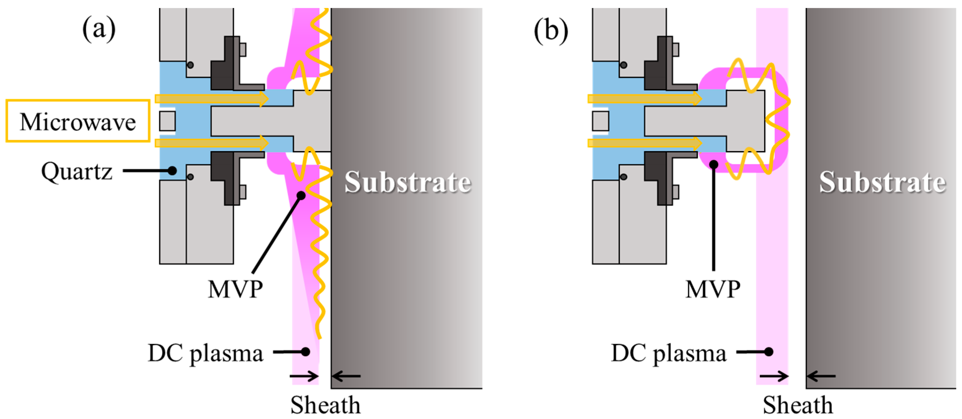
For non-contact mode deposition, the metal contactor was simply replaced by a metal antenna, positioned 4 mm above the pipe surface. In this configuration, the microwave propagated only around the metal antenna without directly interacting with the pipe surface. Figure 2 illustrates the plasma distribution near the pipe surface under the contact and non-contact modes. In the contact mode, the combination of microwave and DC plasma enables the formation of a high-density plasma over a broad area along the pipe surface because ion sheath layers along the pipe and the contactor form a continuous region (Figure 2a). In contrast, under the non-contact mode, the microwave energy is localized around the metal antenna because two sheath layers along the contactor and pipe are separated by high-density plasma surrounding the contactor, resulting in a narrower high-density plasma region compared to the contact mode (Figure 2b).
Si-DLC was selected as the top layer material due to its superior low-frictional properties, exhibiting coefficients of friction (COFs) in the range of 0.05–0.1, under dry-sliding conditions against steel, which are notably lower than those of a-C:H coatings [7,8,9,10]. Furthermore, Mori et al. reported a COF as low as 0.03 for Si-DLC sliding against nickel molybdenum steel (SAE4620) in lubricated conditions [9]. Si-DLC also exhibits outstanding tribological performance even under water lubrication, indicating its potential as an environmentally friendly coating.
Ar-plasma cleaning and intermediate-layer deposition were performed using DC voltage, whereas only the topmost layer simultaneously employed both microwave and DC voltage. The deposition time for the topmost layer was set to 240 s, and Ar, methane (CH4), and tetramethylsilane (TMS, Si (CH3)4) were used as precursor gases for the Si-DLC films. The deposition conditions are summarized in Table 1.
To determine the deposition rate, the film thickness was measured. Prior to deposition, several locations on the pipe surface were masked using marker ink. After deposition, the marker ink was removed, and the film thickness was determined using a surface profilometer (FORMTRACER Avant S3000, Mitsutoyo Corp., Kanagawa, Japan).
To analyze the structure of the resulting Si-DLC films, Raman spectroscopy (LabRAM HR800, HORIBA Co., Ltd., Kyoto, Japan) was carried out. A monochromatic laser with a wavelength of 515 nm was used as an excitation source. Raman signals were acquired with an exposure time of 20 s, two accumulations, and a spectral range of 800–2000 cm−1. Before the actual measurement, spectral calibration was conducted at 520 cm−1, which is the characteristic peak of a standard Si (100) wafer.

2.2. Electromagnetic Wave Simulation

For non-contact metal antennas, various antenna geometries and their microwave power absorption coupled to high-density plasma were investigated via RF module of COMSOL Multiphysics Ver. 6.3. Electromagnetic wave simulations were conducted for three different antenna geometries and the conventional metal contactor to evaluate the electromagnetic power loss density (W/m3), which reflects the spatial distribution of microwave power absorbed in plasma. The resulting power loss density distributions were compared to determine the most effective antenna geometry.
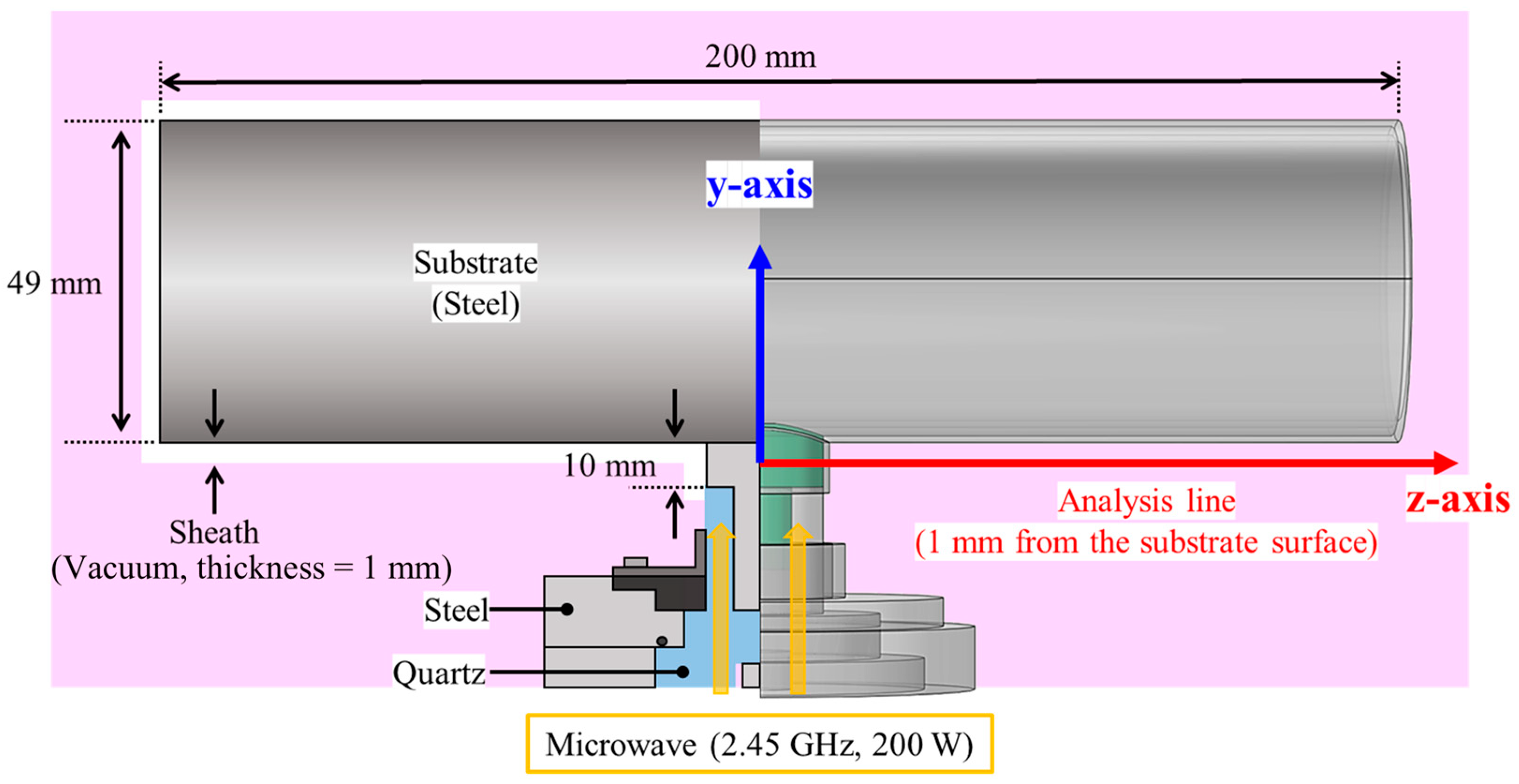
An example of the simulation model is shown in Figure 3, in which a metal contactor was used. In this simulation, the plasma was modeled as a homogeneous medium with constant electron density and fixed material properties. The thickness of the ion sheath formed on the biased metal antenna and pipe surface is calculated using the following equation:
d = 0.606 2 V 0 T e 3 / 4 λ D   [ mm ]
where V 0 is the sheath potential (500 V), T e is the electron temperature (2 eV) and λ D is the Debye length.
The Debye length. λ D is calculated as:
λ D = ε 0 T e n e e 2
where ε 0 is permittivity of vacuum, n e is the electron density in the plasma and e is the elementary charge. The calculated sheath thickness was 0.9526 mm for n e = 5 × 10 17   m 3 assumed in this work. Therefore, for the sake of simplicity in the simulation, the sheath thickness in all models was uniformly set to an approximate value of 1 mm.
The simulation parameters and material properties are listed in Table 2 and Table 3. The relative permittivity ε p and conductivity σ of the plasma are given by
ε p = 1 ω p 2 ω ω j ν e n
and
σ = e 2 n e m e ν e n ,
respectively, where m e is the electron mass, ω p is the electron plasma frequency, and ν e n is the electron-neutral collision frequency.
The value of ν e n , is given by
ν e n = K t n n
where the value of K t = 6 × 10 14 m3/s was set for Ar gas, and neutral gas density n n = P n k B · T n was calculated to be 1.55 × 10 22 m−3 for a gas pressure P n = 75   P a and temperature T n = 350   K .
The value of the electron plasma frequency ω p is defined as:
ω p = e 2 n e ε 0 m e .

3. Results and Discussion

3.1. Contact Deposition with Metal Contactor

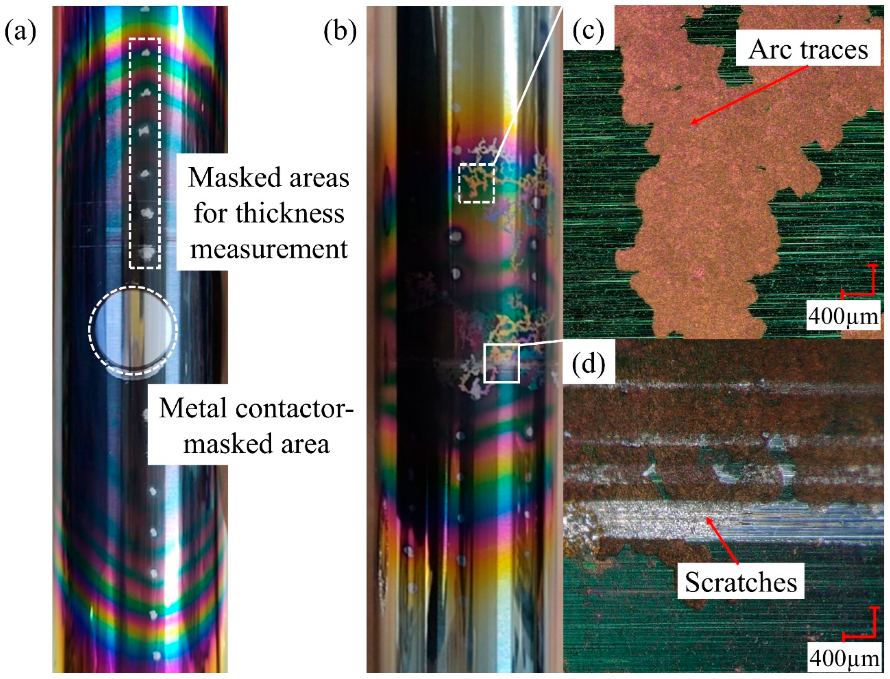
Figure 4 shows photographs of the pipe surfaces deposited via the contact mode. Figure 4a presents the surface of a pipe deposited without scanning; the highest deposition rate was calculated to be 37.5 µm/h. Figure 4b shows the surface of a pipe deposited by the rotational scanning method. Numerous arc traces and scratches were observed within the contact area, indicating inadequate deposition quality. The arcs were particularly pronounced during rotation, where friction between the moving pipe and the metal contactor contributed to unstable contact conditions. Surface roughening and fluctuations in contact pressure led to localized variations in electrical resistance, which destabilized the electric field at the interface; this instability hindered the maintenance of a consistent current flow, ultimately triggering arc discharges [6]. The scratch marks were similarly caused by mechanical friction. These observations highlight a critical limitation of contact-mode deposition and emphasize the necessity of separating the metal contactor from the pipe surface in scanning-based processes. However, one challenge in non-contact deposition is the reduced microwave propagation along the pipe surface, which can lead to lower deposition rates. Specifically, during non-contact deposition, microwave absorption occurred primarily along the antenna, resulting in diminished energy transfer to the pipe surface (Figure 2b). To overcome this limitation, the microwave antenna was redesigned based on the simulation results described in the following section.

3.2. Simulation of Microwave Propagation for Metal Antennas

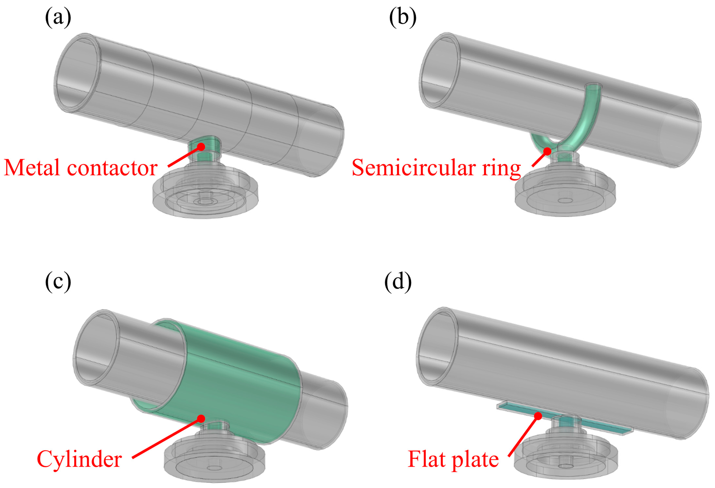
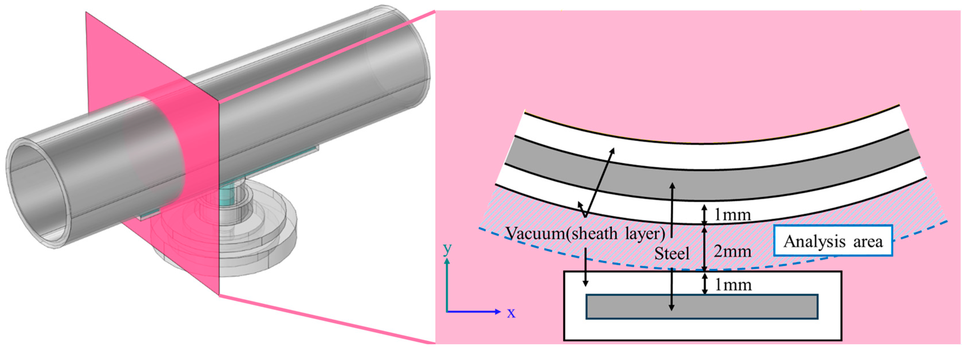
Figure 5 shows the simulation models of the conventional metal contactor (Model I) and three proposed antenna geometries (Model II-IV: Semicircular ring type, cylinder type, and flat-plate type). Model II consisted of a semicircular ring with a diameter of 10 mm. This design aims to reduce sharp edges and promote the circumferential propagation of microwaves along the pipe. Model III includes a cylindrical shell with an inside diameter of 61 mm, thickness of 1 mm, and length of 100 mm, positioned outside the pipe, which was expected to propagate microwaves along its inner surface and concentrate power deposition near the side surface of the pipe. Model IV features a flat-plate design with a thickness of 1 mm, a width of 10 mm and a length of 100 mm, intended to propagate microwaves across the planar surface and generate a high-density plasma region that extends in the axial direction between the antenna and the substrate. Model I corresponded to the conventional contact-type metal contactor and was included for comparison. A 4 mm gap was maintained between the pipe surface and the metal antenna in all models. As an example, Figure 6 shows a cross-sectional image of Model IV. Since both the pipe and the metal antenna surfaces are assumed to have 1 mm thick sheath layers, a 2 mm or higher-thick plasma region is formed between the two ion sheath layers.
To analyze the simulation results from the viewpoint of microwave absorption near the pipe, we defined an analysis line and area, as shown in Figure 3 and Figure 6. The analysis line was set to measure the distribution of the power loss density in the z-axis direction, aligned along the axial direction, and 1 mm away from the ion sheath layer on the bottom side of the cylinder. The analysis area was set to calculate the total electromagnetic power loss near pipe by integrating the power loss density within the area.
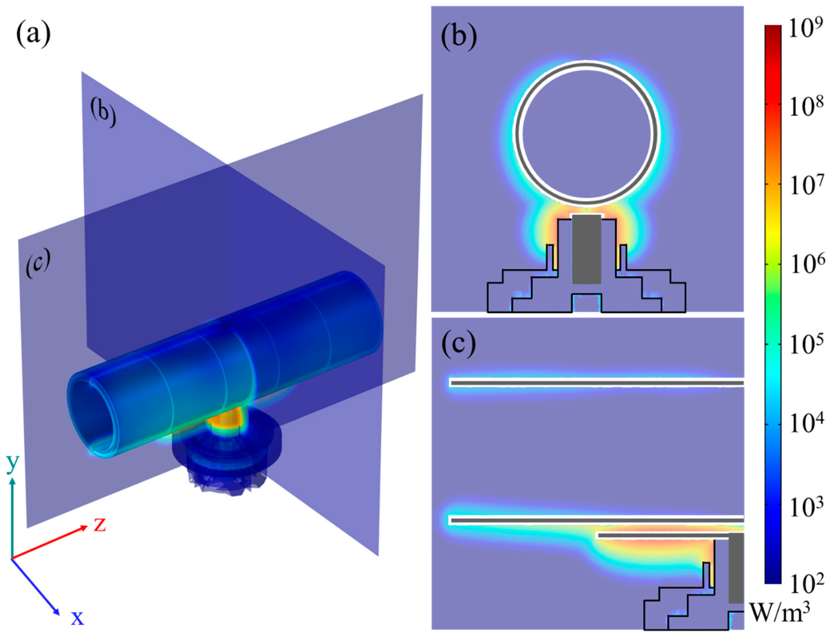
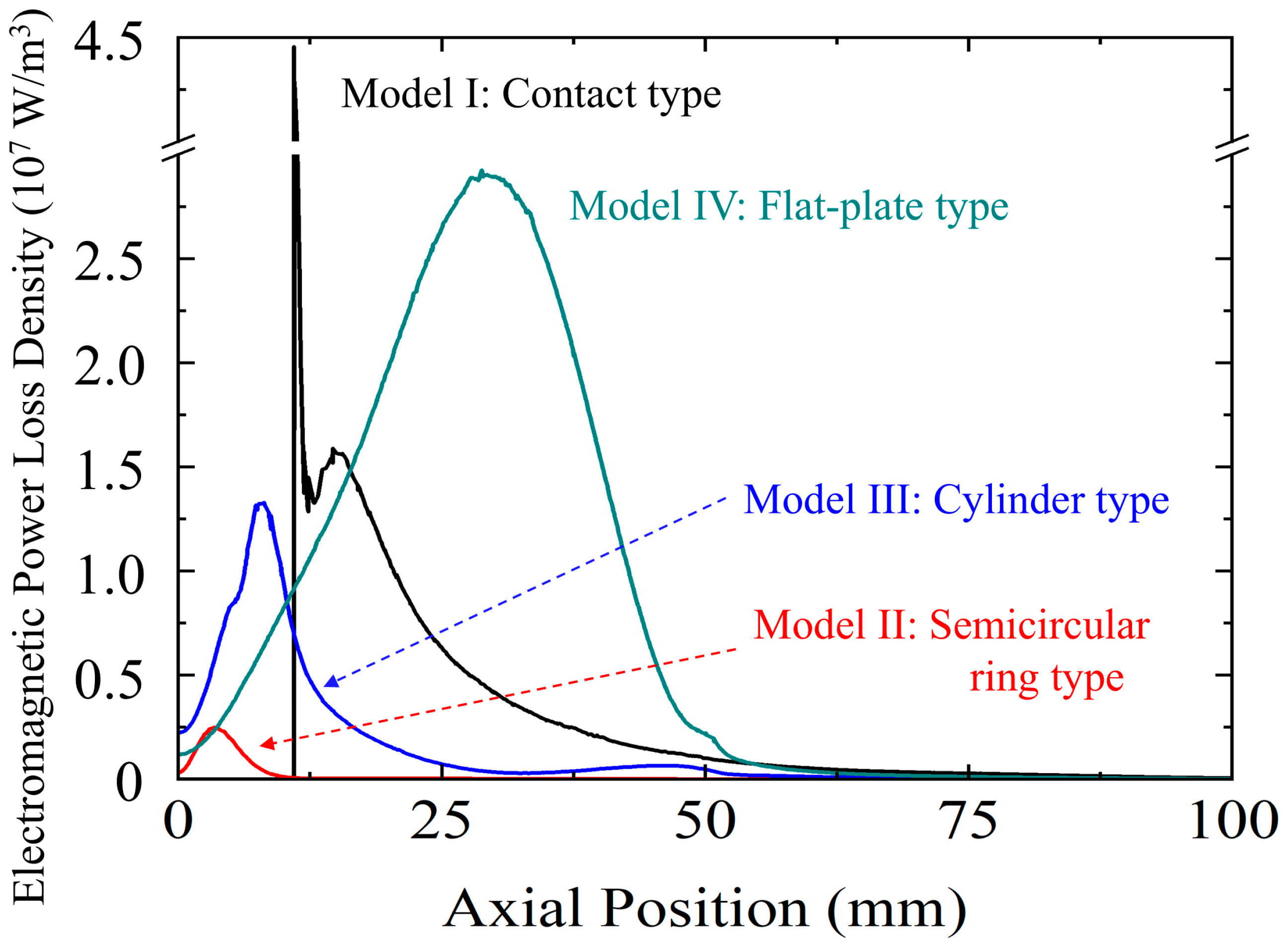
As representative simulation results, the spatial distributions of electromagnetic power loss density for the flat-plate antenna are illustrated from various viewing angles in Figure 7 (refer to Figure S1 for the results of the other antenna geometries). The axial distribution of power loss density along the analysis line for all models is presented in Figure 8. In all cases, the absorbed microwave power increased with distance from the antenna center, reached a maximum, and then gradually decreased. However, for Model I (metal contactor), no power absorption was observed up to an axial position of 10 mm, corresponding to the region where the contactor was in direct contact with the pipe surface. The curve for Model IV shows a distinct peak between the center and the edge of the flat plate, and the value of the curve is close to zero toward the end. This suggests that a standing wave is formed by the interference of a traveling wave propagating from the antenna center to the end of the flat plate and a traveling wave reflected at the end and heading toward the center. Among all models, Model IV exhibited the highest microwave power absorption along the analysis line.
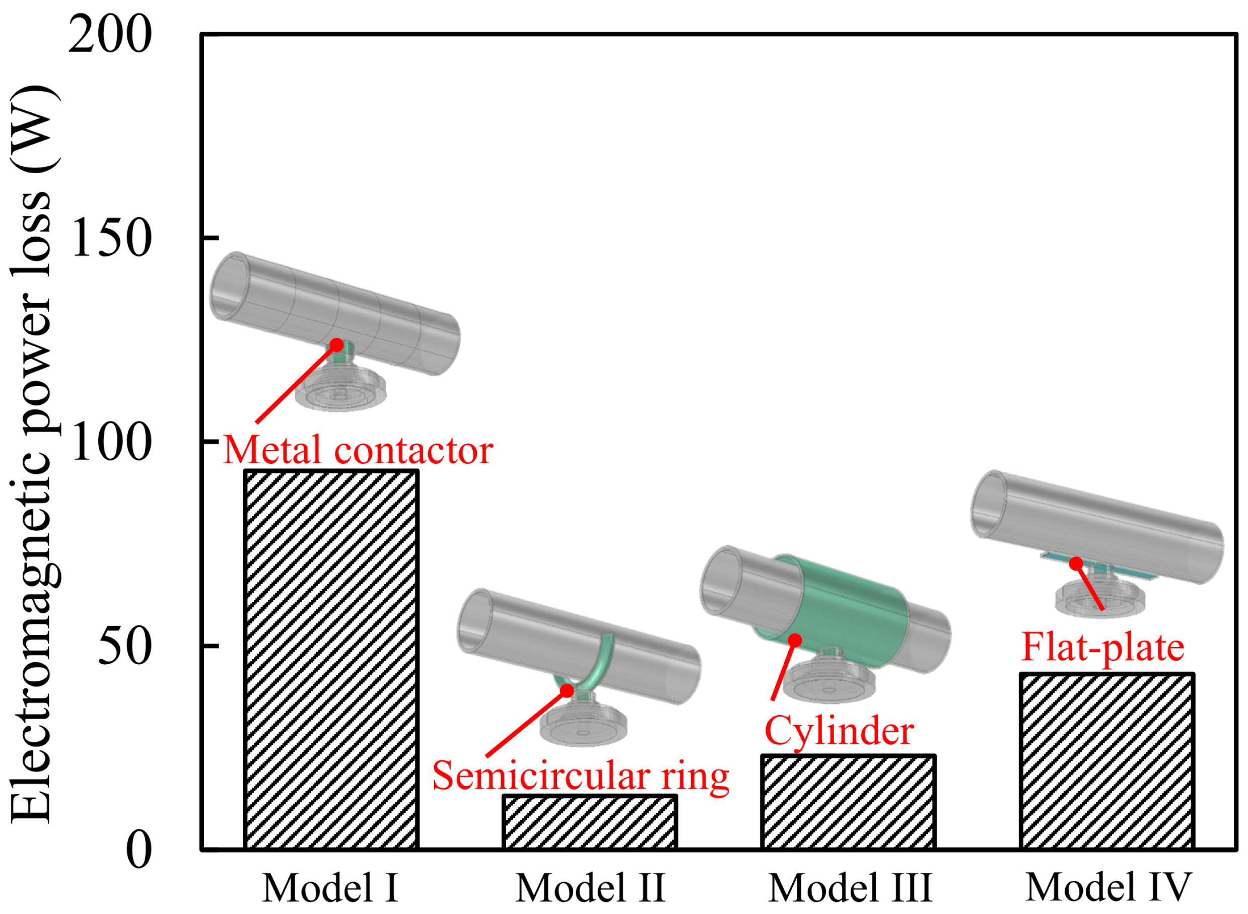
Figure 9 shows the total electromagnetic power absorbed in the defined analysis area. Figure S2 shows the distribution of the absorbed power across the segmented areas. Among the models, the contact-type (Model I) achieved the highest power absorption, with 92.85 W (46.4% of the 200 W input power) transferred into the plasma in the defined analysis area. In the case of non-contact models, the flat-plate antenna (Model IV) demonstrated the greatest efficiency within the analysis area, indicating 43.17 W (21.6%). Notably, three localized regions of intense absorption were observed in the flat-plate antenna (Model IV), suggesting a greater capability to sustain high-density plasma across a wider area compared to other antenna models.
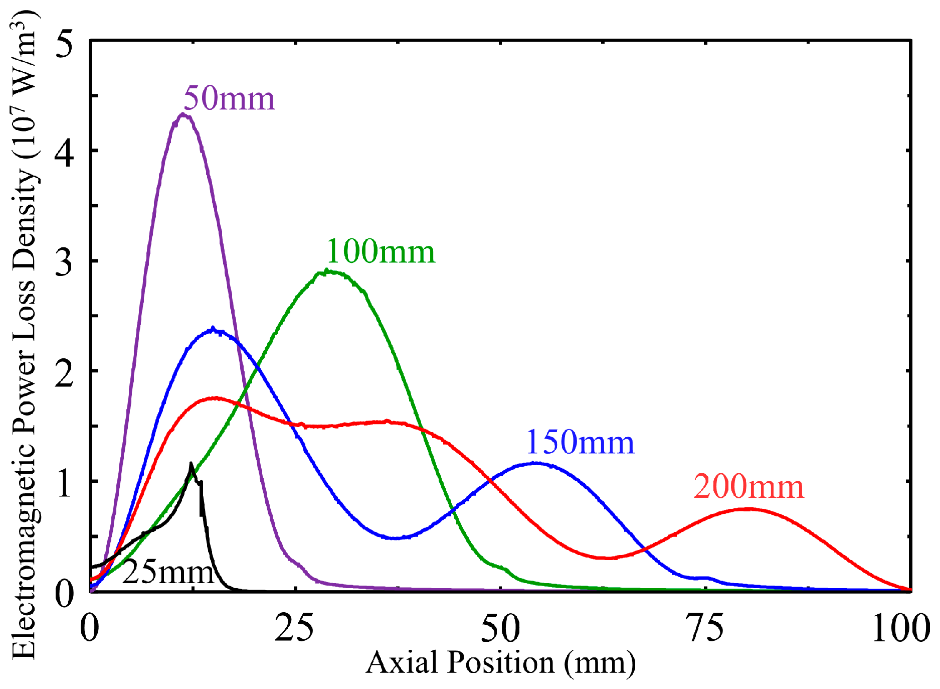
Based on these findings, we conducted further simulations of the flat-plate antenna (Model IV) to improve its performance by varying its length; five geometries were modeled, with antenna lengths of 25, 50, 100, 150, and 200 mm. Figure 10 shows the axial profiles of the electromagnetic power loss density along the analysis line. Among these geometries, 50 mm exhibited the highest peak value. The profiles for the 50 mm and 100 mm antennas show a single distinct peak located between the center and the edge of the flat plate, with the power loss density decreasing nearly to zero at the end. In contrast, the 150 mm and 200 mm models display two pronounced peaks along the axial direction, while also fading near the edge. These features are characteristic of standing wave formation, indicating that such waves are likely generated in the 50–200 mm range. On the other hand, the 25 mm model does not exhibit similar characteristics, suggesting that standing waves are not effectively formed at this length.

3.3. Non-Contact Deposition with Flat-Plate Antenna

Si-DLC films were deposited using five flat-plate antennas with different axial lengths (25, 50, 100, 150, and 200 mm). The deposition conditions were identical to those listed in Table 1. Figure 11 shows the results of scanning deposition of Si-DLC using the 100 mm long flat-plate antenna (photographs of deposition using antennas of other lengths are provided in Figure S3). Compared to conventional DC plasma (Figure 11a), plasma generated by the MVP method exhibited stronger optical emissions in the region between the flat plate and the pipe, indicating the formation of a high-density plasma (Figure 11b). See Video S1 for real-time footage of the deposition process using the 100 mm long flat-plate antenna. On the pipe surface directly facing the flat plate, interference colors were observed across a wide area, suggesting spatial variation in film thickness and an overall increase in deposition rate in this region (Figure 11c). This is attributed to the separation of ion sheaths between the antenna and the pipe during deposition, which confined microwave absorption to the geometry of the antenna.
Regarding the deposited film using 100 mm long flat-plate antenna (Figure 12), the surface roughness (Ra) exhibited no significant change compared to the pre-deposition surface, although the measured value increased slightly from 0.515 µm to 0.555 µm.
The adhesion between the Si-DLC film and the substrate was experimentally evaluated by a scratch test using a scratch tester (Scratch Tester CSR1000, RHESCA Corp., Tokyo, Japan) equipped with a diamond stylus (tip angle: 120°, tip radius: 200 µm). The test was performed on the Si-DLC deposited using a 100 mm long flat-plate antenna at the position corresponding to point B in Figure 12 with a film thickness of 0.8 µm. As shown in Figure S4, delamination of the Si-DLC film was observed at a critical load of 13.43 N, which was identified as the point where coating failure occurred during the progressive loading test. The corresponding scratch track, approximately 0.325 mm in width, shows partial cracking and localized deamination near this load. These results indicate that the Si-DLC film maintains sufficient adhesion to the substrate up to the critical load of 13.43 N. This value is within the typical range reported for well-adhered DLC-based films (10–20 N) [11,12,13], demonstrating that the deposited film possesses sufficient interfacial bonding strength between the Si-DLC and the substrate.
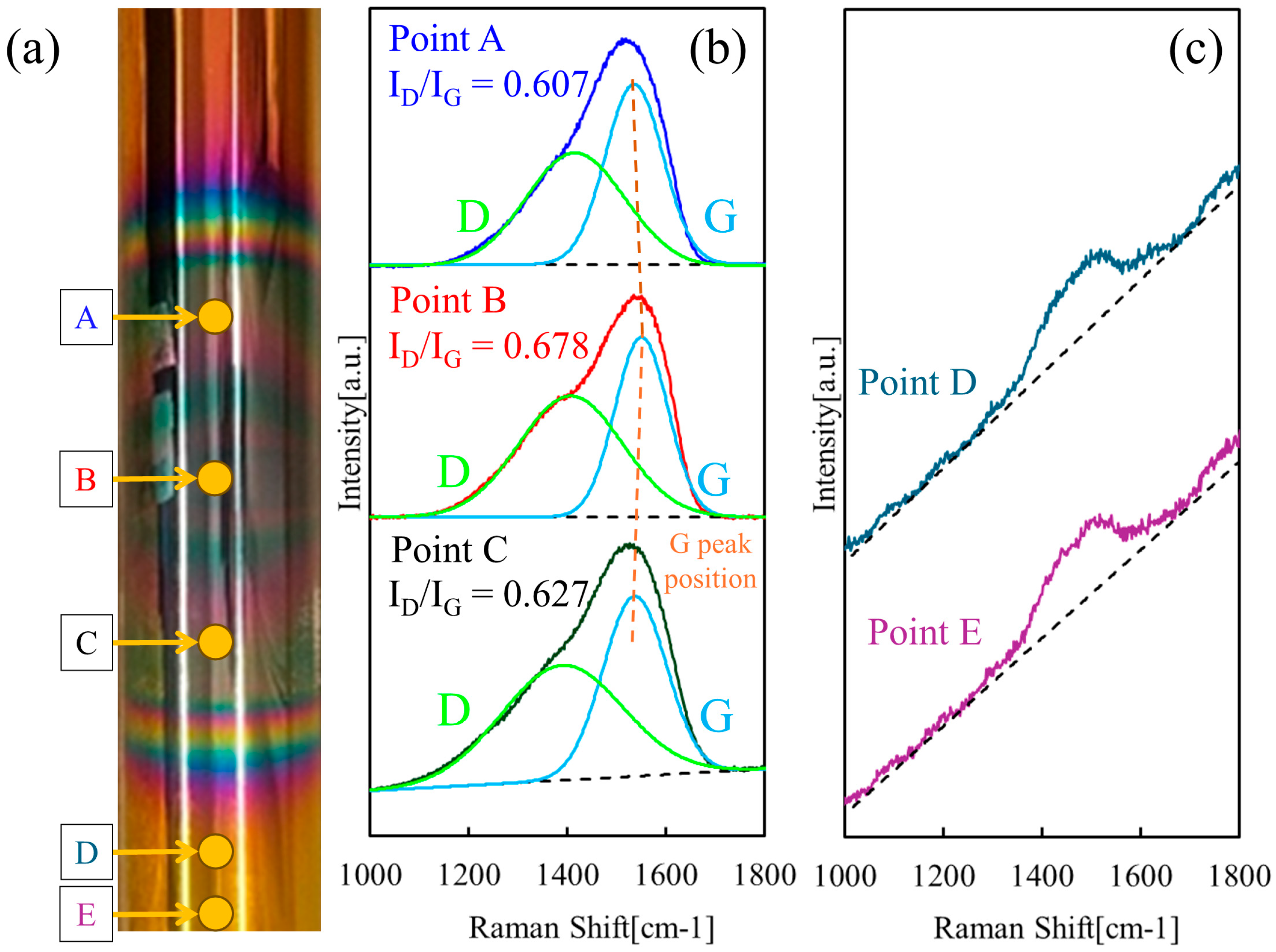
To evaluate the film quality, Raman spectroscopy was performed at five different locations, as shown in Figure 12a. Figure 12b,c present the Raman spectra corresponding to each measurement position. Since no change in interference colors was observed at points D and E, it is considered that these areas were not affected by microwaves, meaning that film deposition in these areas was carried out solely by DC plasma. The Raman spectra at points A–C show a typical DLC profile, characterized by two broad peaks—the D band and G band—acknowledged as the disordered sp2-bonded carbon network and graphitic vibrations, respectively. This indicates a hard amorphous carbon structure. In contrast, the spectra at points D and E show a higher baseline slope due to the presence of photoluminescence components. Choi et al. reported that, in DLC films, the slope of the Raman spectral baseline reveals a positive correlation with hydrogen content [14,15]. This suggests that points D and E contain a higher amount of hydrogen compared with points A–C, indicating that these regions possess a hydrogen-rich, polymer-like carbon (PLC) structure rather than a “diamond-like” structure. Thus, under the deposition conditions employed in this study, microwave irradiation appears to be essential for achieving DLC films.
Compared to the G peak position at point B, the peaks at points A and C are shifted toward lower wavenumbers. Likewise, the ID/IG ratios of points A and C are lower than that of point B. The ID/IG ratio, representing the relative intensity of the disorder-induced D band to the graphitic G band, is widely used as an indicator of the sp2 domain size and structural order in carbon-based materials. A lower ID/IG ratio suggests either reduced disorder or the dilution of carbon bonding networks due to silicon incorporation [16,17,18,19,20]. Choi et al. [20] have reported that, in typical Raman spectra of Si-DLC films, an increase in Si content leads to a decrease in ID/IG and a downward shift in the G peak. Based on these correlations, it is inferred that the Si-DLC film deposited near the center of the metal antenna (point B) contains less Si than those at the other positions (points A and C), where stronger Si-related features were observed.
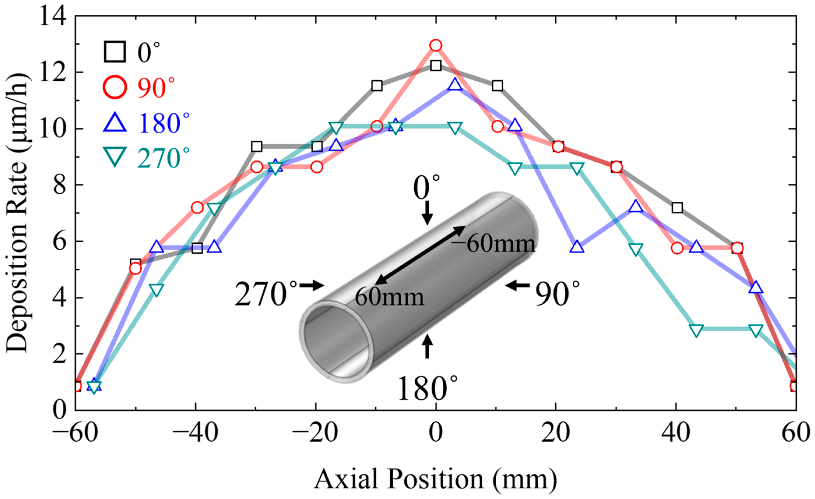
Figure 13 presents the deposition rates of the Si-DLC-coated pipe measured at four different rotational angles using a 100 mm long flat-plate antenna. The film thickness distribution used for calculating the deposition rate presented in Figure 13 is shown in Figure S5. The results showed no significant variation in deposition rate with respect to rotational angle, suggesting that rotation during deposition contributes to achieving uniform film thickness along the circumferential direction of the pipe. This finding implies that reciprocating the pipe along its axial direction during deposition could further promote uniformity of the film thickness in the axial direction as well.
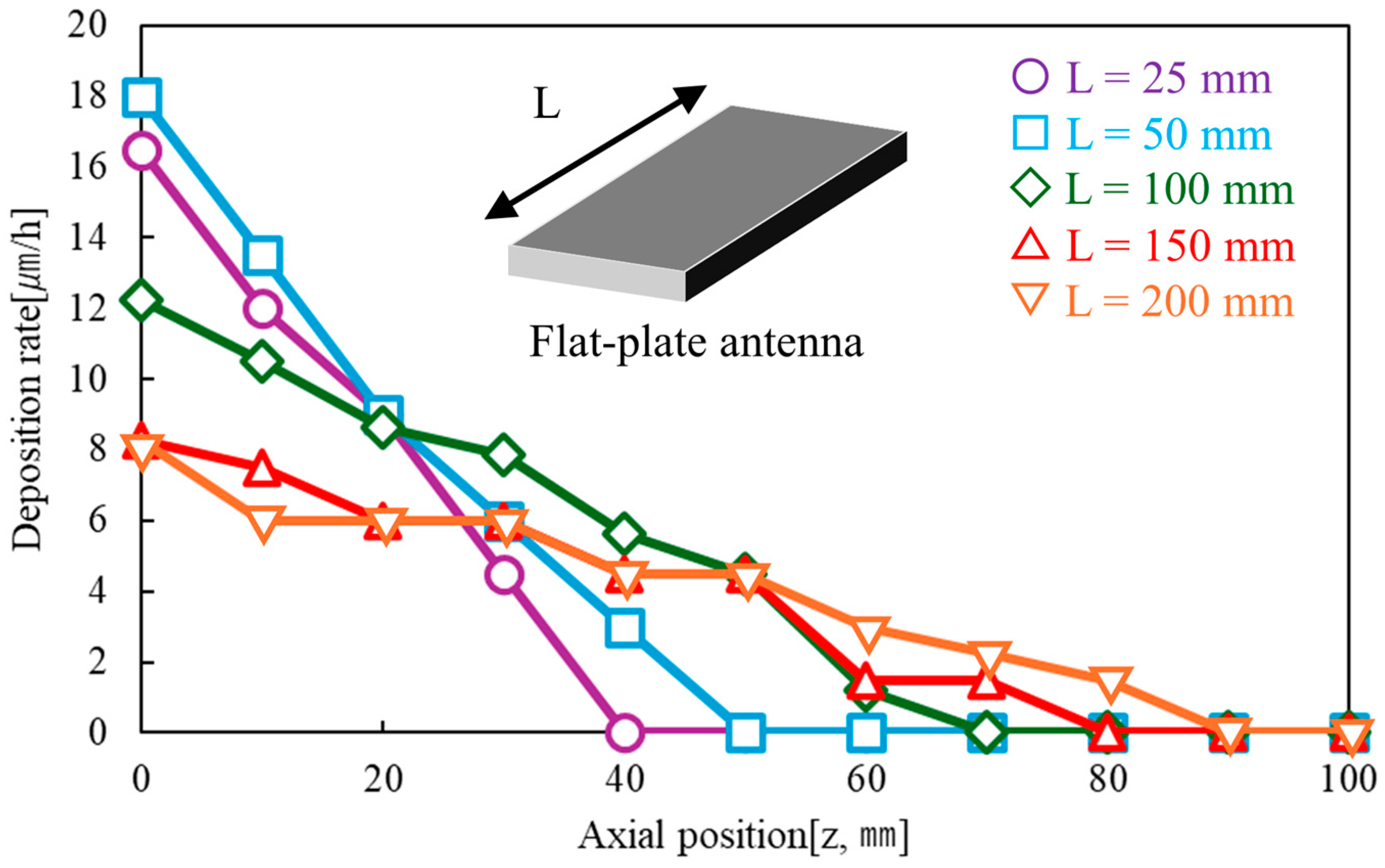
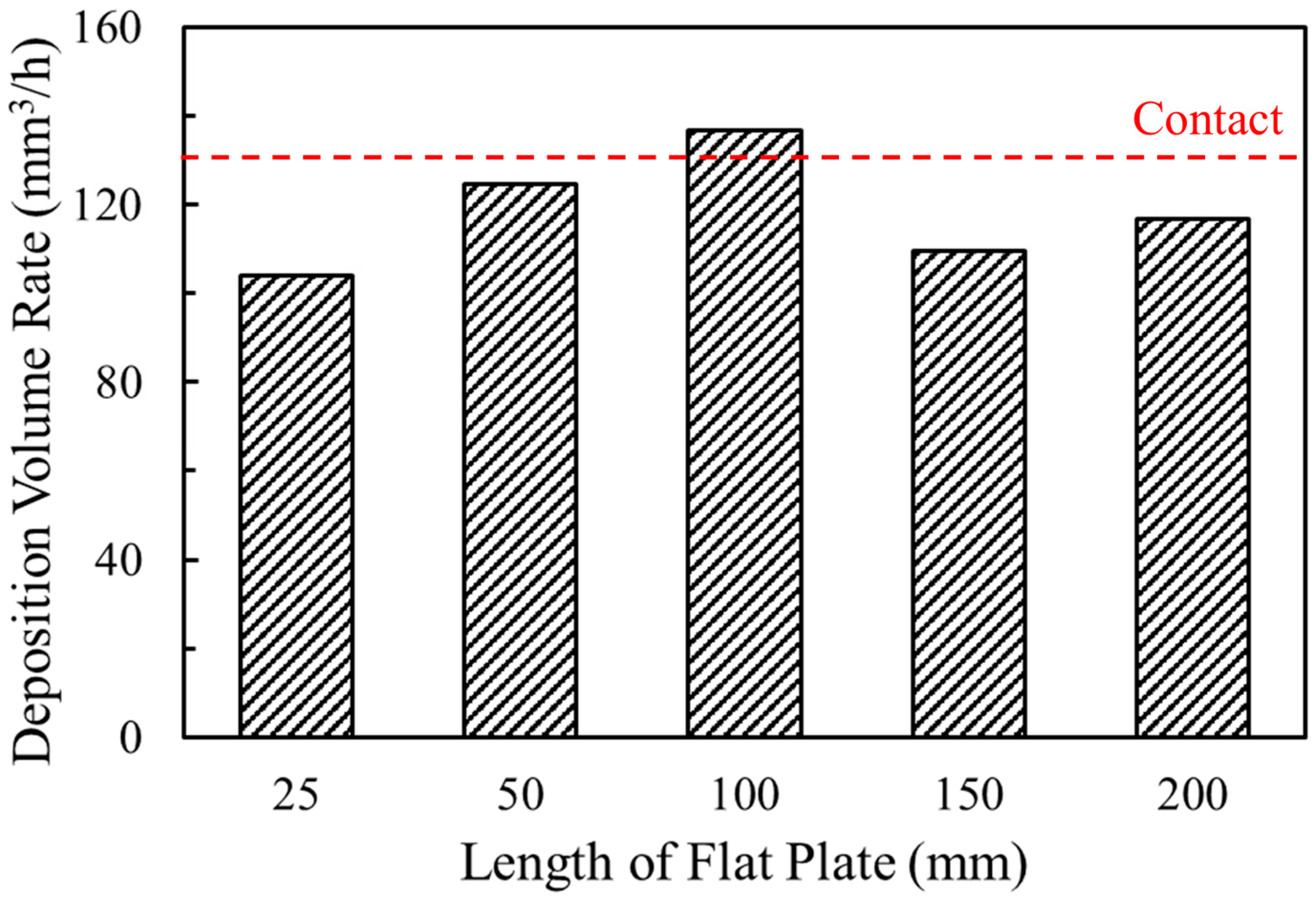
Figure 14 shows the axial distribution of deposition rates for various antenna lengths, and the corresponding deposition volume rates derived from these distributions are summarized in Figure 15. The film thickness distribution used for calculating the deposition rate, presented in Figure 14, is shown in Figure S6. In the thickness measurements, films thinner than 0.08 µm could not be accurately measured because the step height could not be distinguished from the surface roughness, and were therefore treated as having a thickness of zero. The deposition volume rates were calculated from the resulting film thickness distributions within a length of 200 mm of a pipe. The deposition volume rates [mm3/h] were calculated as:
2 π r 0 100 f x d x × 2
respectively, where r is the radius of the pipe, f ( x ) is the deposition rate distribution for each flat-plate length, as shown in Figure 14. In this paper, the piecewise quadrature method using data measured at 10 mm intervals was used in the integral calculation to obtain the deposition volume.
Among the prepared configurations, the antenna with a length of 100 mm yielded the highest deposition volume rate of 137 mm3/h. Importantly, the 100 mm long flat-plate antenna slightly outperformed the contact-mode configuration, which exhibited a deposition volume rate of 131 mm3/h.
Since the plasma in the gap between the pipe surface and the plate is considered to increase with increase in the total microwave power absorbed therein, the deposition volume rate is expected to be strongly correlated with the total microwave power (Pgap) absorbed in the gap. Note that we employed the line integral of curves presented in Figure 10 as an effective metric of Pgap. Figure 16 compares the line-integrated values (W/m2) of electromagnetic power loss density along the analysis line and the deposition volume rates, obtained for different lengths of the flat-plate antenna. In the cases of the 50, 100, 150, and 200 mm long flat-plate antennas, the change trend in the deposition volume rate with respect to the plate length fairly matches that in the line-integrated value of electromagnetic power loss density. This is thought to be because, as hypothesized above, the microwave absorption in the space between the pipe surface and flat plate has dominant influence on the deposition volume rate. However, from 50 to 25 mm, the decrease in deposition volume rate is much smaller than that in the line-integrated value of electromagnetic power loss density; in other words, in the case of shorter plate length, the amount of microwave absorption in the space between the pipe surface and the flat plate does not correlate well with the deposition volume rate.
Focusing on the fact that the power absorption near the pipe surface in the 25 mm long plate is significantly smaller than that in the other longer plates (Figure 10), the 200 W microwave input power in the simulation should be mostly absorbed by the plasma from the microwave inlet to the rear surface of the plate. (Note that the total microwave power absorbed in the simulation is 200 W under all calculation conditions.) Typically, the plasma generated by microwaves absorbed by regions other than the pipe surface also contributes to the deposition. Because this contribution is relatively large in the 25 mm long plate, it seems that there is less correlation between the power absorption near the pipe surface and the deposition volume rate, as shown in Figure 16. The better correlation between the integrated values and the deposition volume rates indicates that the simulation provides meaningful insights to a certain extent for a longer plate length than 50 mm.
The mismatch between simulated microwave absorption and experimental deposition volume rate is greatest for the following cases: although the 100 mm non-contact antenna achieved a higher deposition volume rate than the contact mode (Figure 15), its corresponding simulated power absorption within the analysis region was 43.17 W, substantially lower than the 92.85 W absorbed in the contact-mode model (Figure 9). This observation implies that in practical conditions, extremely localized and dense plasma (Figure S2) may lead to depletion of reactive species near the deposition zone [21]. The superior performance of the 100 mm non-contact antenna, which produces a moderately dense plasma distributed across a broader area, suggests that when increasing the plasma density on the side of the pipe for larger deposition volume rate, it may be better to distribute the microwave power over a wide area as much as possible rather than concentrating it locally.

4. Conclusions

The conclusions of this study are summarized as follows:
  • Contact deposition with scanning was initially attempted to achieve a localized UHS Si-DLC deposition using a circumferential scanning mechanism. However, this approach results in deposition defects due to arcs and surface scratches caused by physical contact. To address these problems, we developed a non-contact deposition employing a metal antenna.
  • To optimize the geometry of the metal antenna used in the non-contact deposition process, we analyzed microwave power absorption using COMSOL Multiphysics simulations. The results indicated that a flat-plate antenna exhibited the highest microwave absorption near the pipe surface, with an absorption power of 43.17 W under a 200 W input.
  • Antennas with lengths of 50, 100, 150, and 200 mm exhibited power loss density profiles characteristic of standing wave formation, with one or two distinct peaks depending on the specific length, whereas the 25 mm antenna did not display such features. These findings indicate that effective standing wave formation, and consequently improved microwave confinement, is achieved only when the antenna length exceeds a certain threshold.
  • Non-contact UHS Si-DLC deposition experiments were conducted using flat-plate antennas of different lengths. The deposition rate was evaluated within a range of −100 to 100 mm along the pipe. As a result, deposition volume rate of 137 mm3/h was achieved using 100 mm antenna, exceeding the 131 mm3/h rate obtained with the contact deposition.
  • Pipe rotation during non-contact deposition enables a uniform film thickness along the pipe circumference.

Supplementary Materials

The following supporting information can be downloaded at: https://www.mdpi.com/article/10.3390/coatings15111348/s1, Figure S1: Electromagnetic power loss density of (a–c) model I, (d–f) model II and (g–i) model III; Figure S2: (a) Image of analysis area in the COMSOL simulation (Blue area: measuring area, Green area: metal contactor) and (b) electromagnetic power loss in the measuring area (W) of 4 models; Figure S3: Photographs of flat-plate antenna and the process of UHS deposition process and the resulting pipes ((a,b) 25 mm, (c,d) 50 mm, (e,f) 150 mm and (g,h) 200 mm). Video S1: Movie of the process of UHS deposition process using 100 mm long flat-plate antenna.

Author Contributions

Conceptualization, H.K.; formal analysis, A.I., M.E. and T.N.; investigation, A.I., M.E. and T.N.; data curation, A.I., M.E. and T.N.; writing—original draft preparation, A.I.; writing—review and editing, A.I., H.K. and S.-M.B.; visualization, A.I. and S.-M.B.; supervision, H.K., S.-M.B. and T.H.; project administration, H.K.; funding acquisition, H.K. All authors have read and agreed to the published version of the manuscript.

Funding

This research was funded by JSPS KAKENHI, Grant Number JP23K22659.

Institutional Review Board Statement

Not applicable.

Informed Consent Statement

Not applicable.

Data Availability Statement

Data is contained within the article and Supplementary Materials.

Conflicts of Interest

The authors declare no conflicts of interest.

References

  1. Kano, M. Progress and Prospect of DLC Coating Applied Technologies to Automotive Engie Component. Jpn. J. Tribol. 2016, 61, 680–686. [Google Scholar] [CrossRef]
  2. Yamaguchi, Y.; Matsuoka, T.; Hirayama, T.; Asano, M.; Hanamoto, N. Tribological Property of DLC/DLC Sliding under Lubricated Condition with Oiliness Additive. J. Jpn. Soc. Mech. Eng. 2012, 2012, J111032. [Google Scholar] [CrossRef]
  3. Okubo, H.; Sasaki, S. Effects of lubricant additives on tribological properties of DLC films. Jpn. J. Tribol. 2018, 63, 11–19. [Google Scholar] [CrossRef]
  4. Kousaka, H.; Okamoto, T.; Umehara, N. Ultrahigh-Speed Coating of DLC at Over 100 μm/h by Using Microwave-Excited High-Density Near Plasma. IEEE Trans. Plasma Sci. 2013, 41, 1830–1836. [Google Scholar] [CrossRef]
  5. Deng, X.; Takaoka, Y.; Kousaka, H.; Umehara, N. Axial uniformity of diamond-like carbon film deposited on metal rod by using microwave–sheath voltage combination plasma. Surf. Coat. Technol. 2014, 238, 80–86. [Google Scholar] [CrossRef]
  6. Ito, A.; Nonomura, K.; Kousaka, H.; Furuki, T. Ultra-Fast Si-DLC Deposition using Non-Uniform High-Density Plasma Generated by Microwave Input from the Side of a Cylinder. J. Surf. Finish. Soc. Jpn. 2025, 76, 183–189. [Google Scholar] [CrossRef]
  7. Hioki, T.; Noda, S.; Isogai, A. Formation and Solid Lubricating Property of DLC(Diamond-Like Carbon). J. Surf. Sci. Soc. Jpn. 1991, 12, 227–232. [Google Scholar] [CrossRef]
  8. Mori, H.; Takahashi, N.; Nakanishi, K.; Tachikawa, H.; Ohmori, T. Low Friction Property of DLC-Si Films under Dry Sliding Condition. J. Surf. Finish. Soc. Jpn. 2008, 59, 401–407. [Google Scholar] [CrossRef]
  9. Mori, H.; Nakanishi, K.; Takahashi, N.; Kato, N.; Ohmori, T. Low Friction Mechanism of DLC-Si Films under Mineral Oil without Additive. Jpn. J. Tribol. 2009, 54, 40–47. [Google Scholar]
  10. Mori, H. Effect of Water in Lubricated Oil on Friction Property of DLC-Si Films. Jpn. J. Tribol. 2020, 65, 610–615. [Google Scholar] [CrossRef]
  11. Volosova, M.A.; Lyakhovetsky, M.; Mitrofanov, A.P.; Melnik, Y.A.; Okunkova, A.A.; Fedorov, S.V. Influence of Cr-Al-Si-N and DLC-Si Thin Coatings on Wear Resistance of Titanium Alloy Samples with Different Surface Conditions. Coatings 2023, 13, 1581. [Google Scholar] [CrossRef]
  12. Siddiqui, S.A.; Favaro, G.; Maros, M.B. Investigation of the damage mechanism of CrN and diamond-like carbon coatings on precipitation-hardened and duplex-treated X42Cr13/W tool steel by 3D scratch testing. J. Mater. Eng. Perform. 2022, 31, 7830–7842. [Google Scholar] [CrossRef]
  13. Zaidi, H.; Djamai, A.; Mathia, T. Characterisation of DLC coating adherence by scratch testing. Tribol. Int. 2006, 39, 124–128. [Google Scholar] [CrossRef]
  14. Choi, J.; Ishii, K.; Kato, T.; Kawaguchi, M. Evaluation and Prediction of Mechanical Properties of DLC Films by Raman Spectroscopy (Part 1). Jpn. J. Tribol. 2013, 58, 596–602. [Google Scholar] [CrossRef]
  15. Choi, J.; Ishii, K.; Kato, T.; Kawaguchi, M.; Lee, W. Structural and mechanical properties of DLC films prepared by bipolar PBII&D. Diam. Relat. 2011, 20, 845–848. [Google Scholar] [CrossRef]
  16. Robertson, J. Diamond-Like Amorphous Carbon. Mater. Sci. Eng. 2002, 37, 129–281. [Google Scholar] [CrossRef]
  17. Adamopoulos, G.; Robertson, J.; Morrison, N.A.; Godet, C. Hydrogen content estimation of hydrogenated amorphous carbon by visible Raman spectroscopy. J. Appl. Phys. 2004, 96, 6348–6352. [Google Scholar] [CrossRef]
  18. Ferrari, A.C.; Robertson, J. Interpretation of Raman Spectra of Disordered and Amorphous Carbon. Phys. Rev. B 2000, 61, 14095–14107. [Google Scholar] [CrossRef]
  19. Choi, J.; Hibi, T.; Furuno, A.; Kawaguchi, M.; Kato, T. Evaluation and Prediction of Mechanical Properties of DLC Films by Raman Spectroscopy (Part 2). Jpn. J. Tribol. 2017, 62, 228–235. [Google Scholar] [CrossRef]
  20. Choi, J.; Nakao, S.; Miyagawa, S.; Ikeyama, M.; Miyagawa, Y. The effects of Si incorporation on the thermal and tribological properties of DLC films deposited by PBII&D with bipolar pulses. Surf. Coat. Technol. 2007, 201, 8357–8361. [Google Scholar] [CrossRef]
  21. Wang, X.; Zhou, H.; Zhang, S.; Yan, M.; Lu, Y.; Hao, J.; Liu, W. The effect of acetylene flow rate on the uniform deposition of thick DLC coatings on the inner surface of pipes with different draw ratios. Vacuum 2022, 196, 110720. [Google Scholar] [CrossRef]
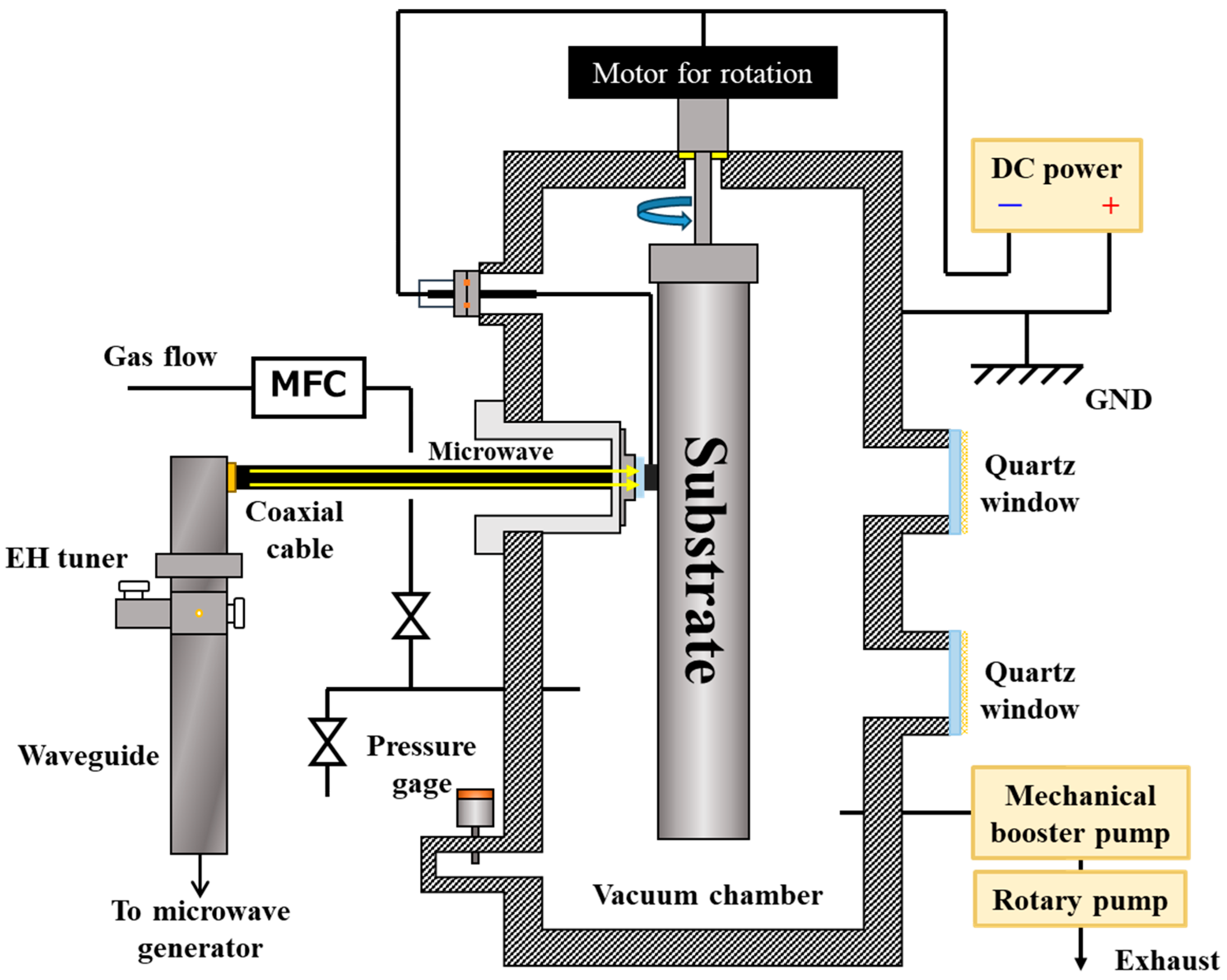
Figure 1. Schematic of the microwave–sheath voltage combination plasma (MVP) deposition system. In the figure, “MFC” stands for mass flow controller, and “EH tuner” stands for E-H plane tuner. The substrate, a manganese steel (SAE 1541M-R) pipe, was mounted vertically inside the vacuum chamber and electrically grounded (GND). A motor for scanning deposition was located on the atmospheric side at the top of the device and mechanically connected to the top end of the pipe. A quartz component was installed to seal the interface between the vacuum chamber and the atmosphere. Microwave power was transmitted through a waveguide, passed via a coaxial cable, and delivered to the metal contactor through the quartz component. To generate DC plasma, both the metal contactor and the pipe were connected to the negative terminal of a DC power supply.
Coatings 15 01348 g001
Figure 2. Illustration of the plasma distribution near the pipe surface. (a) The contact mode shows a high-density plasma over a broad area along the pipe surface because sheath layers of the pipe and the contactor form a continuous region. (b) The non-contact mode shows a narrower high-density plasma region because two sheath layers along the contactor and pipe are separated. A high-density plasma is generated as the microwave propagates while transferring power to DC plasma.
Coatings 15 01348 g002
Figure 3. Geometric model for electromagnetic wave simulation. The pipe length was set to 200 mm, and other dimensions—such as the pipe diameter, quartz, and surrounding components—were defined based on the actual experimental setup.
Coatings 15 01348 g003
Figure 4. Photograph of a cylinder substrate on which Si-DLC was deposited in contact mode using the curvature metal contactor: (a) without scanning and (b) with rotating scanning. Enlarged views of (c) the arc traces and (d) scratches.
Coatings 15 01348 g004
Figure 5. Simulation models with four types of microwave propagation components, Green area: metal contactor or metal antenna; (a) Model I: Contact type, (b) Model II: Semicircular ring type, (c) Model III: Cylinder type, and (d) Model IV: Flat-plate type.
Coatings 15 01348 g005
Figure 6. Both the pipe and the metal antenna surfaces are assumed to have 1 mm thick ion sheath layers. 2 mm thick plasma region is formed between the two ion sheath layers. Analysis area for evaluating microwave absorption is defined as a 2 mm thick region outside the ion sheath layer on the cylindrical outer surface.
Coatings 15 01348 g006
Figure 7. Electromagnetic power loss density of model IV: views of (a) 3D, (b) x-y plane and (c) y-z plane.
Coatings 15 01348 g007
Figure 8. Electromagnetic power loss density of each model on analysis line (z-axis).
Coatings 15 01348 g008
Figure 9. Amount of electromagnetic power loss within the analysis area (200 W microwave input power).
Coatings 15 01348 g009
Figure 10. The axial profiles of the electromagnetic power loss density along the analysis line with five different lengths of flat-plate antenna.
Coatings 15 01348 g010
Figure 11. Photographs of the 100 mm long flat-plate antenna. The process was conducted by using (a) DC plasma deposition and (b) UHS deposition with MVP, respectively. (c) The deposition via MVP reveals the formation of a thick DLC film within 4 min.
Coatings 15 01348 g011
Figure 12. (a) Locations of Raman measurements on the Si-DLC film deposited using scanning with a 100 mm long flat-plate antenna. Points A, B, C, D, and E are located at distances of −40, 0, 40, 90, and 100 mm, respectively, from the microwave input point along the axial direction. (b) Raman spectra obtained at points A–C (c) Raman spectra obtained at points D and E.
Coatings 15 01348 g012
Figure 13. Deposition rate of a Si-DLC coated pipe with a 100 mm long flat-plate antenna, measured at four different angles in the circumferential direction.
Coatings 15 01348 g013
Figure 14. Axial distribution of the deposition rate for different flat-plate lengths.
Coatings 15 01348 g014
Figure 15. Rate of deposition volume for non-contact deposition with different lengths of the flat-plate antenna. The red dashed line indicates contact deposition with the metal contactor.
Coatings 15 01348 g015
Figure 16. Comparison of rates of deposition volume and the line-integrated value (W/m2), which represents local energy loss per unit cross-sectional area, of electromagnetic power loss density along an analysis line—both evaluated for different lengths of the flat-plate antenna.
Coatings 15 01348 g016
Table 1. Deposition conditions.
PrecursorDCMicrowaveDuration
[s]
GasFlow
[sccm]
Pressure
[Pa]
Voltage
[−V]
Power
[W]
Pulse
Frequency
[kHz]
Duty
[%]
CleaningAr4050500---600
H220
Intermediate layerAr4075500---10
C2H2200
TMS35
Top layerAr407550010000.520240
CH4200
TMS20
Table 2. Simulation conditions.
Temperature [K]350
Pressure [Pa]75
Electron density [m−3]5 × 10¹⁷
Microwave input power [W]200
Microwave oscillation frequency [GHz]2.45
Table 3. Material properties for simulation.
Material PropertyVacuumSteelQuartzPlasma
Relative permittivity140004.2 ε p
Relative magnetic permeability1111
Electrical conductivity [s/m]01.12 × 1071 × 10−14 σ
Disclaimer/Publisher’s Note: The statements, opinions and data contained in all publications are solely those of the individual author(s) and contributor(s) and not of MDPI and/or the editor(s). MDPI and/or the editor(s) disclaim responsibility for any injury to people or property resulting from any ideas, methods, instructions or products referred to in the content.