Article

Optimization of Coatings Materials of Cds/Snse Solar Cell Using Snte as Hole Transport Layer: An Overview of Different Recombination Mechanisms

by
Fernando J. Sánchez-Rodríguez
1,*,
José G. Ojeda-Inzunza
1,
Alexis Carrillo-Osuna
1,
Andres Barraza-Valencia
1,
Levy N. Inzunza-Camacho
2,
Jose P. Ruelas-Leyva
3,
Isaac Montoya de los Santos
4,
Jesus J. Molina-Duarte
1,
Salvador Meza-Aguilar
1,
Francisco Ramos-Brito
1 and
Maykel Courel
5
1
Facultad de Ciencias Físico-Matemáticas, Universidad Autónoma de Sinaloa, Culiacán C.P. 80010, Sinaloa, Mexico
2
Dirección General de Escuelas Preparatorias, Universidad Autónoma de Sinaloa, Culiacán C.P. 80030, Sinaloa, Mexico
3
Facultad de Ciencias Químico Biológicas, Universidad Autónoma de Sinaloa, Culiacán C.P. 80030, Sinaloa, Mexico
4
Instituto de Estudios de la Energía, Universidad del Istmo, Santo Domingo Tehuantepec C.P. 70760, Oaxaca, Mexico
5
Centro Universitario de los Valles, Universidad de Guadalajara, Carretera Guadalajara—Ameca km. 45.5, Ameca C.P. 46600, Jalisco, Mexico
*
Author to whom correspondence should be addressed.
Coatings 2025, 15(11), 1324; https://doi.org/10.3390/coatings15111324
Submission received: 20 October 2025 / Revised: 7 November 2025 / Accepted: 10 November 2025 / Published: 12 November 2025
(This article belongs to the Special Issue Coatings Materials for Photovoltaic)

Abstract

In this work the authors analyze a CdS/SnSe solar cell using a SnTe as a hole transport layer. We analyzed the impact of the recombination mechanisms namely radiative, and Shockley–Read–Hall in the bulk and at the interfaces using SCAPS-1D software and the impact of SnSe and CdS layer thickness. Additionally, the effect of concentration of acceptors and bulk defects in SnTe and SnSe on the performance were studied. The conditions that optimize device performance are presented. The results of the present study suggest that using a SnTe hole transport layer can result in an efficiency promotion from 0.7% to 24.48%.

1. Introduction

Coating materials of the group IV–VI, also called chalcogenides materials, have been widely studied for their optical properties, particularly as absorber materials for photovoltaic applications. Among them, a promising candidate is tin selenide (SnSe) since it is a p-type semiconductor with high absorption coefficient (α) around 105 cm−1, and optical band gap (Eg) ranging from 0.95 to 1.3 eV [1,2,3], which is close to the optimal band gap with which a theoretical maximum efficiency of 32.57% can be achieved according to the Shockley–Queisser (SQ) limit [4]. However, experimental studies have shown efficiencies around 0.03% [5] when using electrodeposition for solar cell fabrication, while more recently, SnSe-based solar cells developed by different techniques have achieved efficiencies ranging from 0.1 to 6.44% [6,7,8,9]. Nevertheless, their maximum efficiencies remain far below the predicted value.
Research on CdS/SnSe-based solar cells started in the 1960s, with researchers paying attention to optimization and synthesis methods in order to increase solar cell performance. Studies focused on electron transport layers (ETLs) and the materials studied were CdS [10], SnS2 [11], STO [11], ZnS [12], and ZnSe [13]. On the other hand, hole transport layers (HTLs) have shown promising results, e.g., MoS, MOTe [14], P-Graphene [15], and SnTe [16]. One of the most recent studies utilizing the SCAPS-1D (Solar Cell Capacitance Simulator) tool on CdS/SnSe-based solar cells achieved efficiencies near the Shockley–Queisser (SQ) limit. However, the comparative study employed zinc oxide ZnO as the buffer layer and tin telluride as the HTL using the ITO/i-ZnO/ZnS/SnSe/SnTe configuration. That specific cell structure demonstrated great efficiency [17].
We present for the first time a study on the influence of different loss mechanisms such as radiative, bulk, and interface recombination on CdS/SnSe/SnTe solar cells. A detailed analysis of the behavior of different loss mechanisms as a function of absorber and buffer layer thicknesses, SnSe acceptor concentration and defect densities is presented. The SCAPS 1d simulation software package was employed to analyze and optimize the ITO/CdS/SnSe/SnTe solar cell. The outcome of this process is the determination of essential parameters intended to inform future physical experimentation. We demonstrated that efficiencies slightly above 24% can be achieved with the inclusion of HTL only by varying parameters that could be tuned experimentally. The parameters considered for optimization include the buffer and absorber layer thicknesses, the buffer/absorber interface and SnSe defect densities, the absorber acceptor density and HTL acceptor density, and defect densities.

2. Materials and Methods

SCAPS-1D (SCAPS version 3.3.12) is based on solving dc semiconductor equations (in one dimension) and the Poisson equation (Equation (1)) [18], which relates electrostatic potential to total charge density across the structure of the solar cell, in our particular case Au/SnTe/SnSe/CdS/ITO. The software uses the Newton–Raphson method through the Gummel iterative scheme [19].
x ϵ ϵ 0 Ψ x = q p n + N D N A + ρ d e f q
In this equation ND and NA are the densities of the ionized shallow donors and acceptors, respectively, ρdef is the charge density contained in the deep states, which is generally nonlinear on the electron and hole concentrations. The drift current equations for electrons and holes are as follows [18]:
J n = q p μ n E F n x J p = q n μ p E F p x
where μ is the charge carrier mobility, E F n and E F p are the quasi-Fermi energy levels splat under illumination, and D is the diffusion coefficient of the charge carrier, the subscripts n and p in these parameters refer to electrons and holes, respectively. Finally, the carrier continuity equations are shown below [20]:
1 q J n x + G x R n n , p = 0 1 q J p x G x + R p n , p = 0
where G(x) is the generation by illumination; the generation term depends on wavelength and the position x within the solar cell structure. The term R in Equation (3) is the total recombination which takes into account the radiative as well as the SRH bulk and surface recombination [20]. To perform calculations, SCAPS-1D requires the user to input some parameters of the semiconductor material like the electrical and optical properties of each metal or semiconducting layer of the device. In this study, the simulation was conducted at 300   K and AM 1.5 G solar spectrum (1000.4 W / m 2 ) . The optoelectronic and geometric properties of the layers are summarized in Table 1. Figure 1 shows a schematic figure of the ITO/CdS/SnSe/SnTe solar cell with its respective thicknesses.

3. Results and Discussion

3.1. Impact of Buffer Thickness in CdS/SnSe/SnTe-Based Solar Cell with Representative Resistances with Different Loss Mechanisms

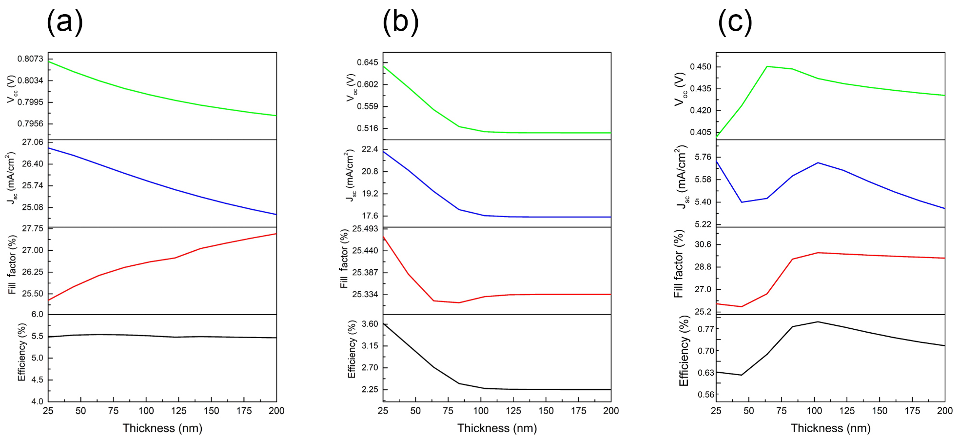
To determine the optimal buffer thickness, the calculations fixed the absorber thickness at 800 nm and the hole transport layer thickness at 100 nm, and shunt and series resistances were fixed in 26.8 Ω·cm2 and 103 Ω·cm2, respectively. From Figure 2a (radiative recombination mechanism), we can observe a few variations in the efficiency, around 5.5%, from 25 nm to 200 nm CdS thickness. For the fill factor the values ranged from 25 to 27%, whereas for current density of short circuit the values were close to 26 to 24 mA/cm2, and finally, for the open circuit voltage the value was around 0.8 V, which was the best value for all loss mechanisms. On the order hand, from Figure 2b,c we can observe values below those mentioned above for interface recombination of around 2%, and for Shockley–Read–Hall mechanisms around 0.7% efficiency, and we can conclude the optoelectronic parameters were not dependent on the buffer thickness, but they could depend on the shunt and series resistances.

3.2. Impact of Buffer Thickness in CdS/SnSe/SnTe-Based Solar Cell with Ideal Resistances with Different Loss Mechanisms

Regarding the impact of the buffer thickness, ideal resistances were used, meaning 0 for series resistance and a high resistance for shunt resistance. The thickness of the absorber layer was fixed at 800 nm, and the hole transport layer was 100 nm. From Figure 3a, for the radiative mechanism, we can observe variations from 25 nm to 200 nm in the buffer layer, and the maximum efficiency was 25 nm with a value around 24.5%; meanwhile the maximum efficiency was around 24% for 50 nm, and this value decreased as the CdS thickness increased until a value of around 21% was reached. These were the maximum values for all the loss mechanisms; as we can observe in (b) and (c), the efficiency was around 19 to 13% for interfaces mechanisms and for SRH 1.6% to 2.2%. Using this mechanism we can conclude that the HTL did not help to increase the efficiency of the solar cell, and 50 nm is going to be the optimum thickness for the next studies; the reason is because synthetizing below the limit of 50 nm without causing macroscopic defects to CdS has been difficult for researchers. Conversely, thin films exhibiting a minimal thickness of 50 nm are achievable while demonstrating good optoelectronic characteristics [26,27].

3.3. Impact of the Absorber Thickness in CdS/SnSe/SnTe-Based Solar Cell with Representative Resistances

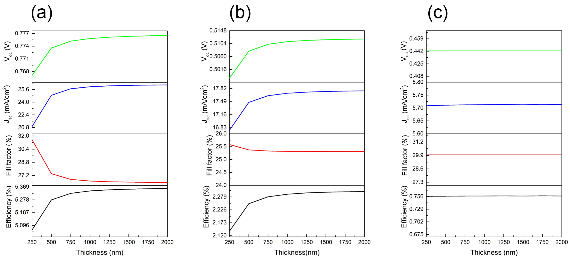
For analyzing the optimal absorber thickness, the buffer thickness was fixed at 100 nm, HTL thickness at 100 nm, and shunt and series resistances at 26.8 and 103 Ω·cm2, respectively, with the SnSe recombination value increasing. There are a few variations in SRH mechanisms. Thicknesses varied from 250 nm to 2000 nm. From Figure 4 it can be seen that as the absorber thickness increases, the Voc and Jsc values for two recombination mechanisms (which are interface and radiative) show an observable trend, and in the fill factor for the radiative and interface recombinations, there is a slight decrease in the values when the thickness increases. However, in SRH, no variation in the values is observed. There is a small efficiency increase in all the studies for values around 1250 nm, such as radiative recombination, with a value around 5.3% for the radiative mechanism, which is the highest value among the three recombination mechanisms.

3.4. Impact of the Absorber Thickness in CdS/SnSe/SnTe-Based Solar Cell with Ideal Resistances

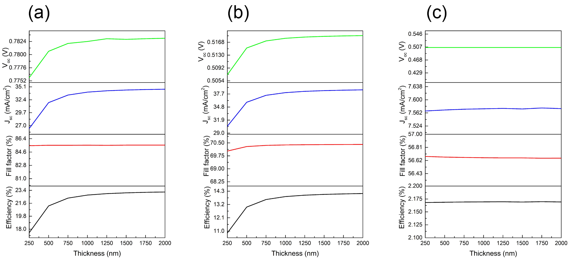
To ascertain the optimal thickness of the absorber material (see Figure 5), computations were executed utilizing a fixed buffer layer dimension of 100 nm and absorber layer thicknesses ranging from 250 nm to 2 mm. The consequence of both representative and ideal resistances pertaining to each recombination mechanism was duly considered. The initial noteworthy observation derived from the inspection of both conditions is that augmenting the thickness of the absorber material induces an increase in open circuit voltage and short circuit current density. Consequently, this enhances the efficiency when transport mechanisms such as radiative and interface recombination are the prevailing factors. Specifically, a minor fluctuation is detected under the interface recombination process, whereas when Shockley–Read–Hall (SRH) recombination is predominant, the characteristics of the photovoltaic device are virtually unaffected by thickness. This phenomenon is attributable to the significant influence of volumetric (bulk) defects on carrier mobility within this structural configuration, thereby impeding the photogenerated charge carriers from accessing the depletion region. A divergent tendency is observed pertaining to the fill factor of the solar photovoltaic device when considering both representative and ideal resistive parameters. When representative resistive parameters are incorporated into the computations, the augmentation in thickness yields elevated series resistances. This consequently diminishes Jsc and simultaneously the fill factor, as is evident under the radiative and interface recombination mechanisms. Nevertheless, when the influence of volumetric (bulk) defects, which constitute the primary source of carrier losses, is dominant, the fill factor remains unaffected by changes in the absorber layer thickness. Furthermore, a significant disparity is detected for Jsc under both radiative and interface recombination mechanisms. In the presence of representative resistances, diminished short-circuit current density values are procured for the interface recombination mechanism. Conversely, when resistive effects are disregarded, the Jsc magnitudes associated with both the radiative and interface mechanisms are found to be substantially equivalent. This finding demonstrates that the resistive losses are attributable to the materials themselves and the semiconductor/metal contact, rather than losses occurring at the CdS/SnSe interface. Generally, the open-circuit voltage exhibits a negligible deviation in response to alterations in the absorber layer thickness across all the transport mechanisms examined. These findings also substantiate that the subpar efficiency documented for the CdS/SnSe photovoltaic devices originates primarily from markedly low Jsc magnitudes. This deficiency is caused by the influence of SnSe bulk defects in conjunction with parasitic resistive losses. For subsequent computational work, a SnSe thickness of 1.25 mm is utilized, as the corresponding efficiency figures approximate their peak levels [28] (see Figure 5).

3.5. Impact of the Acceptor Density on Hole Transport Layer

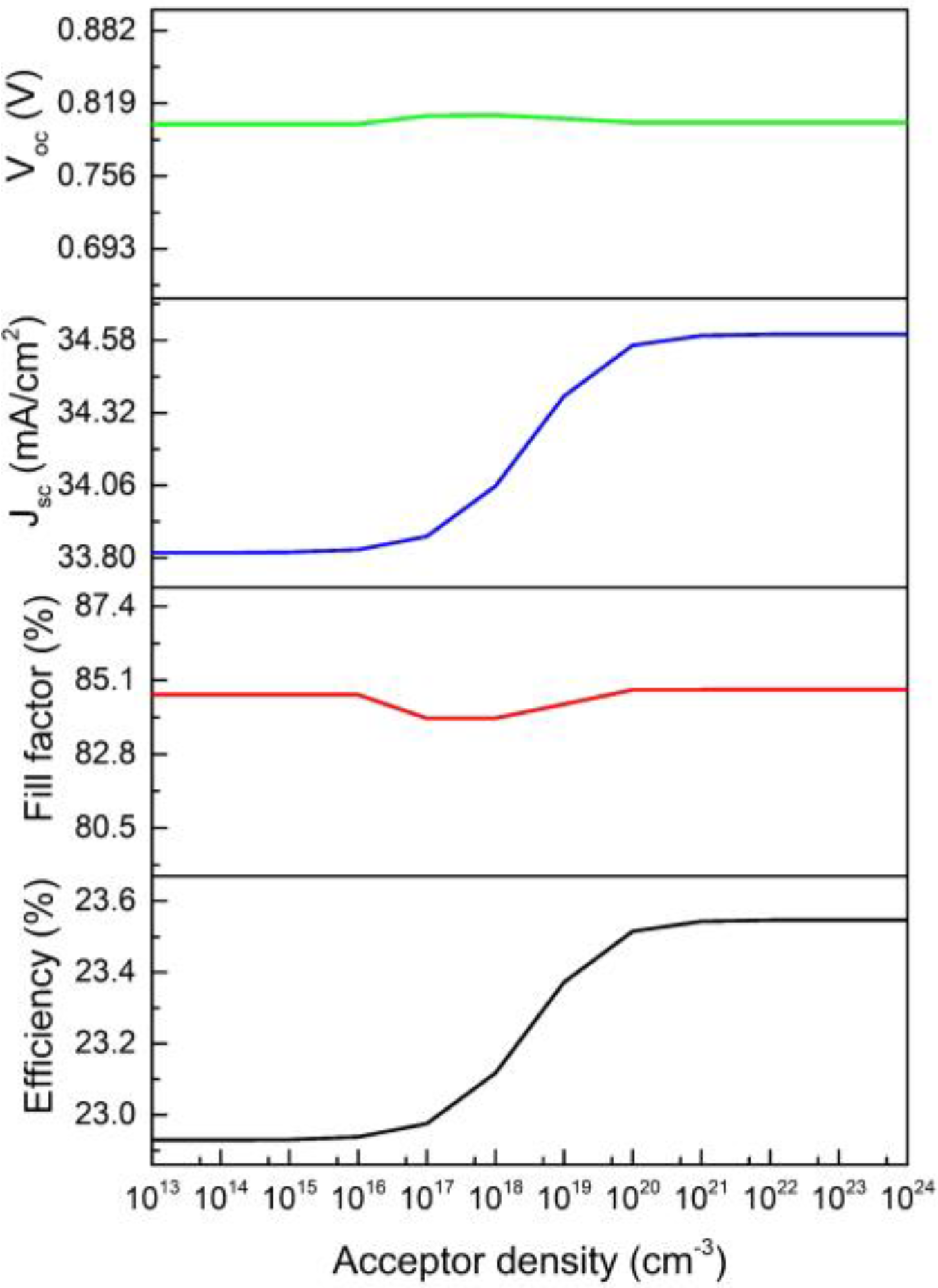
To find the optimal acceptor density for the solar cell, the buffer thickness was fixed at 50 nm, the SnSe layer at 1250 nm, and the HTL at 100 nm. The resistances were set to ideal values, the radiative recombination coefficients were fixed at 1 × 10⁻¹² cm3/s, the Nt were fixed at 1 × 1016 cm−3, the acceptor density at 1 × 1019 cm−3, and the interface defect density at 1 × 106 cm−2, following our previous work [21]. The acceptor density in SnTe varied from 1 × 10¹³ to 1 × 1024 cm−3. From Figure 6 it can be observed that the efficiency increases from approximately 23 to 23.5%, reaching its optimal value at 1 × 1020 cm−3. This improvement occurs because the SnTe material injects more holes in the base solar cell, thereby increasing the efficiency. For high values, the efficiency was almost constant, which could be attributed to defects in the absorber material or in the hole transport layer itself.
The inclusion of tin telluride, serving as a hole transport medium (HTL), markedly elevates the performance efficiency of solar cells predicated upon SnSe. One essential element involves the optimal alignment of the valence band maximum (VBM) between SnTe and SnSe [17], which establishes effective conductivity for hole extraction while concurrently mitigating interfacial energy impediments. This favorable arrangement significantly curtails recombination losses and is conducive to a higher open-circuit voltage. Furthermore, the superior hole mobility property inherent in SnTe plays a critical function in improving charge transfer kinetics. This inherent characteristic considerably diminishes the series impedance within the photovoltaic device, thereby contributing to an improved short-circuit current density. Furthermore, the establishment of a robust SnTe/SnSe interface mitigates defects sites and charge carrier confinement, culminating in superior charge removal efficiency. The supportive optical characteristics of SnTe facilitate enhanced solar spectrum harvesting, thereby boosting the photogeneration of charge carriers. Furthermore, the establishment of a robust SnTe/SnSe interface mitigates defects states and charge carrier trappings. This process culminates in superior charge removal PCE. The supportive optical characteristics of SnTe facilitate enhanced solar spectrum harvesting, thereby boosting the photogeneration of charge carriers [6].

3.6. Impact of the Bulk Defects on Hole Transport Layer

Using the parameters obtained in the previous section, the defects in the bulk of the SnTe material then varied from 1 × 10¹³ to 1 × 1020 cm−3. In Figure 7 it is shown that all of the optoelectronic parameters were constant, which is because all the loss mechanisms occur in the SnSe layer, and this observation is addressed in the next section.

3.7. Impact of the Acceptor Density on the SnSe

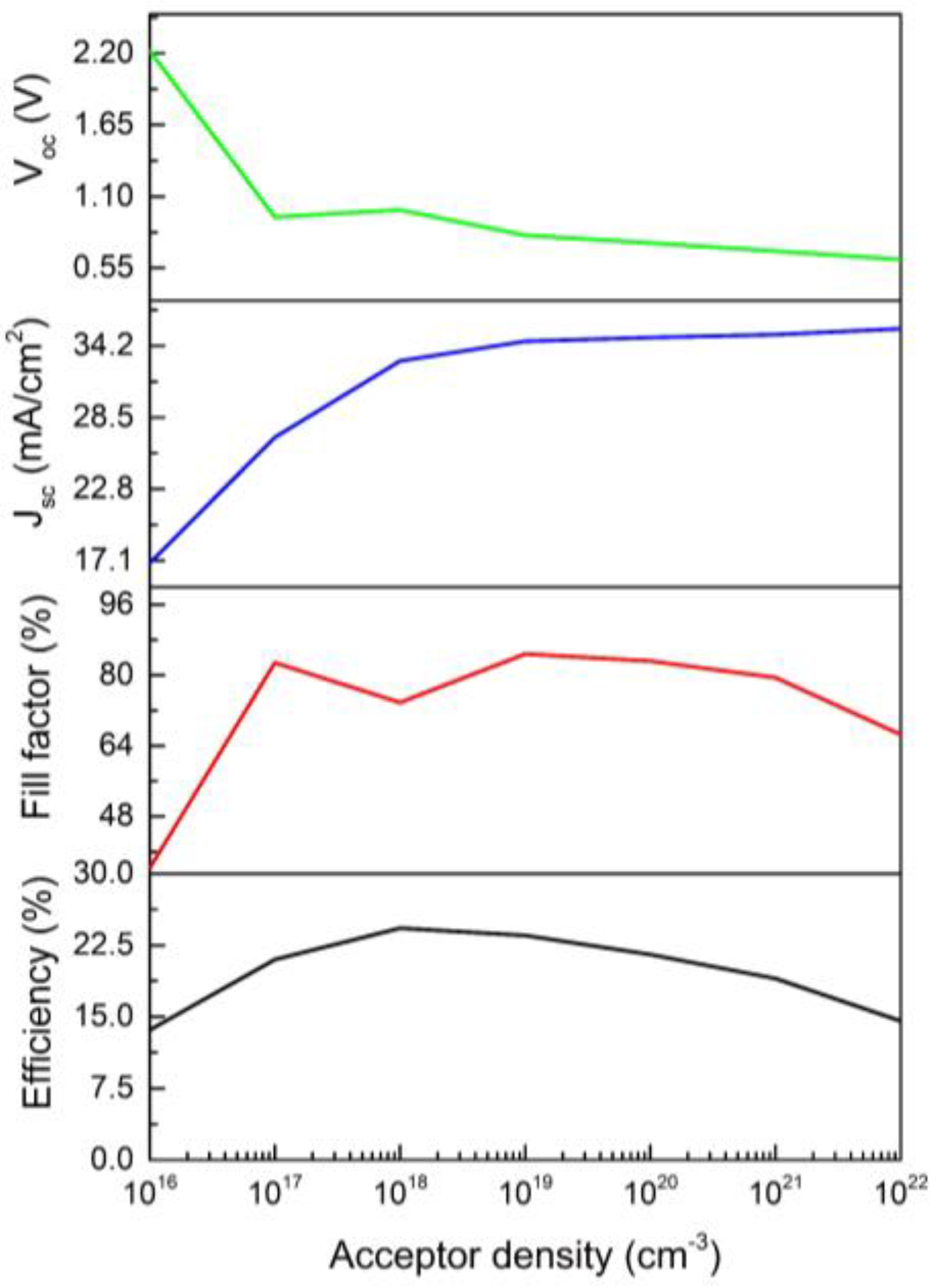
Acceptor density within absorber layer is a crucial factor that influences the performance of the solar cell. Enhancing the doping concentration is a crucial factor in the performance of the solar cell. SnSe acceptor density varied from 1016 to 1022 cm−3, as shown in Figure 8. At a density value of 1016 cm−3, Voc tends to decrease until 1022 cm−3, while the short circuit density begins with a low value and increases to a maximum value, and after 1019 cm−3 it begins to decrease. The fill factor (FF) commences with diminished values at a concentration of 1016 cm−3, remains stable throughout the range from 1017 up to 1020 cm−3, and subsequently begins to decrease. Finally, the efficiency exhibits initial low values, increases progressively to attain a peak value at 1019 cm−3, and subsequently commences to diminish, a finding that is in agreement with [29,30].

3.8. Impact of the Defects in Bulk on the SnSe

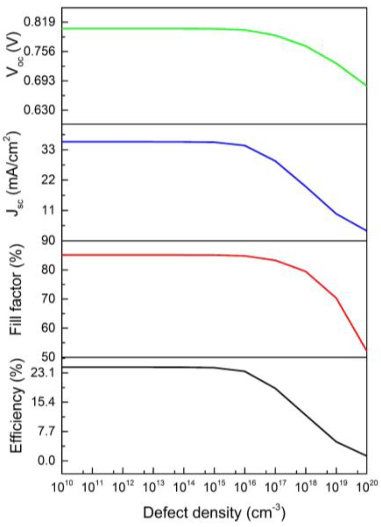
To optimize the solar cell, all the parameters found in the previous sections were employed. Finally, the defects in the absorber material can be analyzed (see Figure 9), which varied from 1 × 10¹⁰ to 1 × 1020 cm−3. The highest efficiency, around 24.48%, was achieved at 1 × 1015 cm−3 (see Figure 9).

3.9. Photovoltaic Characteristics of the Optimized Device

The J-V curves of both the optimized solar cell and the optimized cell using HTL (see Figure 10) were calculated for comparison. Voc is approximately 0.79 V for the cell without HTL and 0.81 V for the cell with HTL, while the Jsc is around 32 mA/cm2 for the cell without HTL and 35 mA/cm2 for the cell with HTL. The fill factor is 84.21% without and 85.09% with HTL. All of these optoelectronic parameters are below the S-Q limit. In this work, the inclusion of HTL increased the efficiency to around 14.8% (see Figure 10).

4. Conclusions

In this study, different loss mechanisms were analyzed as a function of the buffer and absorber thicknesses. It was observed that the SRH recombination is the mechanism that most negatively affects the optoelectronic parameter of the solar cell. Even with the inclusion of a HTL, no significant changes were observed compared to the base solar cell. The absorber thickness could be reduced from 1.7 to 1.25 μm, while the CdS buffer layer was maintained at 50 nm. In the study of the acceptor concentration, we observed that an increased hole density in the absorber improves the solar cell efficiency, which is expected because the HTL injects holes in the absorber material and reduces the recombination velocity. Bulk defects in SnTe did not significantly affect the optoelectronic parameters, likely because the dominant loss mechanisms occurs within the absorber. Finally, it was found that with an absorber defect density of 1015 cm−3 and an acceptor concentration of 1019 cm−3, the solar cell achieves a maximum efficiency of 24.48%.

Author Contributions

Conceptualization F.J.S.-R.; methodology, J.G.O.-I. and F.J.S.-R.; software; validation, F.J.S.-R., J.G.O.-I., A.C.-O., A.B.-V. and M.C.; formal analysis, F.J.S.-R., J.G.O.-I. and A.C.-O.; Investigation, F.J.S.-R., J.G.O.-I., L.N.I.-C., J.P.R.-L., I.M.d.l.S., J.J.M.-D., S.M.-A., F.R.-B. and M.C.; resources, L.N.I.-C., J.P.R.-L. and M.C.; data curation, F.J.S.-R., J.G.O.-I., A.C.-O., L.N.I.-C. and J.P.R.-L., J.J.M.-D., S.M.-A., F.R.-B. and M.C.; writing—original draft F.J.S.-R.; writing—review and editing, F.J.S.-R., J.G.O.-I., A.C.-O., A.B.-V., L.N.I.-C., J.P.R.-L., I.M.d.l.S., J.J.M.-D., S.M.-A., F.R.-B. and M.C.; resources, L.N.I.-C., J.P.R.-L. and M.C.; visualization F.J.S.-R., J.G.O.-I., A.C.-O. and M.C.; supervision, F.J.S.-R., J.G.O.-I., A.C.-O., A.B.-V., L.N.I.-C., J.P.R.-L., I.M.d.l.S. and M.C.; project administration, F.J.S.-R. and M.C.; funding acquisition, F.J.S.-R. and M.C. All authors have read and agreed to the published version of the manuscript.

Funding

This research received no external funding.

Institutional Review Board Statement

Not applicable.

Informed Consent Statement

Not applicable.

Data Availability Statement

The original contributions presented in this study are included in the article. Further inquiries can be directed to the corresponding author(s).

Acknowledgments

The authors thank Marc Burgelman of Ghent University, Belgium, for generously providing the SCAPS program.

Conflicts of Interest

The authors declare no conflicts of interest.

References

  1. Kumar, M.; Rani, S.; Singh, Y.; Gour, K.S.; Singh, V.N. Tin-selenide as a futuristic material: Properties and applications. RSC Adv. 2021, 11, 6477–6503. [Google Scholar] [CrossRef]
  2. Minnam Reddy, V.R.; Gedi, S.; Pejjai, B.; Park, C. Perspectives on SnSe-based thin film solar cells: A comprehensive review. J. Mater. Sci. Mater. Electron. 2016, 27, 5491–5508. [Google Scholar] [CrossRef]
  3. Shi, W.; Gao, M.; Wei, J.; Gao, J.; Fan, C.; Ashalley, E.; Li, H.; Wang, Z. Tin selenide (SnSe): Growth, properties, and applications. Adv. Sci. 2018, 5, 1700602. [Google Scholar] [CrossRef] [PubMed]
  4. Rühle, S. Tabulated values of the Shockley—Queisser limit for single junction solar cells. Sol. Energy 2016, 130, 139–147. [Google Scholar] [CrossRef]
  5. Mathews, N.R. Electrodeposited tin selenide thin films for photovoltaic applications. Sol. Energy 2012, 86, 1010–1016. [Google Scholar] [CrossRef]
  6. Barrios-Salgado, E.; Nair, M.T.S.; Nair, P.K. Chemically deposited SnSe thin films: Thermal stability and solar cell application. ECS J. Solid State Sci. Technol. 2014, 3, Q169. [Google Scholar] [CrossRef]
  7. Shinde, D.V.; Min, S.K.; Sung, M.M.; Shrestha, N.K.; Mane, R.S.; Han, S.H. Photovoltaic properties of nanocrystalline SnSe-CdS. Mater. Lett. 2014, 115, 244–247. [Google Scholar] [CrossRef]
  8. Li, Z.; Guo, Y.; Zhao, F.; Nie, C.; Li, H.; Shi, J.; Liu, X.; Jiang, J.; Zuo, S. Effect of film thickness and evaporation rate on co-evaporated SnSe thin films for photovoltaic applications. RSC Adv. 2020, 10, 16749–16755. [Google Scholar] [CrossRef]
  9. Abd El-Rahman, K.F.; Darwish, A.A.A.; El-Shazly, E.A.A. Electrical and photovoltaic properties of SnSe/Si heterojunction. Mater. Sci. Semicond. Process. 2014, 25, 123–129. [Google Scholar] [CrossRef]
  10. Kumar, M.; Rani, S.; Singh, Y.; Kumar, A.; Singh, V. Strategy to improve the efficiency of tin selenide based solar cell: A path from 1.02 to 27.72%. Sol. Energy 2022, 232, 146–153. [Google Scholar] [CrossRef]
  11. Jayan, K.D. Enhancement of efficiency of (FA)2BiCuI6 based perovskite solar cells with inorganic transport layers. Opt. Mater. 2021, 122, 111671. [Google Scholar] [CrossRef]
  12. Hashmi, G.; Hossain, M.S.; Rashid, M.J. Simulation of CdTe, CIGS and CZTS Solar Cells Using WxAMPS Software. Res. Square 2021. [Google Scholar] [CrossRef]
  13. Zyoud, S.H.; Zyoud, A.H.; Ahmed, N.M.; Prasad, A.R.; Khan, S.N.; Abdelkader, A.F.I.; Shahwan, M. Numerical Modeling of High Conversion Efficiency FTO/ZnO/CdS/CZTS/MO Thin Film-Based Solar Cells: Using SCAPS-1D Software. Crystals 2021, 11, 1468. [Google Scholar] [CrossRef]
  14. Faisal, S.; Rahman, S.I.; Ahmed, S.; Dhrubo, T.I. Numerical analysis of Mo Te2 thin film solar cell with Cu2Te BSF layer. In Proceedings of the TENCON 2017—2017 IEEE Region 10 Conference, Penang, Malaysia, 5–8 November 2017; pp. 2342–2346. [Google Scholar] [CrossRef]
  15. Gagandeep; Singh, M.; Kumar, R. Simulation of perovskite solar cell with graphene as hole transporting material. AIP Conf. Proc. 2019, 2115, 030548. [Google Scholar] [CrossRef]
  16. Xu, R.; Zou, X.; Liu, B.; Cheng, H.M. Computational design and property predictions for two-dimensional nanostructures Mater. Today 2018, 21, 391–418. [Google Scholar] [CrossRef]
  17. Kareem, M.Q.; Alimardan, S.S.; Mohammad, W.M.; Khudhair, I.M. Tailoring ETL/HTL combinations for high-performance ITO/i-ZnO/ZnS/SnSe/SnTe solar cells: A simulation approach. Results Surf. Interfaces 2025, 18, 100411. [Google Scholar] [CrossRef]
  18. Basore, P.A. Numerical modeling of textured silicon solar cells using PC-1D. IEEE Trans. Electron Devices 1990, 37, 337–343. [Google Scholar] [CrossRef]
  19. Gummel, H.K. A self-consistent iterative scheme for one-dimensional steady state transistor calculations. IEEE Trans. Electron. Devices 1964, 11, 455–465. [Google Scholar] [CrossRef]
  20. Burgelman, M. In Thin Film Solar Cells Fabrication, Characterization and Applications; Poortmans, J., Arkhipov, V., Eds.; Cadmium Telluride Thin Film Solar Cells: Characterization, Fabrication and Modeling. John Wiley & Sons Ltd.: West Sussex, UK, 2006; pp. 227–314. [Google Scholar]
  21. Kumari, R.; Kumar, R.; Singh, V.N. SnTe as a BSF enhances the performance of Sb2Se3 based solar cell: A numerical approach. Heliyon 2022, 8, e12043. [Google Scholar] [CrossRef]
  22. Dey, M.; Dey, M.; Matin, M.A.; Amin, N. Design of high performance and ultra-thin CdTe solar cells with SnTe BSF from numerical analysis. In Proceedings of the 18th International Conference on Computer and Information Technology (ICCIT), Dhaka, Bangladesh, 21–23 December 2015; pp. 573–576. [Google Scholar] [CrossRef]
  23. Im, H.S.; Myung, Y.; Cho, Y.J.; Kim, C.H.; Kim, H.S.; Back, S.H.; Jung, C.S.; Jang, D.M.; Lim, Y.R.; Park, J.; et al. Facile phase and composition tuned synthesis of tin chalcogenide nanocrystals. RSC Adv. 2013, 3, 10349. [Google Scholar] [CrossRef]
  24. Sa̧fak, H.; Merdan, M.; Yüksel, O.F. Dispersion analysis of SnS and SnSe. Turkish J. Phys. 2002, 26, 341–347. [Google Scholar]
  25. Ho, C.H.; Lin, W.Y.; Chao, L.C.; Lee, K.Y.; Inagaki, J.; Hsueh, H.C. Study of structural, thermoelectric, and photoelectric properties of layered tin monochalcogenides SnX (X = S, Se) for energy application. ACS Appl. Energy Mater. 2020, 3, 4896–4905. [Google Scholar] [CrossRef]
  26. Vigil-Galán, O.; Andrade-Arvizu, J.A.; Courel-Piedrahita, M.; Mejía-García, C.; Valencia-Resendíz, E.; Sánchez-González, Y.; Espíndola-Rodríguez, M.; Saucedo-Silva, E.; González-Castillo, R.; Rodríguez-González, E.; et al. Study of CBD-CdS/CZTGSe solar cells using different Cd sources: Behavior of devices as a MIS structure. J. Mater. Sci. Mater. Electron. 2017, 28, 18706–18714. [Google Scholar] [CrossRef]
  27. Vigil-Galán, O.; Pulgarín, F.A.; Cruz-Gandarilla, F.; Courel, M.; Villarreal-Ruiz, G.; Sánchez, Y.; Jiménez-Olarte, D.; Saucedo, E. Optimization of CBD-CdS physical properties for solar cell applications considering a MIS structure. Mater. Des. 2016, 99, 254–261. [Google Scholar] [CrossRef]
  28. Carrillo-Osuna, A.; Sánchez-Rodríguez, F.J.; Rodriguez-Osorio, K.G.; De Los Santos, I.M.; Morán-Lázaro, J.P.; Ojeda-Martínez, M.; Pérez, L.M.; Laroze, D.; Courel, M. Towards the CdS/SnSe solar cell optimization: Understanding the transport mechanisms. Results Phys. 2024, 67, 108035. [Google Scholar] [CrossRef]
  29. Pallavolu, M.R.; Minnam Reddy, V.R.; Guddeti, P.R.; Park, C. Development of SnSe thin films through selenization of sputtered Sn-metal films. J. Mater. Sci. Mater. Electron. 2019, 30, 15980–15988. [Google Scholar] [CrossRef]
  30. Labiod, A.; Khadir, A. Numerical Investigation of Advanced Thin-Film Solar Cells Based on SnSe. Acta Phys. Pol. A 2025, 147, 21. [Google Scholar] [CrossRef]
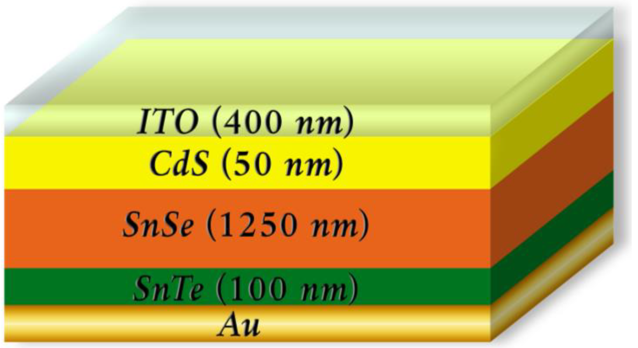
Figure 1. Schematic figure of the CdS/SnSe/SnTe solar cell.
Coatings 15 01324 g001
Figure 2. Studies on the impact of buffer thickness with representative resistances: (a) radiative recombination, (b) interface recombination, and (c) SRH recombination mechanisms.
Coatings 15 01324 g002
Figure 3. Optimization of CdS thickness with ideal resistances: (a) radiative recombination, (b) interface recombination, and (c) SRH recombination mechanisms.
Coatings 15 01324 g003
Figure 4. Studies on the thickness of SnSe with representative resistances: (a) radiative recombination, (b) interface recombination, and (c) SRH recombination mechanisms.
Coatings 15 01324 g004
Figure 5. Analysis of the thickness in SnSe with ideal resistances: (a) radiative recombination, (b) interface recombination, and (c) SRH recombination mechanisms.
Coatings 15 01324 g005
Figure 6. Acceptor density in SnTe.
Coatings 15 01324 g006
Figure 7. Defects in bulk in SnTe.
Coatings 15 01324 g007
Figure 8. Acceptor density in SnSe.
Coatings 15 01324 g008
Figure 9. Defects in the bulk in SnSe.
Coatings 15 01324 g009
Figure 10. Optimized without HTL vs. optimized with HTL.
Coatings 15 01324 g010
Table 1. Optoelectronic and geometric properties of the CdS/SnSe/SnTe solar cell; for SnTe, the parameters were taken from [21,22].
ParametersHTLLayer
SnTeSnSeCdSITO
Thickness, t (nm)100800100400
Band gap, Eg (eV)0.181.2 2.453.65
Electron affinity, χ (eV)5.14.1 [23]4.44.8
Dielectric permittivity, ε (relative)1009.94 [24]108.9
Effective density of states in the conduction band (CB-DOS), Nc (1/cm3)10161.96 × 10192.2 × 10185.2 × 1018
Effective density of states in the valence band (VB-DOS), Nv (1/cm3)10173.8 × 10181.8 × 10191.0 × 1018
Electron thermal velocity (cm/s)1077.3 × 1061 × 1071 × 107
Hole thermal velocity (cm/s)1071.25 × 1071 × 1071 × 107
Electron mobility, µn (cm2/Vs)50012510010
Hole mobility, µp (cm2/Vs)2720371 [25]5010
Shallow donor density, ND (1/cm3)001 × 10171 × 1017
Shallow acceptor density, NA (1/cm3)1 × 10181 × 101700
Disclaimer/Publisher’s Note: The statements, opinions and data contained in all publications are solely those of the individual author(s) and contributor(s) and not of MDPI and/or the editor(s). MDPI and/or the editor(s) disclaim responsibility for any injury to people or property resulting from any ideas, methods, instructions or products referred to in the content.