Article

Optimization of Gold Thin Films by DC Magnetron Sputtering: Structure, Morphology, and Conductivity

by
Wojciech Bulowski
1,2,*,
Katarzyna Skibińska
2,
Piotr Żabiński
2 and
Marek Wojnicki
2
1
CBRTP SA Research and Development Center of Technology for Industry, Ludwika Waryńskiego 3A, 00-645 Warszawa, Poland
2
Faculty of Non-Ferrous Metals, AGH University of Krakow, Al. Mickiewicza 30, 30-059 Kraków, Poland
*
Author to whom correspondence should be addressed.
Coatings 2025, 15(11), 1240; https://doi.org/10.3390/coatings15111240
Submission received: 27 September 2025 / Revised: 19 October 2025 / Accepted: 21 October 2025 / Published: 24 October 2025
(This article belongs to the Special Issue Thin Films and Nanostructures for Electronics)

Abstract

Gold thin films were deposited on quartz substrates by DC magnetron sputtering to fabricate electrodes for electrochemical and resistive sensing applications. The influence of sputtering parameters on film thickness, structure, and electrical properties was systematically investigated. XRD analysis revealed a predominant (111) crystallographic orientation. Microstrain values, determined via Williamson–Hall (W–H) analysis, were low (below 0.013) and closely correlated with surface roughness trends. AFM measurements showed that the surface roughness increased with film thickness. Electrical resistivity decreased linearly with increasing thickness and exhibited a critical grain size of approximately 25 nm, beyond which conductivity improved markedly. These results demonstrate the strong dependence of Au thin-film morphology and performance on deposition conditions, offering practical guidelines for optimizing their application in functional sensing devices.

1. Introduction

In electrochemical research and sensor development, the choice of electrode material is critical to both performance and reproducibility. Gold, despite its status as a noble metal, exhibits remarkably low catalytic activity toward many redox couples—minimizing unwanted side reactions [1,2]—while offering exceptional resistance to corrosion [3,4] and surface fouling [3]. These properties make gold an ideal substrate for studying intrinsic electrochemical processes, without interference from the electrode itself.
Equally important in producing reliable gold electrodes is the precise control of the film thickness [5]. Variations in layer thickness can alter surface roughness, electrical resistance, and active surface area, all of which directly impact measurement repeatability. In resistive gas sensors, the electrical contacts play a pivotal role in ensuring accurate signal transduction: if the gold layer deposited at the contact interface is too thin, its sheet resistance rises dramatically, introducing an additional, variable resistance in series with the sensing element and thereby skewing the measured output. Conversely, overly thick gold films drive up material costs. As a result, one must carefully optimize the gold coating thickness to strike the optimal balance between electrical performance and economic feasibility.
Achieving this balance involves not only precise control of deposition parameters—such as sputtering power and substrate rotation—but also predictive modeling of how film thickness influences both contact resistance and overall sensor characteristics. By targeting a gold thickness just above the percolation threshold for low-resistance pathways, manufacturers can minimize contact-induced artifacts without incurring unnecessary material expenses. Furthermore, real-time monitoring techniques like quartz crystal microbalance feedback and postdeposition four-point probe measurements provide the closed-loop control that is necessary to reproducibly hit this “sweet spot” in industrial and research settings alike.
Modern PVD systems for DC magnetron sputtering often incorporate closed-loop feedback algorithms that monitor the deposition rate and the magnetron discharge conditions in real time, enabling the operator to achieve the target thickness with only minimal deviation.
In resistive-sensor configurations, the quality of the electrical contact between the measurement probe and the sensing element is one of the foremost factors governing signal stability [6]. In impedance spectroscopy, in particular, uncontrolled contact resistance can be misinterpreted within equivalent-circuit models, leading to erroneous parameter extraction. By depositing gold films directly onto sensor contacts via DC magnetron sputtering, one can form a uniform, low-resistance interface that both enhances signal fidelity and ensures that observed variations arise from the sensing material itself, rather than from spurious contact effects.
Gold nanolayers exhibit thickness-dependent electrical conductivity. For instance, polycrystalline gold nanofilms with thicknesses ranging from 40.5 nm to 115.8 nm show variations in electrical conductivity that can be explained by the Mayadas and Shatzkes (MS) theory [7]. Additionally, gold thin films deposited on poly(vinyl chloride) substrates demonstrate increased DC conductivity with increasing thickness, from 20 nm to 100 nm [8]. Electrically continuous coverage is achieved at an average thickness of approximately 4 nm for PET (polyethylene terephthalate) and 5 nm for PTFE (polytetrafluoroethylene) substrates, leading to a rapid decrease in layer resistance with increasing sputtering time [9].
Studies suggest that there is an optimum thickness for achieving the best electrical properties. For instance, annealing increases both the dielectric constant and ac conductivity of the optimum Au thin film [10]. For the Au layers, dc sputtered on microscopic glass, a rapid decline in electrical sheet resistance occurs for sputtering times above 50 s [11]. The annealing, in air at 300 °C for 1 h, shifts the decline in electrical resistance to sputtering times above 250 s. A similar shift toward thicker layers is observed, for example, with a drop in volume resistivity or an increase in free carrier concentration [12]. This indicates that a continuous layer forms after a longer deposition time for annealed samples. Moreover, annealing in vacuum at moderate temperatures (175 °C and below) of Au films deposited via dc magnetron sputtering causes the lateral expansion of the grains and an increase in their size [13]. It results in a decrease in layer roughness.
Additionally, sputtered gold nanolayers (80 nm thick) exhibit electrochemical behavior of two selected probes (ferrocyanide/ferricyanide and hydroquinone/benzoquinone) that is comparable to those of gold bulk electrodes. They could be further improved with improvements to their fabrication process, e.g., prolonging the deposition time to synthesize a more compact layer [14]. DC sputtering of Au nanofilms on conductive substrates allows the production of electrodes for effective As (III) detection in water [15]. The proposed method enables the use of ultralow (<10 μg cm−2) loads of Au. At the same time, the ion-sputtered layer of Au significantly increased the response time and rate in the low-concentration NH3 detection [16]. Present gold enhances the catalytic activity of the anodic electrode reaction, thereby improving the sensor’s properties.
Zhaoqi Sun and others [17] deposited ultrathin Au films via dc magnetron sputtering, with different sputtering times. They investigated the changes in surface morphology, microstructure, and electrical properties by XRD, AFM, TEM, and the temperature-varying four-wire technique. They found that with the increase in deposition time, the layer thickness increases from 3.2 to 97.8 nm, and the average particle size increases from 22.1 to 54.3 nm. At the same time, the resistance decreases rapidly, while the film thickness changes (from 3.2 to 6.8 nm).
Simultaneously, many works focus on the annealing of Au after the dc magnetron sputtering [18,19,20].
The thickness of gold nanolayers has a significant impact on sensor performance, as well as on electrochemical behavior. In this study, three different process parameters were investigated, as each of them influences the deposition process:
Sputtering current—with the increase in sputtering current, the sputtering yield increases. More ions are generated and accelerated towards the target material, and more atoms are removed from the target surface. It leads to a faster deposition rate.
Deposition time—this does not influence the sputtering yield. With a longer deposition time, more ions are bombarding the target, so the total number of ejected atoms is greater, and a thicker film can be obtained, e.g., for CrN [21].
Target-substrate distance—shorter distance enhances the deposition rate, and the films with larger grains can be obtained [22]. At a higher distance, the deposition rate is slower, as sputtered atoms undergo more collisions with gas molecules. It is even more crucial at higher gas pressures [23]. At the same time, with the increase in target–substrate distance, the difference in particle concentration on the surface is lower, and the deposition uniformity is better [24].
Of course, thin gold layers could be deposited by other techniques, like RF (radio frequency) magnetron sputtering or thermal evaporation; however, such methods require more advanced equipment, like an RF generator, or have higher energy consumption due to a higher vacuum need or a high-temperature heating element.
RF sputtering produces layers with lower defect density and higher uniformity, albeit at lower deposition rates than DC magnetron sputtering. Moniruzzaman Syed et al. [25] demonstrated that a 40 nm gold film with low internal stress can be deposited at room temperature in 35 min, using RF magnetron sputtering, corresponding to a deposition rate of 0.19 Å/s, substantially lower than typical DC sputtering rates.
In the case of thermal evaporation systems, deposition rates are higher than magnetron sputtering, but because of the lack of protective noble gas (argon) and the high temperature element, which could cause co-evaporations, the purity of deposited layers are lower. Jan Kejzlar and others [26] used a thermal evaporation system to deposit gold layers on silicon substrates. Using 160 mg of gold and a heating current of 130 A in a time of 90 s, they deposited 747 ± 210 nm of gold on substrates. The proposed process resulted in a deposition rate of 83 ± 23 Å/s, but layers were highly contaminated by oxygen, carbon, and tungsten (respectively, 14, 31 and 2 at % by XPS technique).
In comparison to these two techniques, DC magnetron sputtering is a cheaper, easier, and faster way to obtain pure gold layers.
Together, these considerations underscore the need for a robust PVD approach to gold film fabrication—balancing the chemical inertness of the metal with stringent thickness control to meet the demands of advanced electrochemical studies and sensor technologies. We believe that our work comprehensively describes the influence of the DC magnetron sputtering on the structure, morphology, and conductivity of as-deposited Au thin films.

2. Materials and Methods

Gold targets (Ø 57 mm, 99.99% purity) were supplied by Mennica Metale Szlachetne (Radzymin, Poland). To minimize substrate-induced texture effects, all films were deposited onto optically polished quartz glass slides of 30 × 30 × 1 mm (Hellma, Müllheim, Germany). Before depositions, all glasses were cleaned using isopropanol and acetone, then rinsed with distilled water and treated with a plasma cleaning process for 5 min in 480 W oxygen plasma.
Depositions were carried out in an Emitech K575XD DC magnetron sputtering system with a rotating sample table (Quorum Technologies Ltd, East Grinstead, UK). After achieving a base pressure below 5 × 10⁻⁶ mbar, argon (99.999%) was introduced to a working pressure of 5 × 10⁻³ mbar. The gold target was driven at a constant current (varied between 25 mA and 100 mA), and the target–substrate distance was set between 29 mm and 35 mm, to explore its effect on the deposition rate. The deposition time varied from 4 to 16 min. No external substrate heating was applied.
The purity of deposited gold layers was investigated by the scanning electron microscope, Phenom Pharos (Thermo Fisher Scientific, Waltham, MA, USA), equipped with an SDD EDS (energy dispersive spectroscopy) sensor.
Surface topography and roughness (Ra and Rz) were mapped by atomic force microscopy (AFM) (NT-MDT Ntegra Prima, NSG01 probe, NT-MDT, Apeldoorn, The Netherlands) over 5 µm × 5 µm scan areas. Crystalline grain sizes were extracted from X-ray diffraction patterns (Rigaku Miniflex II spectrometer equipped with a copper tube, Rigaku, Tokyo, Japan), via the Scherrer equation. The intensity of Cu-Kα radiation was measured by the wavelength dispersive X-ray fluorescence (WDXRF) method on the spectrofluorometer, Rigaku Primini (Rigaku, Tokyo, Japan), using scintillation counters (LiF1 crystal).
For the resistivity measurement, the four-point probe method was used. Measurements were conducted at room temperature with the use of a soft-tipped four-point probe (Ossila, Sheffield, UK).
The sheet carrier concentrations and their mobility were measured by the Hall effect measurement system, ECOPIA HMS-5500 (Anyang, Republic of Korea), with a high temperature chamber, AHT55T5. Samples were measured in a nitrogen atmosphere at room temperature and elevated temperatures up to 773 K.
To estimate the thickness of the Au layer on the glass surface, the optical properties of the layer are considered. For this purpose, a laser ellipsometer SE 400adv PV was used (SENTECH, Berlin, Germany).
UV-Vis spectra were recorded using Jasco V680 (Jasco, Tokyo, Japan). Air was used as the reference material in the reference optical path.

3. Results and Discussion

3.1. Thickness and Chemical Composition

To eliminate the possibility of impurity’s influence on further analysis, the purity of deposited layers was examined. For composition measurements, energy dispersive spectroscopy techniques were used. Analyses were conducted on a 1.34 µm × 1.34 µm square of the sample, using 30 kV of accelerating voltage, a high-intensity electron beam, and the ZAF model for spectrum analysis; the time of collecting the spectrum was limited to 120 s (Figure S1). Chosen measurement parameters allowed us to collect above 3 million counts, which resulted in a good spectrum with low background noise and visible bands.
In accordance with the assumptions, the sample analyzed consists of nearly 100% gold, with only a very small amount of carbon impurities 0.32 wt. % (Table 1). Due to the high influence of the surface in EDS analysis, it can be assumed that all carbon signals come from organic surface impurities, which come from sample storage and not from the deposition process. Further EDS spectrum analysis can be found in the Supplementary Materials. The conducted analysis proves that during the deposition process, phenomena like co-evaporation, substrate diffusion to the layer, etc., did not occur, and deposited layers can be further investigated, like pure gold.
To evaluate the deposition rate of gold sputtering, a thickness measurement was conducted. The thickness of layers was calculated based on the weight change in substrates after deposition.
The proposed method is very easy and versatile; it acquires measurements, given the mean value of thickness from all substrate surfaces, and is free of topography influences, like roughness or reflexivity, which cause problems in other techniques like ellipsometry. A thickness evaluation based on weight change was used previously by Mech et al., to measure the thickness of the sputtered thin layer of copper [27].
d = m S u b m S u b A u S S u b ρ A u
where d—layer thickness [cm] (to convert to nanometers correcting coefficient 107 were used), msub and msubAu—weight of substrate and substrate with deposited gold [g], Ssub—surface of substrate [cm2], and ρAu—gold density [g/cm3].
For calculations, 9 cm2 was used for the surface of the substrate (quartz sliders dimensions 3 × 3 cm) and 19.32 g/cm3 was used as the gold density [28]. All calculation results were collected in Table 2.
Based on the obtained thickness data, the deposition rates for different process parameters were calculated and presented in Figure 1.
The deposition rate, calculated based on the mass of gold deposited on the substrate, shows a clear dependence on sputtering parameters. As expected, the deposition rate increases linearly with the applied current, rising from 1.82 Å/s at 25 mA to 9.15 Å/s at 100 mA (Figure 1a). In contrast, the variation in deposition time reveals a non-linear behavior: the sputtering rate reaches a maximum of 6.92 Å/s at 8 min and then decreases to 4.64 Å/s at 16 min (Figure 1b). Although these changes are less pronounced than those observed for the current, they may be attributed to thermal effects, such as gradual heating of the target or substrate during prolonged sputtering. Such heating could reduce the effective sputtering yield or enhance desorption processes, leading to a lower net material accumulation. However, the observed spread in the values appears to be largely statistical in nature, with an average sputtering rate of 6.08 ± 0.50 Å/s. Alternative explanations for this behavior cannot be excluded at this stage.
In addition to thermal effects, other factors may contribute to the reduced deposition rate at longer durations. These include changes in the surface morphology of the growing film, such as increased surface roughness or columnar growth, which can introduce shadowing effects and decrease the efficiency of incoming atom incorporation. Furthermore, long sputtering times may lead to partial re-deposition of sputtered atoms, or formation of re-sputtered layers that reduce the net accumulation of material. Fluctuations in the magnetron discharge stability over time or target surface modification (e.g., redeposition or surface poisoning) could also reduce the effective sputtering yield. These findings highlight the importance of both the current and deposition times in optimizing material transfer efficiency in magnetron sputtering, and underline the complex interplay of thermal and morphological factors during extended deposition processes [29,30].
The intensity of the Cu-Kα radiation measured in the WDXRF method can be connected with the thickness of the sample (the further discussion on WDXRF and thickness calculations from the intensity can be found in the Supplementary Materials). The dependency between the deposition parameters (deposition time, applied current, and target–substrate distance) and the intensity of Cu-Kα radiation is shown in Figure S2a–c. The intensity of the Cu-Kα radiation increases with the prolongation of the deposition time and with the increase in the applied current. However, there is no relationship between this intensity and the target-substrate distance.
The functions describing the dependence between the peak maximum and deposition conditions are shown in Figure S3. The higher the radiation intensity, the thicker the sample [31]. The obtained results allow us to assume that the thickness of the thin film increases linearly with the applied current, and exponentially with the prolongation of the deposition time. The distance between substrate and target has no significant effect on the samples’ thickness.
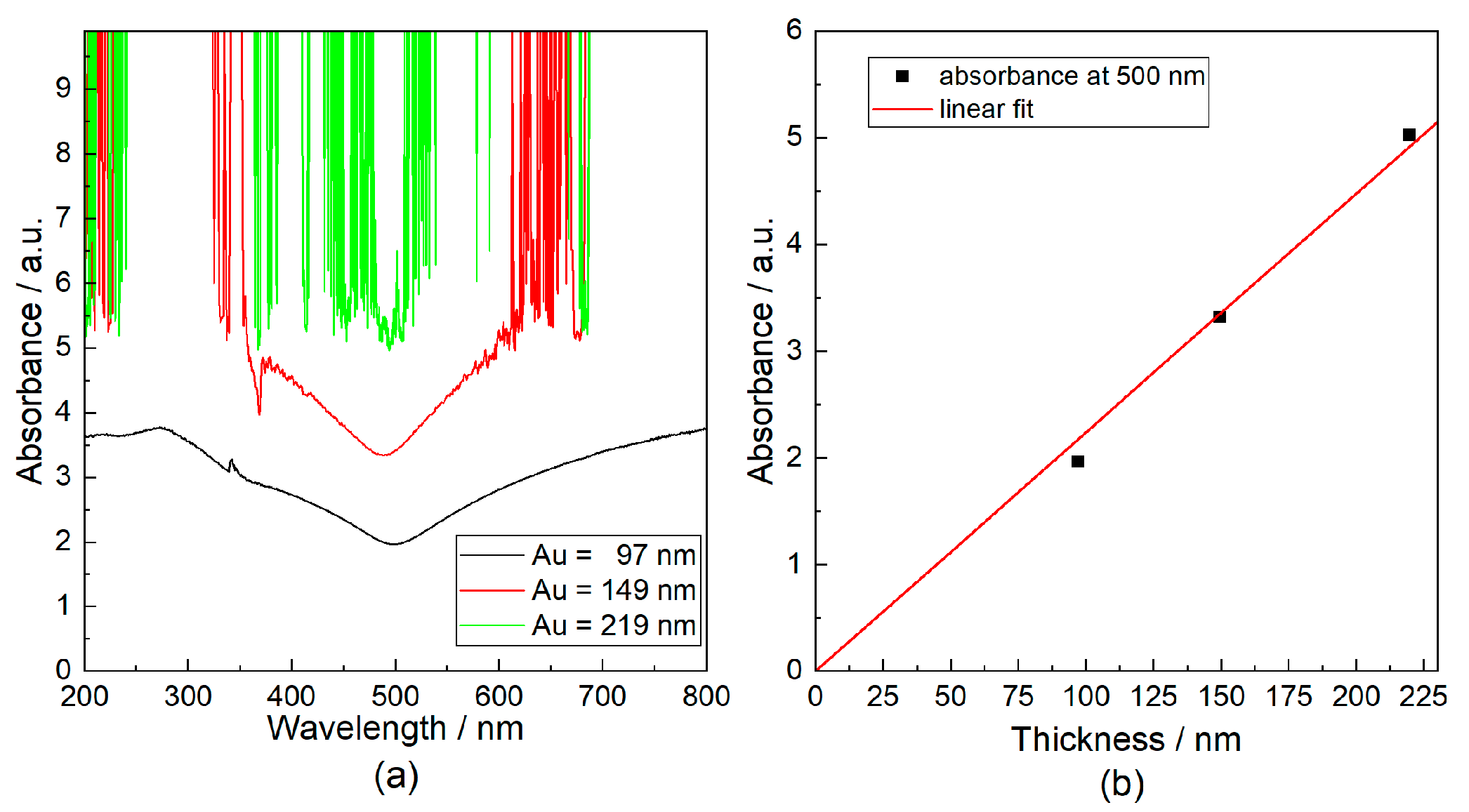
Then, the optical properties of the deposited gold thin films were investigated using UV-Vis spectroscopy. Absorbance spectra were recorded for a series of samples with varying gold layer thicknesses. As illustrated in Figure 2a, the spectra exhibit characteristic absorption bands, which are attributed to the surface plasmon resonance (SPR) of gold nanoparticles/films [32,33]. The intensity of this absorption is directly related to the amount of deposited gold.
To establish a quantitative relationship, the absorbance at a specific wavelength, λ = 500 nm, was plotted against the layer thickness. The thicknesses were independently determined by gravimetric analysis. As shown in Figure 2b, the relationship between absorbance and thickness is a linear function that passes through the origin. This observation is in excellent agreement with the Lambert–Beer law:
A = ε b c
where absorbance (A) is directly proportional to the path length (b, which in this case corresponds to the layer thickness) and the concentration of the absorbing species (c). The linear correlation confirms that the gravimetrically determined thicknesses form a consistent and reliable data set for optical analysis. The high correlation coefficient (R2 > 0.99) further underscores the precision and validity of this relationship.
Ellipsometry, a non-destructive optical technique, was also utilized to determine the thickness of the gold films. Measurements were performed using a SE 400adv PV ellipsometer, equipped with a 632.8 nm laser source. This method relies on analyzing the change in the polarization of light upon reflection from the sample surface.
However, as can be seen from the UV-Vis spectra in Figure 2a, the absorbance of gold films increases significantly with a thickness of 632.8 nm. For films with thicknesses exceeding approximately 100 nm, the absorbance is so high that the reflected signal becomes too weak to be accurately measured by the ellipsometer. Consequently, the applicability of this method is limited to thinner films, where the transparency of the layer allows for a sufficient reflected signal.
To validate the consistency of the different characterization methods, a specific sample was synthesized under controlled conditions and analyzed by multiple techniques. The key synthesis parameters for this sample were as follows. Current: 25 mA, distance: 35 mm, and time: 4 min.
The gold thickness calculated from the mass gain (gravimetric method) was 43.7 nm. The thickness of the same sample, as determined by ellipsometry, was 37.7 nm. The optical model used for the thickness measurement was air/2.5 nm roughness (1:1 air/gold ratio)/gold/Si<100>. The differences in measured values could come from quite high, but acceptable mean square fitting error: 2.5 (fitting of measurement data to the optical model), but also from other sources like substrate influence (in ellipsometry silicon <100> substrates were used) or a refractive index mismatch of the one used in the model to the real one (refractive index could vary a little due to roughness, structure, or internal stresses.)
While there is a slight discrepancy between these values, it is important to consider the factors influencing each measurement. Ellipsometry is known to be highly sensitive to film properties such as density, roughness, and internal strain. The presence of stress in the thin film, as indicated by a broadening of X-ray diffraction (XRD) peaks and confirmed by Wilson–Hall analysis, can influence the refractive index and lead to variations in the ellipsometrically determined thickness.
Considering this, the agreement between the gravimetric and ellipsometric measurements is considered to be excellent. This consistency, along with the correlation to other methods like wavelength dispersive X-ray fluorescence (WDXRF) intensity, which also scales with film thickness, demonstrates the robustness and reliability of the determined thickness values across various independent characterization techniques.

3.2. Structure

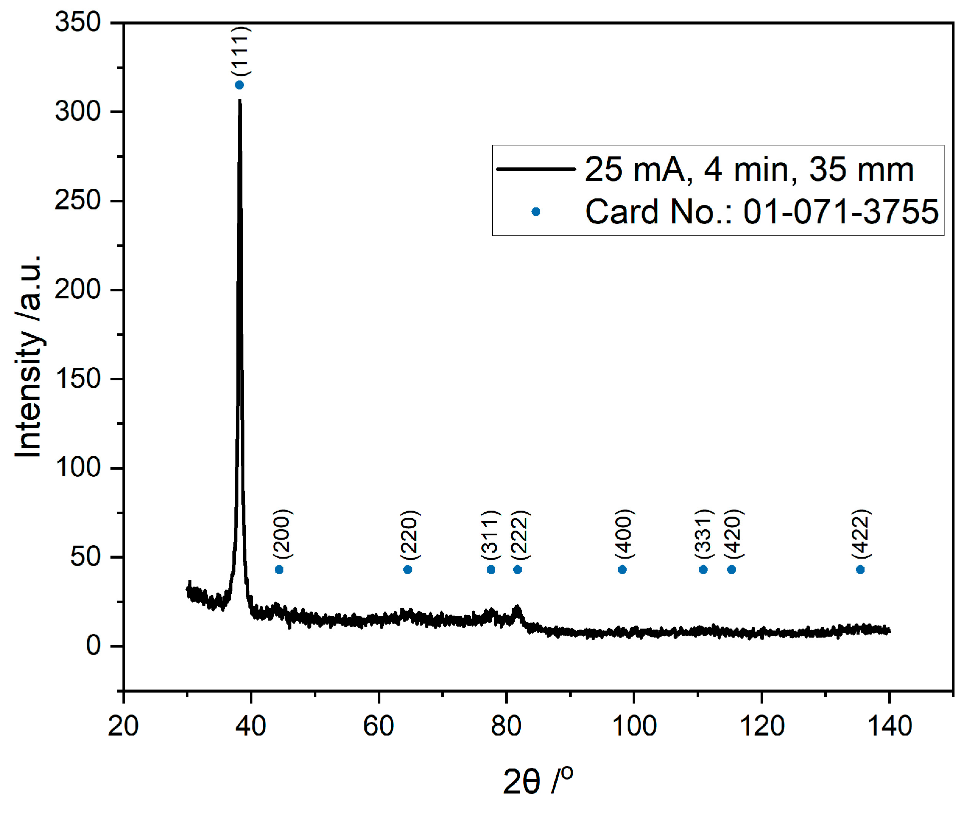
The deposition of gold (Au) using physical vapor deposition (PVD) techniques significantly influences the X-ray diffraction (XRD) patterns of the resulting films. The morphology of gold nanostructures, such as nanowires or thin films, can be influenced by the deposition conditions. XRD analysis reveals that these conditions affect the crystallinity and phase composition of the gold structures, which in turn modifies the XRD patterns [34,35]. The initial scan was performed from 30 to 140°, with a scan speed of 0.5°/min. The example of the XRD pattern for the gold thin film, deposited at 25 mA for 4 min with a target–substrate distance of 35 mm, is shown in Figure 3. Peaks corresponding to the cubic crystal structure are marked with blue dots (JCPDS, Card No.: 01-071-3755 Quality: I).
The thin film obtained exhibits a crystalline structure with the most intense dominant peak, corresponding to (111) preferred orientation. Therefore, scans in the range from 33 to 44° with a scan speed of 1°/min were performed to analyze the influence of the deposition parameters. They are shown in Figure S4. There is no clear trend between the value of intensity and the applied parameters (further discussion can be found in the Supplementary Materials).
The peak, corresponding to the (111) preferred orientation, was also used in calculations of crystalline grain size via the Scherrer Equation (3):
D   = K λ β c o s θ  
where K is a Scherrer constant (here 0.94), λ is a wavelength of the X-ray radiation used (0.15418 for Cu K-α), β is a full width at half maximum (FWHM) of the diffraction peak, and θ is a Bragg angle of the diffraction peak. Results of the calculations are listed in Table S1. Prolongation of the deposition time from 4 to 8 min increases the crystalline grain size. A longer deposition has a slight influence on the mentioned size. With the increase in the applied current from 25 mA to 75 mA, the grains increase in size. For 100 mA, they are a bit smaller again. Generally, sputtering current up to a certain value supports the grain growth, after which, the grain size can start to decrease due to the supersaturation [36]. There is no clear dependence between the target–substrate distance and the values of crystalline grain size.
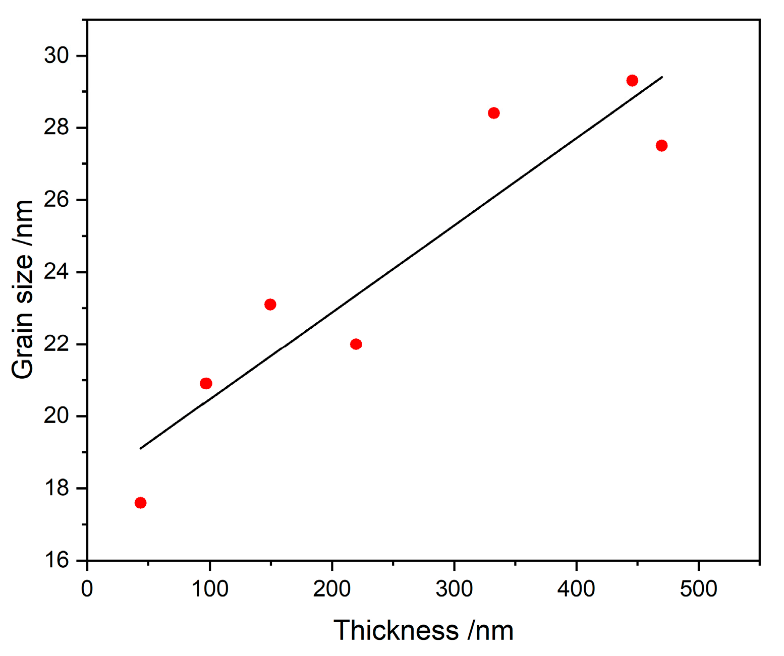
Additionally, calculated grains sizes were plotted against thickness (Figure 4).
A clear linear increase in grain size with film thickness is observed. This behavior can be attributed to the polycrystalline columnar growth of the gold layer, where grains coalesce and elongate as the film thickens. The increase in grain size suggests that thicker films have a lower grain-boundary density, which can influence electrical conductivity. Moreover, the linear trend indicates that the growth process is largely governed by competitive grain growth rather than nucleation of new grains, providing insight into the microstructural evolution of the deposited films.
To further examine the microstructure of deposited gold layers, the crystalline structure and microstrains were examined. To evaluate the microstrains, a Williamson–Hall (W–H) analysis was conducted.
β cos θ k λ = η 4 sin θ k λ + 1 d X R D
where β—full width at half maximum, θ—Bragg angle, λ—X-ray wavelength (0.15418 for Cu K-α), k—shape factor (0.94), d—volume-weighted crystallite size, and η—microstrains.
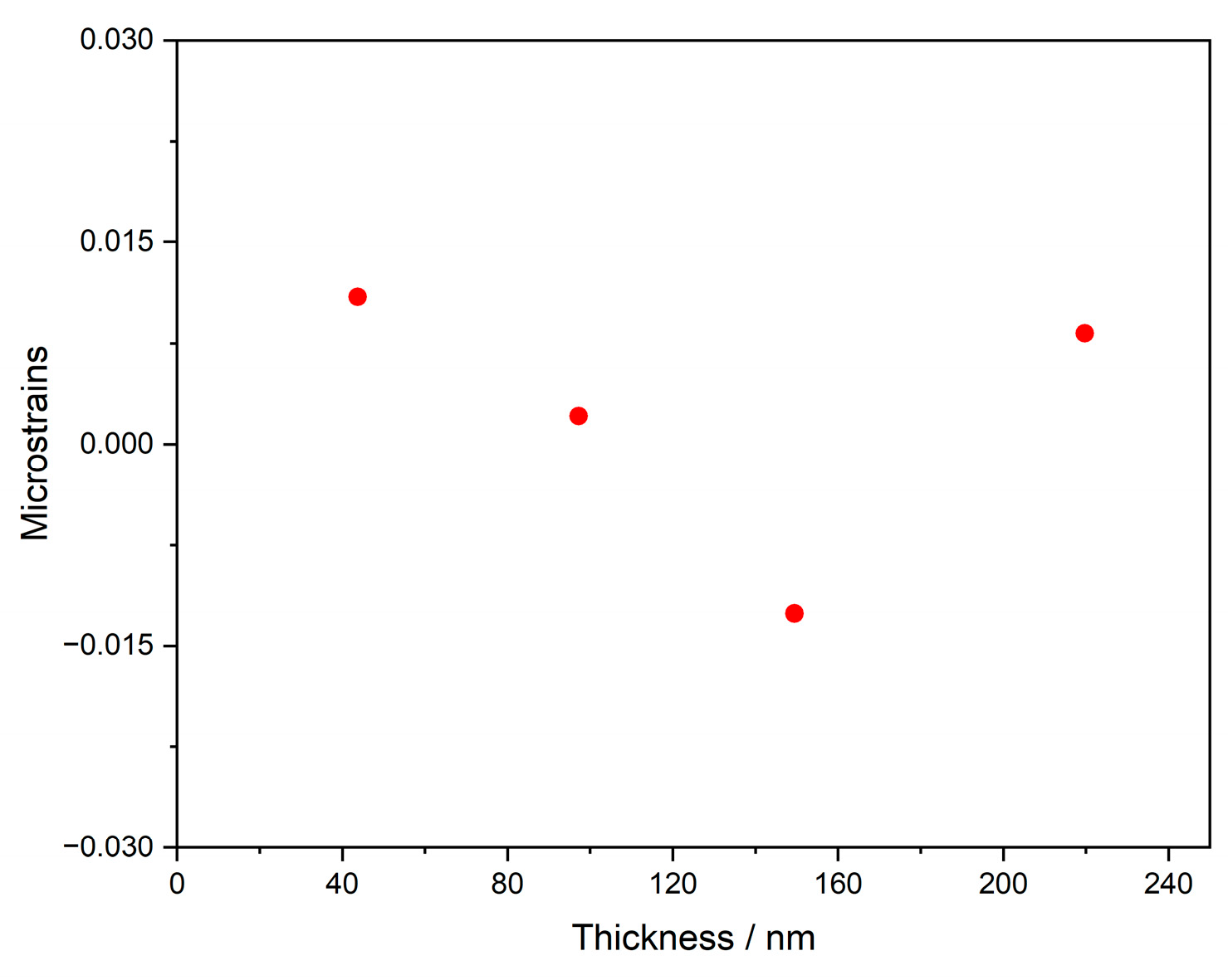
Using Equation (4), microstrains for four samples with different thicknesses were calculated and presented in Table 3.
The negative values of microstrains obtained from the W–H analysis indicate the presence of compressive lattice distortions, suggesting that during deposition, atoms are forced into positions slightly closer than their equilibrium spacing. This can arise from limited adatom mobility and atomic peening effects that are inherent to magnetron sputtering. Such compressive strain typically enhances film density and adhesion, but may also influence defect formation and stress–relaxation behavior as the film grows thicker.
The microstrain values obtained from the Williamson–Hall (W–H) analysis (Table 3) are relatively small: below 0.013. This is consistent with the magnetron sputtering process, where deposited films are usually free from significant lattice deformations, due to the absence of thermal stresses and the relatively low kinetic energy of the sputtered particles. The growth of the film in a columnar manner also reduces grain overcrowding at the substrate surface, which further minimizes strain [37,38]. Moreover, due to the directional nature of deposition, the XRD intensity of the (111) plane is much higher, when compared to other planes (Figure 3). As a consequence, the visibility of minor peaks is reduced, and therefore only four diffraction peaks were considered in the analysis.
As observed in Figure 5, the microstrain values in the analyzed layers exhibit a thickness-dependent variation that closely follows the trend of surface roughness parameters Ra and Rz. This parallel behavior suggests a potential correlation between microstrain and surface morphology: as the layer thickness increases, columnar growth and grain coalescence may enhance both surface roughness and lattice distortions.

3.3. Morphology

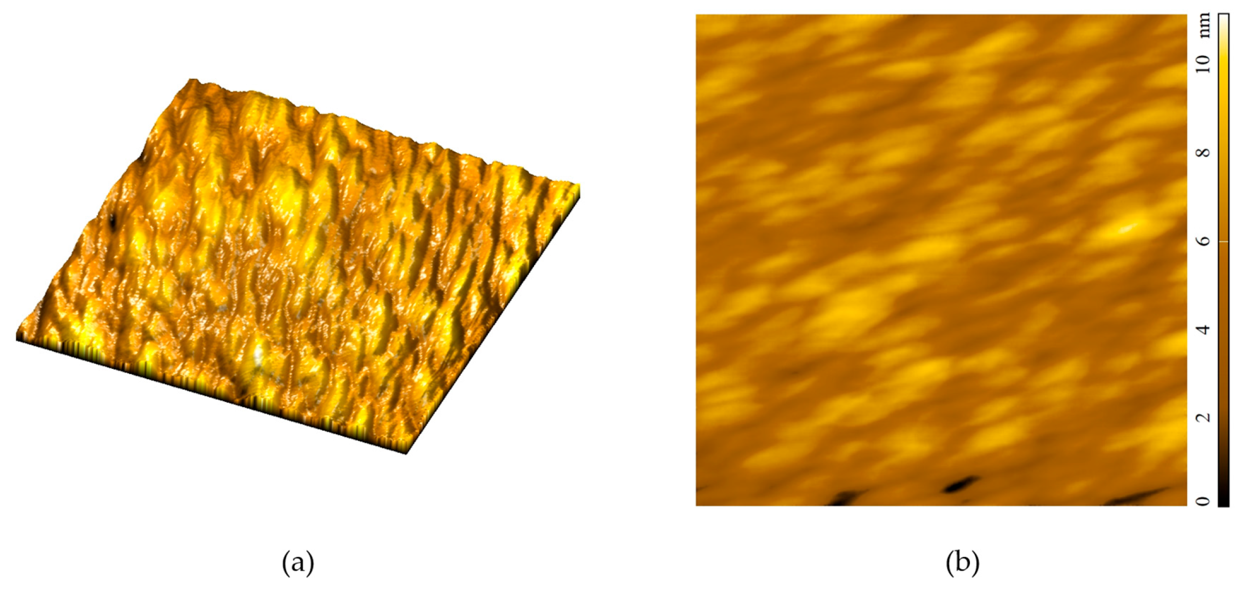
Thin gold layers deposited by techniques such as thermal evaporation of magnetron sputtering tend to form island films or pillar structures, rather than continuous conformal films [39,40]. To investigate the growth mechanism of gold layers, in our approach, AFM imaging combined with roughness analysis was implemented (Figure 6).
Figure 6. AFM image of layer deposited by magnetron sputtering (I = 100 mA, t = 4 min, L = 35 mm) for area 500 nm × 500 nm in 3D (a) and 2D (b).
Coatings 15 01240 g006
To prevent surface deformation due to the very low hardness of gold layers, acquisition of all images was conducted in semi-contact mode. Roughness analysis was conducted on an area of 5 µm × 5 µm, with the help of the statistics function of Nova 1.1.1 software.
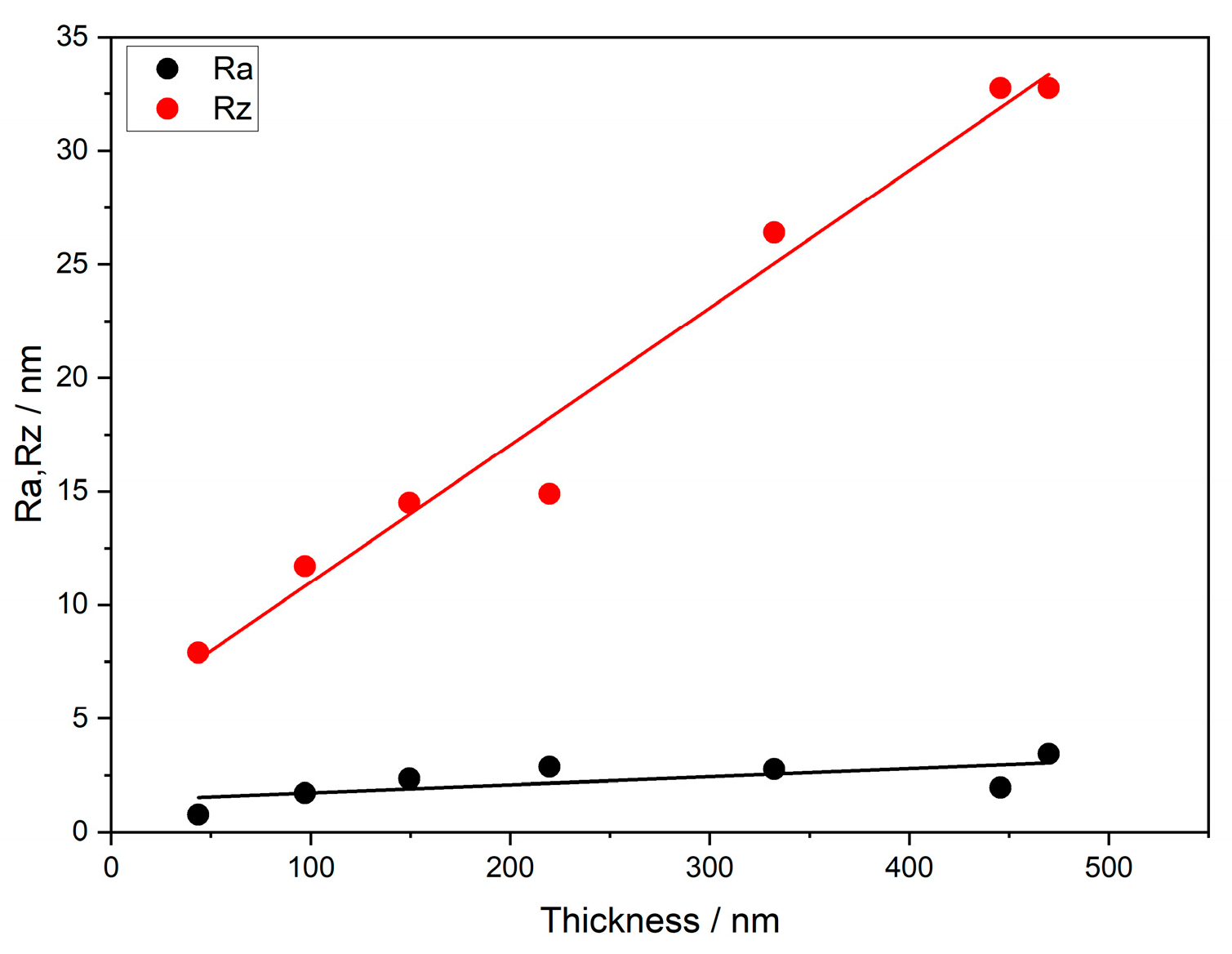
As shown in Figure 7, the dependence of the surface roughness parameters Ra (arithmetical mean roughness) and Rz (average maximum height of the profile) on the thickness of the deposited gold layers.
Figure 7. Ra and Rz parameters for different sample thicknesses.
Coatings 15 01240 g007
Both parameters exhibit an increasing trend with layer thickness; however, the intensity of this increase differs significantly. The Ra parameter rises moderately and almost linearly, suggesting a gradual increase in the mean roughness of the surface, with additional material deposition. In contrast, Rz demonstrates a pronounced and nearly linear growth, indicating a substantial enhancement of the peak-to-valley differences at higher thicknesses. This behavior can be attributed to the growth mechanism of gold grains on the substrate. As the thickness increases, the grain morphology tends to evolve toward columnar or pillar-like structures. Consequently, the valleys between grains become deeper, while the summits grow higher, producing larger surface irregularities. Since Rz is highly sensitive to extreme height variations, its response to thickness is stronger than that of Ra.
The increase in the roughness values of thin gold layers has a detrimental impact on their performance as electrical contacts. As surface roughness increases, the actual area of contact between the layers and opposing surfaces decreases, leading to a rise in contact resistance. This reduction in effective contact area results in poorer electrical conductivity and can cause localized current crowding, which further degrades the performance of the contact over time. In addition, high roughness may contribute to the formation of micro-gaps and discontinuities at the interface, making the contact less reliable, especially under mechanical or thermal stress. Therefore, maintaining low roughness in thin gold films is critical for ensuring stable and efficient electrical performance in electronic devices [33,34].

3.4. Conductivity

This section presents a comparison of the measured sheet resistance of gold films, with deposition parameters such as sputtering current, deposition time, and sample–target distance, as well as with the resulting film thickness. Since gold is widely used as a contact material in gas sensors and electronic devices due to its high conductivity and chemical inertness [41], maintaining low resistance is essential for reliable device performance. The resistivity of thin films is strongly affected by their thickness, microstructure, and continuity—all of which are influenced by the deposition conditions. The following results allow for an evaluation of how changes in process parameters affect the electrical quality of the films through their impact on thickness and structure.
Resistivity calculations are based on sheet-resistant measurements, performed by the four-point probe method (Equation (5)):
ρ = R S d
where ρ—resistivity [Ω/m], Rs—sheet resistance [Ω/sq], and d—layer thickness [nm].
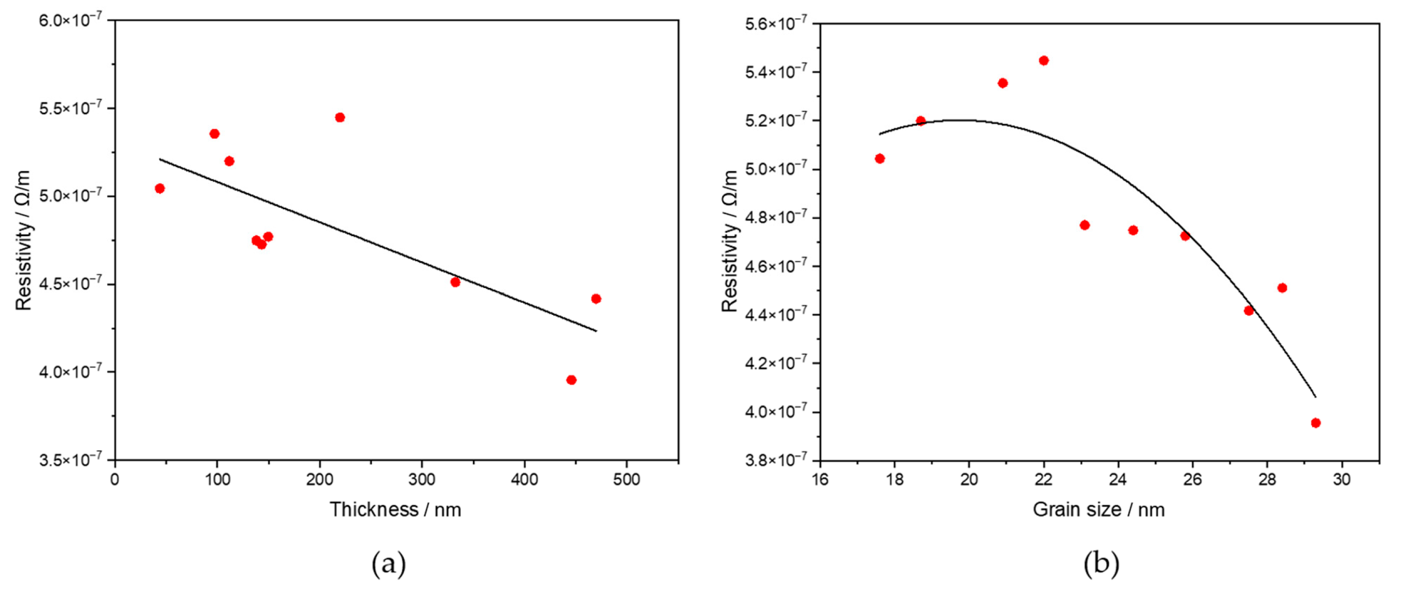
The influence of film thickness and grain size on the resistivity of sputtered gold layers is presented in Figure 8. As shown in Figure 8a, the resistivity decreases linearly with increasing film thickness, dropping from approximately 5.36 × 10⁻⁷ Ω/m for 43.7 nm to 3.96 × 10⁻⁷ Ω/m for 445.7 nm. This trend is consistent with classical size–effect models, where surface and interface scattering dominate in thin metallic films, leading to increased resistivity for thinner layers [42].
The non-monotonic behavior of resistivity to grain size in our gold films (see Figure 8b) can be understood in terms of competing scattering mechanisms. For grain sizes below approximately 22 nm, the resistivity increases with grain growth, as the disproportionately large grain-boundary area provides numerous scattering centers that impede the electron flow [43,44]. These grain boundaries, characterized by misoriented atomic lattices and excess volume, introduce potential barriers whose cumulative effect dominates transport in the ultrafine regime [45].
Once the average grain size surpasses a critical threshold—around 25 nm in our case—a pronounced drop in resistivity occurs, signaling a crossover to bulk-like conduction, where intragrain scattering prevails [46]. This critical scale corresponds closely to the electron mean free path in gold at room temperature (~35 nm), beyond which the contribution of grain-boundary scattering rapidly diminishes [46,47]. As grains grow larger, improved crystallinity and reduced defect densities further enhance electron mobility, driving resistivity toward the bulk value [47,48].
Even for grain sizes up to ~29 nm, a residual tail in the resistivity trend can persist due to scattering at low-angle boundaries and twin defects, which remain efficient reflectors of conduction electrons [45,49]. Similar size-dependent resistivity trends have been observed in other noble-metal thin films and nanowires, underlining the universality of grain-boundary and surface scattering effects in nanoscale conductors [50].
For applications in sensors and electrochemical electrodes, these findings highlight the necessity of tuning sputtering parameters to promote grain growth beyond the critical size. Achieving films with grains larger than ~25 nm ensures a low resistivity contact layer that closely approaches the intrinsic conductivity of bulk gold, thereby maximizing signal fidelity and minimizing spurious contact contributions [51].
To extend the electrical characterization, Hall effect measurements were conducted. The measurements were performed according to the Van Der Pauw method, using gold-coated contact probes placed right into the corners of the sample; this contact geometry ensures an ohmic response between probes.
To restrain the influence of surroundings on the readings, samples and probes were closed in a tight casing with nitrogen flow. All measurements were conducted in a 0.556 T magnetic field, with 20 mA of testing current, and a temperature of 300 K. In all analyzed cases, because of the metal properties of analyzed samples, the charge carriers refer to electrons.
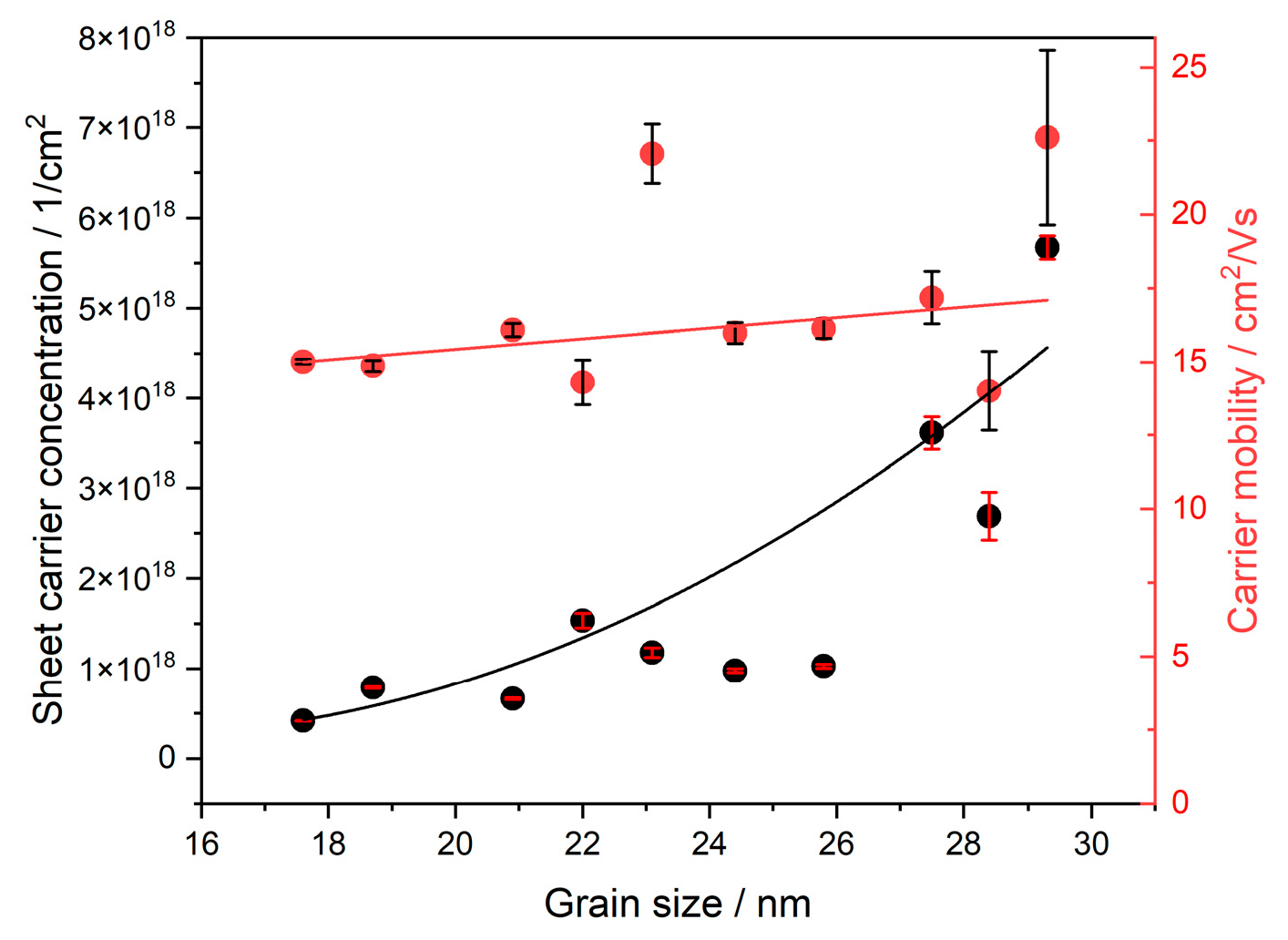
As observed in Figure 9, both the sheet carrier concentration (SCC) and carrier mobility (CM) increase with grain size, consistent with the concurrent decrease in electrical resistivity. The SCC exhibits a near-exponential dependence on the average grain size of gold, increasing from 4.2 × 1017 cm−2, for a sample with an average grain size of 17.6 nm, to 5.7 × 1018 cm−2, for a sample with an average grain size of 29.3 nm. This behavior can be attributed to a reduction in defect density, resulting from the decreased fraction of grain boundaries. Such boundaries often host electron traps, lattice distortions, and other structural imperfections that either localize or scatter charge carriers, thereby lowering the effective SCC. The reduction in the grain-boundary area consequently mitigates carrier trapping and scattering, leading to an overall increase in the measured SCC. The CM also increases with grain size, but much more slowly than SCC. This phenomenon may be caused by the increased electron mean free path, due to fewer grain boundaries (potential barriers) along their paths. The slower increase in the CM compared to the SCC can be explained by the higher density of free electrons in the bulk material (caused by grain size growth), which enhances carrier collisions and leads to a lower-mean free path (and thus lower mobility).
To validate the reliability of the electrical parameters obtained, our results were compared with reported data for sputtered gold thin films. Similar quantitative relationships between the microstructure and electrical properties of sputtered gold films have been reported in previous studies. Slepička et al. found that increasing the film thickness from approximately 5 nm to 80 nm reduced the resistivity from about 5 × 10⁻⁷ Ω·m to 3 × 10⁻⁷ Ω·m, as isolated islands coalesced into a continuous metallic layer, enhancing electron transport [9]. Robles et al. reported resistivity values between 2.8 × 10⁻⁷ and 4.9 × 10⁻⁷ Ω·m for Au films on mica. Samples with smaller grains and higher surface roughness were characterized by the highest resistivity because of the intensive grain-boundary scattering [44]. Siegel et al. observed comparable values (≈3.0–5.2 × 10⁻⁷ Ω·m) for sputtered Au on glass, emphasizing that improved continuity and structural ordering markedly lowered the sheet resistance [52]. Zhang et al. further demonstrated that when the grain size exceeded ~25 nm, resistivity approached bulk-like values (≈2.5 × 10⁻⁷ Ω·m), with carrier concentrations in the 1018–1019 cm−3 range and mobilities up to 60 cm2 V−1 s−1 [51]. Likewise, Libanský et al. reported resistivity values around 4 × 10⁻⁷ Ω·m for 100 nm Au films on glass, consistent with those obtained in the present study [14].
Overall, these numerical comparisons confirm that the resistivity (≈3–5 × 10⁻⁷ Ω·m), carrier concentration (1017–1019 cm−3), and mobility (20–60 cm2 V−1 s−1) measured in this work fall squarely within the range reported for magnetron-sputtered gold thin films, validating the reliability of the electrical performance achieved under the optimized deposition conditions.
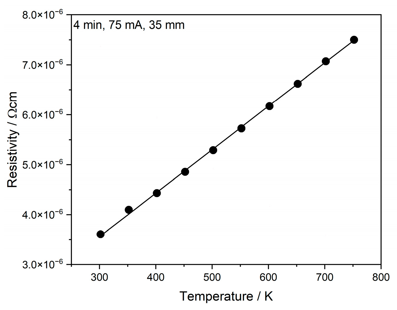
To further investigate gold layers for use in sensor technologies or electrochemical applications, high-temperature Hall effect measurements were conducted, as these applications typically require the use of high temperatures. As mentioned earlier, for our tests, a temperature range of 300 K to 750 K was chosen to ensure that observed changes depended only on temperature, and the measurement chamber was constantly flushed with nitrogen to exclude potential oxidation of samples or probes from result analysis.
As observed in Figure 10, the resistivity increases linearly with temperature, indicating that in the tested temperature range (300–750 K), processes such as thermal relaxation, recrystallization, or grain-merging did not occur. Because of its manner and very low-value change in gold resistance, it should not have had any influence on the device.
The next step was to investigate SCC and CM behavior at various temperatures.
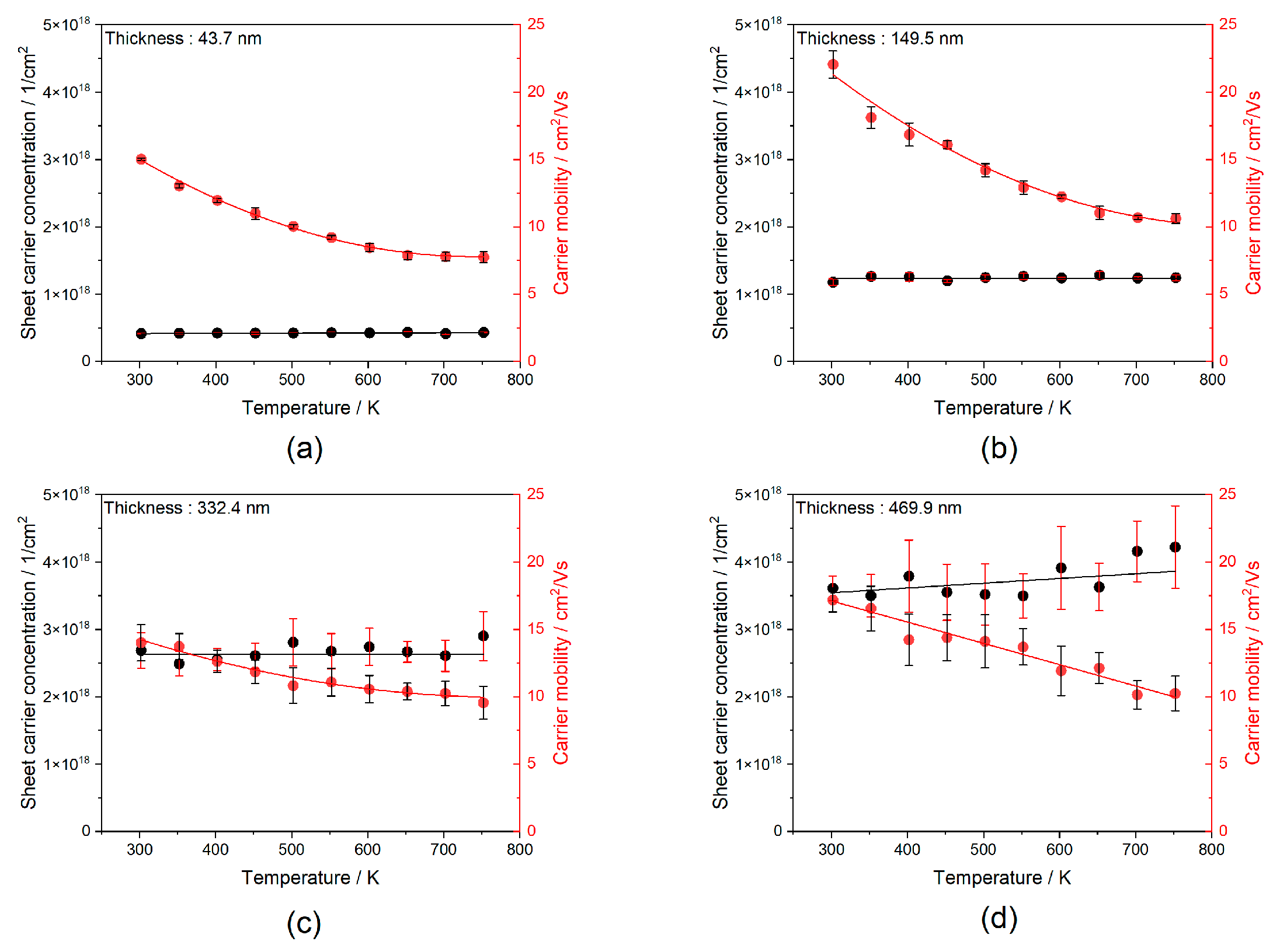
As shown in Figure 11, the sheet carrier concentration in gold thin films with thicknesses of 43.7 nm, 149.5 nm, and 332.4 nm remains nearly constant over the investigated temperature range of 300–750 K. In contrast, the thickest film (469.9 nm) exhibits a slight increase in SCC with a rising temperature. Carrier mobility decreases systematically with temperature for all samples, which can be attributed to enhanced carrier-scattering by phonons at elevated temperatures. The increase in SCC observed for the thickest film may be related to the reduced influence of surface and interface scattering, improved crystalline continuity, and possible thermally induced activation of additional conduction channels within the bulk of the film. These trends are consistent with electron transport in polycrystalline gold, where thinner films are dominated by surface and grain-boundary effects, while thicker films behave more like bulk metal.
Comparable temperature-dependent electrical behavior has been reported for sputtered gold thin films by several authors. Bendavid et al. [53] observed a nearly linear increase in resistivity with temperature for RF-sputtered Au films, confirming that phonon scattering is the dominant mechanism that is limiting carrier mobility at elevated temperatures. Siegel et al. [32] reported that sputtered Au films on glass exhibited sheet resistances in the range of 3.0–5.2 × 10⁻⁷ Ω·m, with only slight changes in resistivity between 300 K and 700 K, indicating stable carrier concentration and phonon-limited conduction. In turn, Martin et al. [54] demonstrated that obliquely sputtered gold films maintain metallic conduction behavior, showing a moderate resistivity increase from ~3.8 × 10⁻⁷ Ω·m at 300 K to ~4.5 × 10⁻⁷ Ω·m at 600 K, in accordance with phonon scattering in consolidated grains. These studies confirm that while carrier concentration in gold films remains almost constant with temperature, carrier mobility systematically decreases due to enhanced electron–phonon interactions. Thinner films, which are more affected by grain-boundary and surface scattering, demonstrate higher resistivity and a stronger temperature dependence, compared to thicker layers that behave more like bulk metal. The present results, i.e., nearly constant SCC and a gradual mobility reduction between 300 K and 750 K, with a minor SCC increase for the thickest film, are therefore fully consistent with the established metallic transport behavior of sputtered polycrystalline gold. Therefore, the electrical stability observed at up to 750 K confirms the robustness of the films for high-temperature sensor applications.
From an electrical transport perspective, the observed reduction in carrier mobility is the dominant factor governing the temperature dependence of the film resistance. Since the SCC remains nearly constant for most thicknesses, the increase in resistivity with temperature is primarily attributed to mobility degradation, due to enhanced phonon scattering. This behavior aligns with the classical metallic conduction model, in which temperature-induced lattice vibrations increase electron scattering rates, leading to a proportional rise in electrical resistance [42].
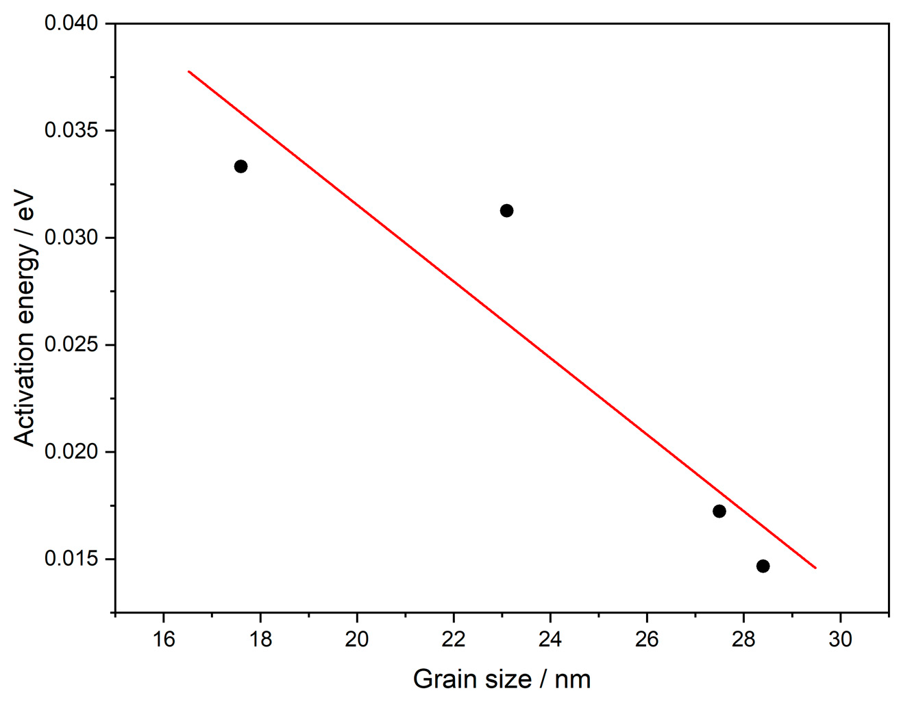
To verify the claim regarding grain boundaries’ influence on the electronic properties of material, based on varied temperature and Hall effect measurements, Arrhenius plots were made and activation energy (Ea) [55] was calculated for few samples with different grain sizes, and presented in Figure 12.
As expected for high-conductivity material like gold, in general, Ea for all tested samples is low; however, there is a very visible trend when Ea decreases with grain size value: from 0.033 eV for the sample with 17.6 nm mean grain size to 0.015 eV for the sample with 28.4 nm mean grain size. Taking into account that bigger grains implicate less grain boundaries, this trend proved that grain boundaries have an actual impact on charge transport in thin gold layers.

4. Conclusions

The present study demonstrates that DC magnetron sputtering offers precise control over the morphology, crystallinity, and electrical properties of gold thin films for electrochemical and sensor applications. By systematically varying sputtering current, deposition time, and target–substrate distance under a constant Ar pressure, we achieved tunable film thicknesses (44–470 nm), with a predominantly (111) FCC texture. Post-deposition WDXRF confirmed excellent thickness reproducibility, while AFM and XRD analyses revealed that increasing film thickness promotes grain coarsening and higher surface roughness, accompanied by subtle peak asymmetries and angular shifts that are indicative of evolving strain and transient defects.
Electrical measurements showed that sheet resistivity scales inversely with thickness, and exhibits a critical grain-size threshold near 25 nm: below this value, grain-boundary scattering dominates, raising resistivity, whereas above it, intragrain transport prevails, driving resistivity sharply downward toward bulk gold values.
High-temperature Hall effect analysis showed that the increase in resistance at higher temperatures was accompanied by a corresponding decrease in carrier mobility.
Together, these findings highlight the interplay between deposition parameters and film microstructure, providing clear guidelines for fabricating gold electrodes with optimized conductivity and structural integrity. Future work will explore in situ substrate heating and alloying strategies to further tailor film properties, aiming to enhance performance in demanding electrochemical and resistive-sensor environments.

Supplementary Materials

The following supporting information can be downloaded at: https://www.mdpi.com/article/10.3390/coatings15111240/s1, Figure S1. EDS spectrum of the gold sample. Figure S2. Influence of (a) deposition time, (b) applied current, and (c) target-substrate distance on Cu-Kα spectra. Figure S3. Intensity- (a) current, (b) time, and (c) distance dependencies for deposited thin films. Figure S4. XRD diffraction patterns for scan range from 33 to 44o. Table S1. Crystalline grain size depending on synthesis parameters. (See Refs. [27,56,57,58,59]).

Author Contributions

Conceptualization, W.B. and K.S.; methodology, W.B., K.S., P.Ż., and M.W.; validation, W.B., and K.S.; formal analysis, P.Ż.; investigation, W.B., K.S., P.Ż., and M.W.; resources, W.B.; data curation, W.B.; writing—original draft preparation, W.B., and K.S.; writing—review and editing, M.W.; visualization, W.B., and K.S.; supervision, M.W.; project administration, W.B.; funding acquisition, M.W. and. W.B. All authors have read and agreed to the published version of the manuscript.

Funding

Grant of Initiative for Excellence—Research University of AGH University of Krakow, grant IDUB no. 12509.

Institutional Review Board Statement

Not applicable.

Informed Consent Statement

Not applicable.

Data Availability Statement

Data set available from the authors on request.

Conflicts of Interest

The authors declare no conflicts of interest.

References

  1. Burke, L.D. Scope for new applications for gold arising from the electrocatalytic behaviour of its metastable surface states. Gold Bull. 2004, 37, 125–135. [Google Scholar] [CrossRef]
  2. Déronzier, T.; Morfin, F.; Massin, L.; Lomello, M.; Rousset, J.L. Pure nanoporous gold powder: Synthesis and catalytic properties. Chem. Mater. 2011, 23, 5287–5289. [Google Scholar] [CrossRef]
  3. Mortari, A.; Maaroof, A.; Martin, D.; Cortie, M.B. Mesoporous gold electrodes for sensors based on electrochemical double layer capacitance. Sens. Actuators B Chem. 2007, 123, 262–268. [Google Scholar] [CrossRef]
  4. Kvítek, O.; Kopáček, V.; Švorčík, V. Gold nanostructures in gas chemical sensor technology. Chem. Listy 2018, 112, 175–182. [Google Scholar]
  5. Bulowski, W.; Knura, R.; Socha, R.P.; Basiura, M.; Skibińska, K.; Wojnicki, M. Thin Film Semiconductor Metal Oxide Oxygen Sensors: Limitations, Challenges, and Future Progress. Electronics 2024, 13, 3409. [Google Scholar] [CrossRef]
  6. Bulowski, W.; Socha, R.P.; Drabczyk, A.; Kasza, P.; Panek, P.; Wojnicki, M. Molecular Layer Doping ZnO Films as a Novel Approach to Resistive Oxygen Sensors. Electronics 2025, 14, 595. [Google Scholar] [CrossRef]
  7. Dong, L.; Wu, X.; Hu, Y.; Xu, X.; Bao, H. Suppressed Thermal Conductivity in Polycrystalline Gold Nanofilm: The Effect of Grain Boundary and Substrate. Chin. Phys. Lett. 2021, 38, 027202. [Google Scholar] [CrossRef]
  8. Ali, Z.I.; Radwan, S.I.; Shehata, M.M.; Ghazy, O.A.; Saleh, H.H. Structural, optical and electrical properties of PVC/Au thin films prepared by sputtering process. Opt. Quantum Electron. 2021, 53, 241. [Google Scholar] [CrossRef]
  9. Slepička, P.; Kolská, Z.; Náhlík, J.; Hnatowicz, V.; Švořcík, V. Properties of Au nanolayers on polyethyleneterephthalate and polytetrafluoroethylene. Surf. Interface Anal. 2009, 41, 741–745. [Google Scholar] [CrossRef]
  10. Radwan, S.I.; Rashad, A.M.; Tantawy, H.R.; Samad, S.A. Effect of Annealing and Ion Beam Irradiation on AC Electrical Properties for Gold Sputtered PM-355. Indian J. Pure Appl. Phys. 2022, 60, 171–181. [Google Scholar] [CrossRef]
  11. Švorčík, V.; Kvítek, O.; Lyutakov, O.; Siegel, J.; Kolská, Z. Annealing of sputtered gold nano-structures. Appl. Phys. A 2011, 102, 747–751. [Google Scholar] [CrossRef]
  12. Švorčík, V.; Siegel, J.; Sutta, P.; Mistrík, J.; Janicek, P.; Worsch, P.; Kolská, Z. Annealing of gold nanostructures sputtered on glass substrate. Appl. Phys. A 2011, 102, 605–610. [Google Scholar] [CrossRef]
  13. Chen, J.-Q.; Huang, Q.-S.; Qi, R.-Z.; Feng, Y.-F.; Feng, J.-T.; Zhang, Z.; Li, W.-B.; Wang, Z.-S. Effects of sputtering power and annealing temperature on surface roughness of gold films for high-reflectivity synchrotron radiation mirrors. Nucl. Sci. Tech. 2019, 30, 107. [Google Scholar] [CrossRef]
  14. Libansky, M.; Zima, J.; Barek, J.; Reznickova, A.; Svorcik, V.; Dejmkova, H. Basic electrochemical properties of sputtered gold film electrodes. Electrochim. Acta 2017, 251, 452–460. [Google Scholar] [CrossRef]
  15. Casuse, T.Q.; Benavidez, A.; Plumley, J.B.; Tsui, L.-K.; Ali, A.-M.; Cerrato, J.M.; Garzon, F.H. DC Sputtered Ultralow Loading Gold Nanofilm Electrodes for Detection of As (III) in Water. ECS Sens. Plus 2022, 1, 014602. [Google Scholar] [CrossRef]
  16. Yang, B.; Wang, C.; Xiao, R.; Yu, H.; Wang, J.; Liu, H.; Xia, F.; Xiao, J. High sensitivity and fast response sensor based on sputtering Au tuned ZnFe2O4-SE for low concentration NH3 detection. Mater. Chem. Phys. 2020, 239, 122302. [Google Scholar] [CrossRef]
  17. Sun, Z.; Lü, J.; Song, X. Microstructure and electrical properties of ultrathin gold films prepared by DC sputtering. Vacuum 2010, 85, 297–301. [Google Scholar] [CrossRef]
  18. Markert, C.; Lützenkirchen-Hecht, D.; Frahm, R. Structural and electrical properties of thin d.c. magnetron-sputtered gold films deposited on float glass. Surf. Interface Anal. 2006, 38, 715–718. [Google Scholar] [CrossRef]
  19. Zhang, X.; Song, X.-H.; Zhang, D.-L. Thickness dependence of grain size and surface roughness for dc magnetron sputtered Au films. Chin. Phys. B 2010, 19, 086802. [Google Scholar] [CrossRef]
  20. Li, B.; Huang, L.; Zhou, M.; Fan, X.; Ma, M. Preparation and spectral analysis of gold nanoparticles using magnetron sputtering and thermal annealing. J. Wuhan Univ. Technol.-Mater. Sci. Ed. 2014, 29, 651–655. [Google Scholar] [CrossRef]
  21. Persson, A.; Bergström, J.; Burman, C.; Hogmark, S. Influence of deposition temperature and time during PVD coating of CrN on corrosive wear in liquid aluminium. Surf. Coat. Technol. 2001, 146-147, 42–47. [Google Scholar] [CrossRef]
  22. Thaveedeetrakul, A.; Witit-anun, N.; Boonamnuayvitaya, V. The role of target-to-substrate distance on the DC magnetron sputtered zirconia thin films’ bioactivity. Appl. Surf. Sci. 2012, 258, 2612–2619. [Google Scholar] [CrossRef]
  23. Wuhrer, R.; Yeung, W.Y. Effect of target–substrate working distance on magnetron sputter deposition of nanostructured titanium aluminium nitride coatings. Scr. Mater. 2003, 49, 199–205. [Google Scholar] [CrossRef]
  24. Li, J.; An, Q.; Fang, H. Monte Carlo simulation of deposition uniformity in the triple-target magnetron co-sputtering system. Appl. Surf. Sci. 2024, 646, 158914. [Google Scholar] [CrossRef]
  25. Syed, M.; Glaser, C.; Syed, M. Surface Morphology of Gold Thin Films using RF Magnetron Sputtering. In Proceedings of the 60th Annual Technical Conference, SVC TechCon, Providence, RI, USA, 29 April–4 May 2017. [Google Scholar] [CrossRef]
  26. Kejzlar, J.; More-Chevalier, J.; Hruška, M.; Otta, J.; Fitl, P.; Novotný, M.; Poupon, M.; Hruška, P.; Prokop, D.; Cichoň, S.; et al. Black gold layers: Preparation via thermal evaporation, material and optical properties, and application potential for gas sensors. Mater. Adv. 2025, 6, 3280–3292. [Google Scholar] [CrossRef]
  27. Mech, K.; Kowalik, R.; Żabiński, P. Cu Thin Films Deposited by DC Magnetron Sputtering for Contact Surfaces on Electronic Components. Arch. Metall. Mater. 2011, 56, 903–908. [Google Scholar] [CrossRef]
  28. Haynes, W.M. CRC Handbook of Chemistry and Physics; CRC Press: Boca Raton, FL, USA, 2016. [Google Scholar]
  29. Rossnagel, S.M. Sputter deposition for semiconductor manufacturing. IBM J. Res. Dev. 1999, 43, 163–179. [Google Scholar] [CrossRef]
  30. Westwood, W.D. Sputter Deposition; AVS: New York, NY, USA, 2003. [Google Scholar]
  31. Sitko, R. Quantitative X-ray fluorescence analysis of samples of less than ‘infinite thickness’: Difficulties and possibilities. Spectrochim. Acta Part B At. Spectrosc. 2009, 64, 1161–1172. [Google Scholar] [CrossRef]
  32. Mezher, S.; Dawood, M.; Kadhim, D.B. Optical Observations of Sputtered Au-nanostructures and Characterizations. J. Tech. 2024, 6, 93–102. [Google Scholar] [CrossRef]
  33. Rai, V.; Srivastava, A. Correlation Between Optical and Morphological Properties of Nanostructured Gold Thin Film. JSM Nanotechnol. Nanomed. 2016, 4, 1039. [Google Scholar]
  34. Dupré, L.; Buttard, D.; Leclere, C.; Renevier, H.; Gentile, P. Gold contamination in VLS-grown Si nanowires: Multiwavelength anomalous diffraction investigations. Chem. Mater. 2012, 24, 4511–4516. [Google Scholar] [CrossRef]
  35. Viter, R.; Balevicius, Z.; Abou Chaaya, A.; Baleviciute, I.; Tumenas, S.; Mikoliunaite, L.; Ramanavicius, A.; Gertnere, Z.; Zalesska, A.; Vataman, V.; et al. The influence of localized plasmons on the optical properties of Au/ZnO nanostructures. J. Mater. Chem. C 2015, 3, 6815–6821. [Google Scholar] [CrossRef]
  36. Pandey, S.C.; Sharma, S.; Pandey, K.K.; Gupta, P.; Rai, S.; Singh, R.; Chattopadhyay, M.K. Sputtering current driven growth and transport characteristics of superconducting Ti40V60 alloy thin films. J. Appl. Phys. 2025, 137, 113902. [Google Scholar] [CrossRef]
  37. Al-Allaq, A.H.; Tabassum, N.; Mohammed, Y.S.; Elmustafa, A.A. Sputtering-driven microstructure and mechanical behavior in NbMoTaW high-entropy alloy films. Mater. Chem. Phys. 2025, 340, 130694. [Google Scholar] [CrossRef]
  38. Alvarez, R.; Garcia-Valenzuela, A.; Regodon, G.; Ferrer, F.J.; Rico, V.; Garcia-Martin, J.M.; Gonzalez-Elipe, A.R.; Palmero, A. Growth dynamics of nanocolumnar thin films deposited by magnetron sputtering at oblique angles. Nanotechnology 2024, 35, 095705. [Google Scholar] [CrossRef]
  39. Malinský, P.; Slepička, P.; Hnatowicz, V.; Svorčík, V. Early stages of growth of gold layers sputter deposited on glass and silicon substrates. Nanoscale Res. Lett. 2012, 7, 241. [Google Scholar] [CrossRef]
  40. Barreca, D.; Gasparotto, A.; Pierangelo, E.; Tondello, E. Nucleation and growth of gold nanoparticles deposited by RF-sputtering: An experimental study. MRS Online Proc. Libr. 2004, 818, 227–232. [Google Scholar] [CrossRef]
  41. Milone, A.; Monteduro, A.G.; Rizzato, S.; Leo, A.; Di Natale, C.; Kim, S.S.; Maruccio, G. Advances in Materials and Technologies for Gas Sensing from Environmental and Food Monitoring to Breath Analysis. Adv. Sustain. Syst. 2023, 7, 2200083. [Google Scholar] [CrossRef]
  42. Fuchs, K. The conductivity of thin metallic films according to the electron theory of metals. Math. Proc. Camb. Philos. Soc. 1938, 34, 100–108. [Google Scholar] [CrossRef]
  43. Bishara, H.; Ghidelli, M.; Dehm, G. Approaches to Measure the Resistivity of Grain Boundaries in Metals with High Sensitivity and Spatial Resolution: A Case Study Employing Cu. ACS Appl. Electron. Mater. 2020, 2, 2049–2056. [Google Scholar] [CrossRef]
  44. Robles, M.E.; Gonzalez-Fuentes, C.A.; Henriquez, R.; Kremer, G.; Moraga, L.; Oyarzun, S.; Suarez, M.A.; Flores, M.; Munoz, R.C. Resistivity of thin gold films on mica induced by electron–surface scattering: Application of quantitative scanning tunneling microscopy. Appl. Surf. Sci. 2012, 258, 3393–3404. [Google Scholar] [CrossRef]
  45. Bishara, H.; Lee, S.; Brink, T.; Ghidelli, M.; Dehm, G. Understanding Grain Boundary Electrical Resistivity in Cu: The Effect of Boundary Structure. ACS Nano 2021, 15, 16607–16615. [Google Scholar] [CrossRef]
  46. Kästle, G.; Boyen, H.G.; Schröder, A.; Plettl, A.; Ziemann, P. Size effect of the resistivity of thin epitaxial gold films. Phys. Rev. B 2004, 70, 165414. [Google Scholar] [CrossRef]
  47. Durkan, C.; Welland, M.E. Size effects in the electrical resistivity of polycrystalline nanowires. Phys. Rev. B 2000, 61, 14215–14218. [Google Scholar] [CrossRef]
  48. Zhang, Q.G.; Zhang, X.; Cao, B.Y.; Fujii, M.; Takahashi, K.; Ikuta, T. Influence of grain boundary scattering on the electrical properties of platinum nanofilms. Appl. Phys. Lett. 2006, 89, 114102. [Google Scholar] [CrossRef]
  49. Feldman, B.; Park, S.; Haverty, M.; Shankar, S.; Dunham, S.T. Simulation of grain boundary effects on electronic transport in metals, and detailed causes of scattering. Phys. Status Solidi B 2010, 247, 1791–1796. [Google Scholar] [CrossRef]
  50. Moors, K.; Sorée, B.; Magnus, W. Resistivity scaling in metallic thin films and nanowires due to grain boundary and surface roughness scattering. Microelectron. Eng. 2017, 167, 37–41. [Google Scholar] [CrossRef]
  51. Zhang, X.; Song, X.; Zhang, X.-G.; Zhang, D. Grain boundary resistivities of polycrystalline Au films. Europhys. Lett. 2011, 96, 17010. [Google Scholar] [CrossRef]
  52. Siegel, J.; Lyutakov, O.; Rybka, V.; Kolská, Z.; Svorčík, V. Properties of gold nanostructures sputtered on glass. Nanoscale Res. Lett. 2011, 6, 96. [Google Scholar] [CrossRef]
  53. Bendavid, A.; Martin, P.J.; Wieczorek, L. Morphology and optical properties of gold thin films prepared by filtered arc deposition. Thin Solid Film. 1999, 354, 169–175. [Google Scholar] [CrossRef]
  54. Martin, N.; Martin, E.; Cote, J.-M.; Sthal, F.; Gavoille, J.; Raschetti, M.; Oliveri, S. Low temperature dependence of resistivity in obliquely sputter-deposited gold thin films. Surf. Coat. Technol. 2025, 499, 131884. [Google Scholar] [CrossRef]
  55. Streletskiy, O.A.; Zavidovskiy, I.A.; Nischak, O.Y.; Dvoryak, S.V. Electrical conductivity and structural properties of a-C:N films deposited by ion-assisted pulse-arc sputtering. Thin Solid Film. 2020, 701, 137948. [Google Scholar] [CrossRef]
  56. Spiridonov, J. Limits Of Measurement of Thickness and Elemental Composition with a Portable Xrf Analyzer. Univers. Tech. Sci. 2021, 5, 86. [Google Scholar] [CrossRef]
  57. Vogt, C.; Dargel, R. Determination of layer thickness with μXRF. Appl. Surf. Sci. 2005, 252, 53–56. [Google Scholar] [CrossRef]
  58. Giurlani, W.; Berretti, E.; Innocenti, M.; Lavacchi, A. Coating Thickness Determination Using X-ray Fluorescence Spectroscopy: Monte Carlo Simulations as an Alternative to the Use of Standards. Coatings 2019, 9, 79. [Google Scholar] [CrossRef]
  59. Porcinai, S.; Ferretti, M. X-ray fluorescence-based methods to measure the thickness of protective organic coatings on ancient silver artefacts. Spectrochim. Acta Part B At. Spectrosc. 2018, 149, 184–189. [Google Scholar] [CrossRef]
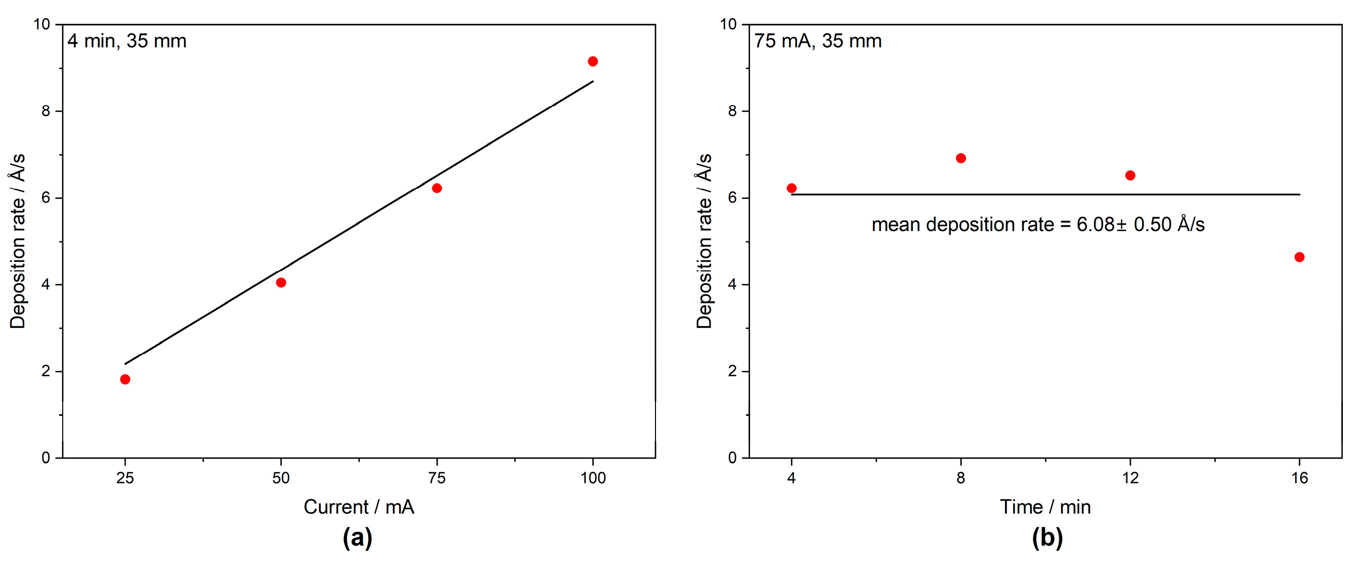
Figure 1. Deposition rates for different sputtering currents (a) and different sputter times (b).
Coatings 15 01240 g001
Figure 2. UV-Vis spectra of selected samples (a) and correlation between thickness and absorbance (b).
Coatings 15 01240 g002
Figure 3. XRD pattern of Au thin film.
Coatings 15 01240 g003
Figure 4. Dependence between the thickness and grain size.
Coatings 15 01240 g004
Figure 5. Microstrains in samples obtained with different deposition currents.
Coatings 15 01240 g005
Figure 8. Resistivity of thin gold film, depending on layer thickness (a) and grain size (b).
Coatings 15 01240 g008
Figure 9. Electrical parameters of gold samples, according to their grain size.
Coatings 15 01240 g009
Figure 10. Resistivity of sputtered gold sample at elevated temperatures.
Coatings 15 01240 g010
Figure 11. Electrical parameters in the temperature range of 300–750 K of samples with thicknesses of 43.7 nm (a), 149.5 nm (b), 332.4 nm (c), and 469.9 nm (d).
Coatings 15 01240 g011
Figure 12. Activation energy for samples with different grain sizes.
Coatings 15 01240 g012
Table 1. Results of spectrum analysis.
Element
Number
Element
Symbol
Element
Name
Atomic
Conc.
Weight
Conc.
79AuGold95.00%99.68%
6CCarbon5.00%0.32%
Table 2. Results of thickness calculations.
Current/mADistance/mmTime/minSubstrate Weight/gSubstrate Weight with Au/gAu Weight/gThickness/nm
253542.094802.095560.0007643.7
503542.089712.091400.0016997.2
753542.095782.098380.00260149.5
1003542.097532.101350.00382219.7
753582.094542.100320.00578332.4
7535122.095382.103550.00817469.9
7535162.095122.102870.00775445.7
753342.100472.102410.00194111.6
753142.100632.103120.00249143.2
752942.097972.100370.00240138.0
Table 3. Microstrains from W–H analysis for samples with different thickness.
Sample Thickness [nm]Microstrains from W–H Analysis
43.70.01094
97.20.00208
149.5−0.01261
219.70.00827
Disclaimer/Publisher’s Note: The statements, opinions and data contained in all publications are solely those of the individual author(s) and contributor(s) and not of MDPI and/or the editor(s). MDPI and/or the editor(s) disclaim responsibility for any injury to people or property resulting from any ideas, methods, instructions or products referred to in the content.