Abstract
Cu2S has wide-ranging applications in the energy field, particularly as electrode materials and components of energy storage devices. However, the migration of copper ions is prone to component segregation and copper precipitation, impairing long-term thermal stability and service performance. Ce2S3 not only possesses the unique 4f electron layer structure of Ce but also has high thermal stability and chemical inertness. Here, we report for the first time that the thermal stability and mechanical properties of Cu2S can be significantly enhanced by introducing the dispersed phase Ce2S3. Thermogravimetry—differential scanning calorimetry (TG-DSC) results show that the addition of 6 wt% Ce2S3 improves the thermal stability of Cu2S sintered at 400 °C. X-ray diffraction (XRD) results indicate that the crystal structure of Cu2S gradually transforms to tetragonal Cu1.96S and orthorhombic Cu1.8S phase at 400 °C with the increase of Ce2S3 addition. Scanning electron microscopy (SEM) results show that the particle size gradually decreased with the increase of Ce2S3 amount, indicating that the Ce2S3 addition increased the reactivity. The Ce content in Cu2S increased gradually with the increase of Ce2S3 amount at 400–600 °C. The 7 wt% Ce2S3-Cu2S exhibits paramagnetic behavior with a saturation magnetization of 1.2 µB/Ce. UV-Vis analysis indicates that the addition of Ce2S3 can reduce the optical energy gap and enrich the band structure of Cu2S. With increasing addition of Ce2S3 and rising sintering temperature, the density of Ce2S3-Cu2S gradually increases, and the hardness of Ce2S3-Cu2S increases by 52.5% at 400 °C and by 34.2% at 600 °C. The friction test results show that an appropriate addition amount of Ce2S3 can increase the friction coefficients of Cu2S. Ce2S3 modification offers a novel strategy to simultaneously enhance the structural and service stability of Cu2S by regulating Cu ion diffusion and suppressing compositional fluctuations.
1. Introduction
Multifunctional copper sulfide (Cu2S) exhibits broad interdisciplinary development prospects in the fields of solar cells [1] and photocatalytic degradation of pollutants [2], efficient ozone decomposition [3], and energy storage [4]. Cu2S exhibits a monoclinic structure at low temperature and transforms into a hexagonal structure at elevated temperatures, where copper ions behave in a quasi-liquid state, leading to intrinsically low lattice thermal conductivity [5]. Non-stoichiometric Cu2−xS (0 ≤ x ≤ 1) includes Cu1.96S, Cu1.8S and other forms [6,7,8]. By designing low-dimensional crystal structures, adjusting compositions, introducing elemental doping (Sn [5], Mn [9], Ag [10], Bi [11], Ni [12]), and constructing composites (CuO [13]), its electronic transport properties can be tuned, enabling outstanding performance.
Cu2S has been widely applied in energy-related fields such as energy storage devices and electrode materials; however, its poor thermal stability and mechanical properties limit its efficiency. The quasi-liquid migration of copper ions can enhance energy conversion efficiency, but the continuous migration often leads to compositional segregation and copper precipitation, thereby compromising device lifetime. The thermal stability of Cu2S can be enhanced through either elemental doping or composite formation, both of which suppress sulfur volatilization and oxidation at high temperatures. These approaches work synergistically, with doping reducing atomic-scale sulfur vacancy formation while composite matrices provide macroscopic diffusion barriers, simultaneously improving electrical and mechanical properties. The introduction of foreign atoms (Sn [5], Mn [9], Ag [10], Bi [11], Ni [12]) is a common method to hinder the migration of Cu ions and improve their stability. The limitations of elemental doping primarily involve lattice distortion and phase segregation induced by excessive dopant concentrations, along with thermally driven ion segregation (e.g., Zn2+) [14] that may create localized defects. Furthermore, certain high-valency dopants (e.g., Fe3+) [15] can introduce detrimental charge compensation effects that compromise material stability. The introduction of dispersed SiO2 [16] into Cu1.8S, 2% In2S3 [17], 1 wt% WSe2 into Cu1.8S [18], 1 wt% SiC into Cu1.8S [19] etc. plays an important role in synergistic improvement of material stability. The nanoscale second phase acts as effective ‘pinning centers’ in the Cu2S matrix, inhibiting both short-range Cu ion migration and long-range precipitation through constrained diffusion pathways, thereby significantly improving component stability. The drawbacks of compound hybridization include weak interfacial bonding in ex situ composites (e.g., van der Waals-dominated Cu2S/graphene interfaces) [20]. This paper has embarked on a quest for dopant materials that can simultaneously achieve elemental doping and sulfur vacancy passivation, thereby synergistically enhancing the thermal stability of Cu2S.
Ce2S3 uniquely combines the localized 4f-electron configuration characteristic of rare-earth elements [21] with superior optoelectronic properties and the structural advantages of sulfides. Ce demonstrates unique quantum modulation and energy band convergence effects [22]. Ce2S3 has a rich energy level structure, and good stability that makes it promising for improving the stability of Cu2S through dispersed doping. This dual-functional material Ce2S3 enables performance optimization of Cu2S through two synergistic approaches: (i) controlled cationic substitution (e.g., Ce3+→Cu+ doping to modify defect chemistry) and (ii) hybrid interface engineering (e.g., constructing charge-transfer-enabled Ce2S3/Cu2S heterojunctions). Ce2S3 modification not only enables band structure tuning and optical response enhancement through Ce-4f/Cu-3d orbital coupling but also introduces potential magnetic interactions via variable valence and 4f electrons, thereby opening pathways toward multifunctional Cu2S with coupled optical, magnetic, and transport properties.
Therefore, Cu2S powder was compounded with different Ce2S3 contents and was sintered under different sintering temperatures. Ce2S3 modification represents a rational strategy that integrates structural stabilization with ionic transport regulation. Such an approach not only addresses the intrinsic thermal and mechanical limitations of Cu2S but also provides new insights into designing sulfide-based functional materials with enhanced stability and efficiency for energy applications.
2. Experimental Sections
2.1. Preparation of the Ce2S3-Doped Cu2S
Initially, Cu2S powders (99% purity, Guangdong Yuanfeng Chemical Reagent Co., Ltd., Guangzhou, China) were weighed along with Ce2S3 addition of 0.25 wt%, 0.5 wt%, 0.75 wt%, 1 wt%, 3 wt%, 4 wt%, 5 wt%, 6 wt%, and 7 wt%. The mixture powders (about 1.5 g) were thoroughly ground and mixed uniformly. The evenly mixed reagent was cold pressed under the pressure of 5 MPa. Subsequently, the cold-pressed Ce2S3-doped Cu2S compacts (15 mm diameter) were sintered at 400 °C, 500 °C, and 600 °C.
2.2. Characterization and Performance Analysis
Cu2S powder or Cu2S mixed with Ce2S3 powder was weighed and placed in a dried corundum crucible. Thermogravimetric analysis was carried out with TG-DSC analyzer (NETZSCH STA 449C, NETZSCH Gerätebau GmbH., Selb, Germany) from room temperature to 1000 °C at a heating rate of 10 °C/min. The whole heating and cooling process was carried out in a nitrogen atmosphere.
The crystal structure and phase composition of sintered Cu2S and Ce2S3-Cu2S were determined by X-ray diffraction analyzer (XRD, Smartlab type, Japan Electronics Enterprise Instrument Co., Ltd., Tokyo, Japan), scanning range 10~80°. Step size is 0.02°. Scan speed is 10.0°/min. Counting time per step is 0.12 s. The microstructure of the sample was analyzed by scanning electron microscopy (SEM, SEM3200, Guoyi Quantum Technology (Hefei) Co., Ltd., Hefei, China), and the element content of the sample was semi-quantitatively analyzed by energy dispersive spectroscopy (EDS, Oxford Explorer 30, Oxford Instruments, Oxford, UK). The secondary electron signals were collected using an Everhart–Thornley detector. The electron beam acceleration voltage was 15 kV. The probe current was 60 μA. The working distance was 13.55 mm. The sample surface was not treated with gold or carbon sputtering.
The magnetic susceptibility changes of Cu2S and Ce2S3-Cu2S in the temperature range from 0 K to 300 K and magnetic field strength changes from 0 T to 7 T at 2.5 K were determined by generating an induced electromotive force through the vibrating sample magnetometer (Quantum Design MPMS-SQUID VSM, Quantum Design International, San Diego, CA, USA).
The sintered Cu2S or Ce2S3-Cu2S complex was placed on the sample shelf of the Ultraviolet-visible spectroscopy (UV-VIS, UV-2600, Shimadzu Corporation, Kyoto, Japan). The scanning range of the spectrometer was 200–600 nm, and the scanning frequency was 32 times. An integrating sphere (UH4150 Spectrophotometer, Hitachi High-Tech Corporation, Tokyo, Japan) was used during testing. The device employs single-beam testing, starting with the background measurement. Scan speed is 600 nm/min. Spectral resolution is approximately 4 nm.
The hardness and density of the sintered Ce2S3–Cu2S samples were measured using a MH-300A density balance (Guoyi Quantum Technology Co., Ltd., Hefei, China) and a BH-500MRA microhardness tester (Walter Bert Measuring Instrument Co., Shanghai, China). For the hardness testing, each sample was placed on the tester stage, and a 0.3 kg load was applied to produce an indentation. The hardness value was then automatically calculated by the instrument. Five independent measurements were taken per sample, and the average value was reported.
Friction and wear behavior of the Ce2S3–Cu2S composites was evaluated using a CFT-I pin-on-disk tribometer (Zhongke Kaihua Instrument Equipment Co., Ltd., Lanzhou, China). Dry reciprocating sliding tests were conducted at room temperature under a load of 9.8 N. The drive motor was set to 480 rpm, and the total test duration was 60 min.
3. Results and Discussion
3.1. Thermal Analysis of Ce2S3-Cu2S
Figure 1 shows the TG-DSC analysis of Cu2S and 6 wt% Ce2S3-Cu2S. From the TG curves, Cu2S and 6 wt% Ce2S3-Cu2S undergo drastic mass loss up to 288 °C and 318 °C, respectively. The rate of mass loss and the final amount of mass loss were significantly different between the Cu2S and 6 wt% Ce2S3-Cu2S. The residual mass of Cu2S was 87.99% at about 998.99 °C, whereas the residual mass of 6 wt% Ce2S3-Cu2S was 91.04% at 999.02 °C. The mass loss is primarily attributed to sulfur volatilization, leading to the decomposition of Cu2S into metallic Cu. The comparison indicates a significant improvement in overall thermal stability for the 6 wt% Ce2S3-Cu2S composite, exhibiting an increase of approximately 4.65% in residual mass compared to pure Cu2S. From the DSC curves, the shift in the position of the exothermic peak of the composites with a change in the peak shape at nearly 1000 °C implies a possible change in the mechanism of the phase transition. This phenomenon likely arises from the formation of a more stable heterogeneous structure upon Ce2S3 addition, which effectively inhibits Cu2S decomposition at high temperatures via interfacial interactions. Above 410 °C, the heat absorption of 6 wt% Ce2S3-Cu2S is slightly higher than that of Cu2S. Compared with the TG-DSC results of 15 wt% CuO-Cu2S nanocomposites [23], the residual mass of 6 wt% Ce2S3-Cu2S at 1000 °C was 91.4%, which was much higher than that of 15 wt% CuO-Cu2S at 70.66%.
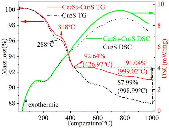
Figure 1.
Thermodynamic comparison of Cu2S and 6 wt% Ce2S3-Cu2S.
3.2. Effect of Ce2S3 Addition and Sintering Temperature on the Preparation of Ce2S3-Cu2S
Figure 2a shows the XRD pattern of Ce2S3-Cu2S sintered at 400 °C. The characteristic peaks of pure Cu2S indicate that the main components are hexagonal and monoclinic Cu2S. Compared to pure Cu2S, the diffraction peaks of Cu2S show shifts, most notably at 6 wt% addition, indicating lattice distortion caused by Ce3+ incorporation. Hexagonal Cu2S is temperature-dependent below 435 °C, with lattice constants ahex = 0.395 nm and chex = 0.675 nm [24]. The addition of 3 wt% and 4 wt% Ce2S3 resulted in the enhancement of characteristic peaks of monoclinic Cu2S. When Ce2S3 content increased to 5 wt% and 6 wt%, tetragonal Cu1.96S (PDF# 29-0578) [25,26] and orthorhombic Cu1.8S (PDF# 33-0489) emerge, respectively, indicating partial sulfur redistribution and phase segregation. The characteristic peak of Ce2S3 was also observed, indicating that the solution limit of Ce2S3 at 400 °C is 4 wt%. Excess Ce2S3 can promote the formation of Cu1.96S or Cu1.8S.
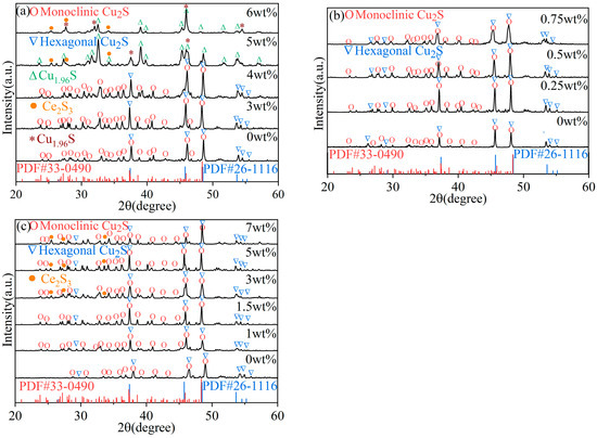
Figure 2.
XRD patterns of Ce2S3-Cu2S composite sintered at (a) 400 °C, (b) 500 °C, and (c) 600 °C.
To confirm the effect of temperature and trace amounts of Ce2S3 on the crystal structure of Cu2S, the addition of Ce2S3 was set at 0.25 wt%, 0.5 wt%, and 0.75 wt% during the sintering process at 500 °C. Unlike sintering at 400 °C, sintering pure Cu2S at 500 °C exhibits characteristic peaks of monoclinic and hexagonal phases (as shown in Figure 2b). Adding a small amount of Ce2S3 only alters the relative intensity of the characteristic peaks of the monoclinic and hexagonal phases without affecting the phase composition of the sintered product. In addition, the characteristic peak of monoclinic Cu2S with 0.5 wt% Ce2S3 added is significantly higher than that of monoclinic Cu2S with 0.25 wt% and 0.75 wt% Ce2S3 added.
The diffraction peaks of Cu2S are shifted with the increase of Ce2S3 addition at 600 °C (as shown in Figure 2c). Similar to 400 °C and 500 °C, the characteristic peak of pure Cu2S sintered at 600 °C corresponds to hexagonal and monoclinic structures. Unlike 400 °C, when the addition of Ce2S3 was 3 wt%, 5 wt%, and 7 wt%, the characteristic peaks of Ce2S3 were observed, but Cu1.96S and Cu1.8S were not formed, which is related to high-temperature sulfur loss. Compared to pure Cu2S, the diffraction peaks of Ce2S3-Cu2S are shifted to the left, which may be related to the lattice distortion caused by Ce2S3 addition. The similar hexagonal structure of Zn-doped Cu2S was confirmed by the CBD method [27]. An increase in Ti dopant concentration caused an increase in the crystallite size of Ti-doped CuS, which is different from Ce2S3-doped Cu2S [28]. Mn and Se co-doping is similar to Ce2S3-doped Cu2S, but there is a doping concentration limit of 0.05 [9].
Table 1 lists lattice constants of Ce2S3-Cu2S composites sintered at 400–600 °C. The structure of the low-temperature Cu2S phase is monoclinic, which was similar to the reported unit cell parameters (a = 15.25 Å, b = 11.88 Å, c = 13.49 Å) [24]. The lattice constants of Ce2S3-doped Cu2S exhibit significant dependence on both Ce2S3 addition and sintering temperature, as revealed by systematic XRD analysis. At 400 °C, increasing Ce2S3 content from 3 wt% to 6 wt% induces a phase transition from monoclinic to hexagonal and ultimately tetragonal structure (a = 4.0085Å). Theoretical calculations indicate that hexagonal Cu2S undergoes a high-temperature transformation to the cubic phase or Cu1.8S at 435 °C, but the addition of Ce2S3 prevents Cu2S from forming the cubic phase [29,30]. Elevated temperatures (500–600 °C) promote hexagonal phase stabilization. Notably, hexagonal phase constants remain stable (a ≈ 3.96Å, c ≈ 6.72Å) across temperatures, while the c-axis of monoclinic phase compresses by 0.9% at 600 °C compared to 400 °C, demonstrating temperature-induced anisotropic lattice distortion. The lattice constant of Ce2S3-doped Cu2S forming a hexagonal phase is smaller than the theoretical lattice constant (a = c = 4.097 Å) [30]. As the amount of Ce2S3 added increases, the lattice constant of monoclinic Cu2S increases at 500 °C. At 600 °C, Cu2S only undergoes a monoclinic-to-hexagonal structural phase transition and does not form a cubic phase even with a wide range of Ce2S3 addition (1–7 wt%). These coordinated variations confirm that Ce2S3 incorporation modifies Cu-S bond lengths through strain field effects while thermal energy controls phase competition kinetics.

Table 1.
Lattice constants of Ce2S3-Cu2S sintered at 400–600 °C.
Figure 3 shows SEM images of Ce2S3-Cu2S sintered at 400 °C. The sintered Cu2S exhibits an irregular oval shape with an average particle size in the range of 1.5–3 µm. The particle size of sintered Cu2S is smaller than that of ball-milled Cu2S powders (15 µm [31]. At low Ce2S3 addition (lower than 4 wt%), the Ce2S3-Cu2S has a relatively uniform structure, while as the Ce2S3 content increases to 5 wt%, the mixing of the Ce2S3 phase and Cu2S phase becomes non-uniform. On the other hand, the surface of the Ce2S3-Cu2S composite becomes rough and agglomerated, while finer particles emerge at 3 wt%. Optical microscope images of the surface of Ce2S3-Cu2S bulks were shown in Figure S1. Copper ion precipitation progressively diminishes and vanishes as more Ce2S3 is introduced. According to Table 2, both the actual contents of Ce element of 3 wt% and 4 wt% Ce2S3-Cu2S are less than the theoretical content, but 5 wt% and 6 wt% Ce2S3-Cu2S are higher than the theoretical content, which may be due to the uneven mixing.
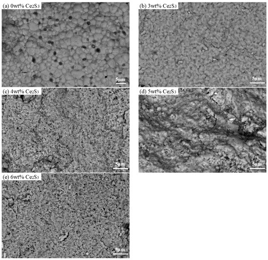
Figure 3.
SEM images of Ce2S3-Cu2S at 400 °C; (a) 0 wt%; (b) 3 wt%; (c) 4 wt%; (d) 5 wt%; (e) 6 wt%.
Table 2.
EDS elemental content of Ce2S3-Cu2S sintered at 400–600 °C.
Figure 4 shows the SEM images of sintered Cu2S and Ce2S3-Cu2S at 500 °C. As the sintering temperature increased from 400 °C to 500 °C, the grain size of Cu2S became larger; this is similar to the synthesis of Cu2S nanoparticles via cyclic microwave radiation [32]. All samples exhibit distinct particle boundaries, and grain size is about 5–10 µm. As the Ce2S3 content increases, the particle size becomes increasingly uniform, which indicates that the introduction of Ce2S3 can make the particles uniform.
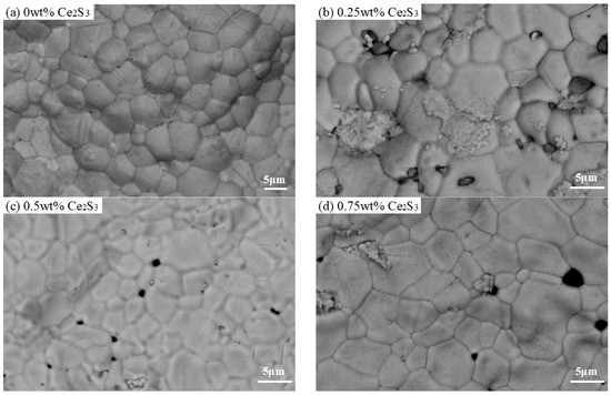
Figure 4.
SEM images of Ce2S3-Cu2S sintered at 500 °C; (a) 0 wt%; (b) 0.25 wt%; (c) 0.5 wt%; (d) 0.75 wt%.
Figure 5 shows SEM images of Ce2S3-Cu2S sintered at 600 °C. The 0 wt% Ce2S3-Cu2S has large holes appearing, and the surface is very rough, which may be due to insufficient grinding of raw materials. The 1 wt% Ce2S3-Cu2S has uniform particles of 15 μm with a certain number of pores remaining on the surface. With the gradual increase of Ce2S3 mass fraction, the 1.5 wt% Ce2S3-Cu2S has a smaller particle size of 3 μm with the number of pores further reduced. The 3 wt%, 5 wt%, and 7 wt% Ce2S3-Cu2S have a fibrous appearance on the surface, which may be due to the emergence of the new phase.
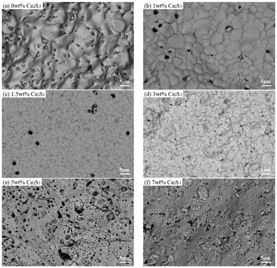
Figure 5.
SEM images of Ce2S3-Cu2S at 600 °C; (a) 0 wt%; (b) 1 wt%; (c) 1.5 wt%; (d) 3 wt%; (e) 5 wt%; (f) 7 wt%.
EDS map analysis of Ce2S3-Cu2S sintered at 400 °C, 500 °C, and 600 °C was shown in Figure S2. The EDS map analysis results indicate that Ce is uniformly distributed in the Cu2S matrix. Table 2 lists the EDS elemental content of Ce2S3-Cu2S sintered at 400–600 °C. There is a difference between the theoretical and actual Ce content of Ce2S3-Cu2S. The Ce contents of the 1 wt%, 1.5 wt%, and 7 wt% Ce2S3-Cu2S are larger than theoretical value. While Ce content of the 3 wt% and 5 wt% Ce2S3-Cu2S are smaller than the theoretical value. Besides, there are three significant trends regarding composition evolution. First, temperature plays a crucial role in elemental distribution. Increasing sintering temperature from 400 °C to 600 °C enhances Ce incorporation into the Cu2S matrix, as evidenced by the rise in actual Ce content (Ceact.) from 0.98 wt% to 2.03 wt% at a fixed 3 wt%. This temperature dependence demonstrates the thermally activated diffusion process of Ce species. Second, Ce2S3 concentration significantly affects phase composition. At 400 °C, while Ceact. increases linearly with nominal amount (0.98→9.02 wt% for 3→6 wt%), the values remain below theoretical predictions (Cetheo.), indicating incomplete solid solution formation. Remarkably, at 600 °C with 7 wt% Ce2S3, Ceact. (5.74 wt%) exceeds the theoretical value (5.27 wt%), suggesting possible Ce-rich surface segregation. Third, the Cu/S ratio shows systematic variations: undoped samples consistently exhibit Ceact. exceeding theoretical values, while doped samples show improved Cu stoichiometry at higher temperatures, demonstrating the effectiveness of Ce2S3 in suppressing Cu volatilization. These findings are consistent with the ionic size-mismatch driven substitution mechanism reported in rare-earth doped chalcogenides [33].
3.3. Magnetic Properties
Figure 6a shows the variation of magnetic susceptibility χ of 7 wt% Ce2S3-Cu2S in the temperature range from 0 K to 300 K and at 1000 Oe. The arrow points to the right side, which represents the reciprocal of the magnetic susceptibility. The fitting of the 1/χ curve conforms to the Curie–Weiss law, indicating that 7 wt% Ce2S3-Cu2S exhibits paramagnetic characteristics.
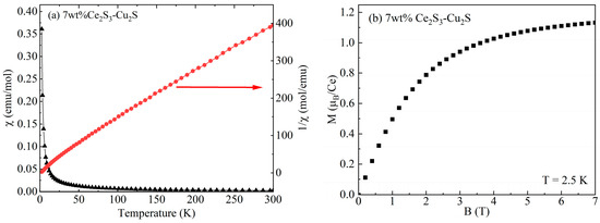
Figure 6.
Variation of magnetic susceptibility (a) and magnetization (b) of 7 wt% Ce2S3-Cu2S.
Figure 6b shows the variation of magnetization of 7 wt% Ce2S3-Cu2S measured at 2.5 K. The resulting saturation magnetization of Ce2S3-Cu2S is 1.2 µB/Ce, which is much lower than the theoretical magnetic moment of Ce3+ (2.45 µB) [34]. This may be caused by the coupling of the crystal field effect and the Kondo screening effect.
3.4. UV-VIS of Ce2S3-Cu2S
Figure 7 shows the UV-Vis Absorbance spectrum and the calculated optical energy gap plot of Ce2S3-Cu2S sintered at 400 °C. The absorption intensity increases with higher addition and stabilizes when addition exceeds 3 wt%. Cu2S displays its maximum absorption peak at 341 nm, while the peaks of Ce2S3-Cu2S shift to shorter wavelengths to varying extents. Similar behavior was observed by rare-earth Sm doping in Cu2SnSe3 and Gd doping on Cu2Sn1-xGdxS3 thin film system creates intermediate energy states that facilitate electron transitions [35,36]. From Figure 7, the Eg has been calculated to be 1.67 eV, 0.63 eV, 1.27 eV, 1.21 eV, and 1.12 eV for x = 0, 3, 4, 5, and 6 wt% Ce2S3, respectively. The value of 1.67 eV was consistent with the reported results [37,38]. When the addition of Ce2S3 exceeds 3 wt%, a second optical energy gap is present, with the second optical energy gap of 0.54 eV. This smaller optical energy gap of about 0.4–0.6 eV is between the Cu d valence and Cu s-like conduction bands, which is related to the hybridization of the Cu s and Cu d bands due to the symmetry breaking [30]. Combined with the XRD results (Figure 2), there are different crystal structures in the Ce2S3-Cu2S. The mixed hexagonal and monoclinic Cu2S phase determines both direct and indirect optical energy gap are present. The decrease in Eg with the increasing of the addition of Ce2S3 can be attributed to the 4f electrons (4f1) of Ce3+ ions. The 4f1 of Ce3+ ions are located at the middle of the optical energy gap of Cu2S semiconductors. When Ce3+ replaces Cu+ in the Cu2S lattice, its unfilled 4f electrons introduce new impurity levels into the original optical energy gap. As the Ce concentration increases, the distance between these localized 4f states decreases, causing the electron wave functions to overlap. This results in the isolated impurity levels expanding into a broader impurity band. The higher the doping concentration, the broader the impurity band, leading to a reduction in the measured Eg.
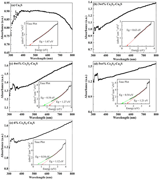
Figure 7.
UV-Vis Absorbance spectrum and the calculated optical energy gap plot of Ce2S3-Cu2S sintered at 400 °C; 0 wt% (a), 3 wt% (b), 4 wt% (c), 5 wt% (d), and 6 wt% (e).
The UV-Vis Absorbance spectrum and calculated optical energy gap of Ce2S3-Cu2S sintered at 600 °C were shown in Figure 8. All the peak and minimum absorption peaks of Ce2S3-Cu2S are in the same wavelength interval. The 5 wt% Ce2S3-Cu2S peak absorption occurs at wavelength 292 nm, while the absorption peak of Cu2S occurs at wavelength 296 nm. The highest absorption peaks of 1 wt% Ce2S3-Cu2S, 3 wt% Ce2S3-Cu2S, and 7 wt% Ce2S3-Cu2S appeared at wavelengths 298 nm, 302 nm, and 308 nm, respectively. The calculated optical energy gap of Cu2S is close to 1.91, and the optical energy gap of 3 wt% Ce2S3-Cu2S and 5 wt% Ce2S3-Cu2S are 1.78 eV and 1.72 eV, respectively. This non-monotonic trend mirrors the similar effects in doped chalcogenides of competing influences of strain and defect states [39]. There is the second optical energy gap (0.88 eV) for Cu2S and Ce2S3-Cu2S sintered at 600 °C. The small optical energy gap of sintered Ce2S3-Cu2S at 600 °C (0.88 eV) is higher than that of sintered Ce2S3-Cu2S at 400 °C (0.54 eV). This small optical energy gap increases from cubic to hexagonal to monoclinic [30]. Combined with Figure 2, the higher the sintering temperature is, the higher the relative content of monoclinic Cu2S is.
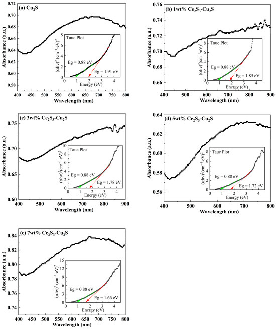
Figure 8.
UV-Vis Absorbance spectrum and the calculated optical energy gap plot of Ce2S3-Cu2S sintered at 600 °C; 0 wt% (a), 1 wt% (b), 3 wt% (c), 5 wt% (d), and 7 wt% (e).
3.5. Hardness and Density of Ce2S3-Cu2S
Figure 9a shows the hardness of Ce2S3-Cu2S. At 400 °C, the hardness increased significantly to 4 wt% Ce2S3 content and showed a decreasing trend as the content further increased. Combined with Figure 4, the microstructure of Ce2S3-Cu2S is denser with the increase of Ce2S3 addition. At 600 °C, the average hardness values show a decreasing trend between 1 wt% and 3 wt%, followed by a continuous slow increase. The hardness value of Ce2S3-Cu2S is lower than that of melt annealed treated Cu2S (Hv 1 GPa) [40]. At all Ce2S3 contents, the hardness at 400 °C is significantly higher than that at 600 °C. The hardness of the hexagonal phase Cu2S is lower than that of the tetragonal phase structure [41]. Pores exist at the grain boundaries of Ce2S3-Cu2S synthesized at 600 °C (Figure 5), which leads to a decrease in hardness and density.
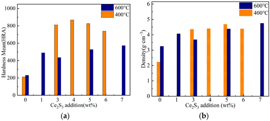
Figure 9.
Variation of hardness (a) and density (b) of Ce2S3-Cu2S.
The density of Ce2S3-Cu2S is plotted in Figure 9b. The density of Ce2S3-Cu2S is larger than that of pure Cu2S, which also proves that Ce2S3 addition increases the density of Ce2S3-Cu2S. The density of 3 wt% Ce2S3-Cu2S increases by 52.5% compared to that of Cu2S at 400 °C, and the density of 7 wt% Ce2S3-Cu2S at 600 °C increases by 34.2% compared to that of Cu2S.
3.6. Friction Properties
Figure 10 shows the variation of the friction coefficient of Ce2S3-Cu2S. As seen in Figure 10, both Cu2S and Ce2S3-Cu2S composites underwent rapid friction with the Cu ball friction vice at the initial stage of wear, resulting in a sharp increase in the coefficient of friction followed by stabilization. This is because the contact area between the Cu ball and the Ce2S3-Cu2S surface is small at the start. As the friction time increases, the contact area between Ce2S3-Cu2S and the Cu ball gradually increases, while the roughness of the contact surface decreases. This stabilizes the friction coefficient gradually. The average friction coefficients of 0 wt%, 1 wt%, 1.5 wt%, and 5 wt% are 0.7, 0.9, 0.65, and 0.6, respectively. The antifriction effect of the Ce2S3-Cu2S was similar to Ni55/Cu2S composite fabricated by laser cladding and low temperature ion sulfurizing, which is related to the oxidative protection of Cu2S and the bonding precipitation of Cu [42]. The 1 wt% Ce2S3 initially increases the friction coefficient of Cu2S due to improved hardness and wear resistance. However, at higher additions, the friction coefficient begins to decline.
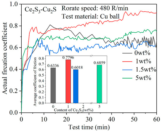
Figure 10.
Average coefficient of friction and change of friction coefficient of Ce2S3-Cu2S.
Figure 11 shows SEM and EDS images of the abrasion mark morphology. The friction surface at the friction groove is smoother than the surface before friction, but some material flaking occurs locally, which indicates that the material wear mechanism is a combination of abrasive wear and adhesive wear, and the EDS shows that the abrasive particles are non-Cu particles, which suggests that the abrasive particles come from the material rather than from the Cu ball friction substitutes. The shallow scratches in the SEM images may be caused by abrasive wear occurring on the micro-bumps on the surface of the material. In addition, the corrugated cracks at 1 wt%, 1.5 wt%, and 5 wt% of the friction grooves are oriented perpendicular to the friction direction, which may be the result of grinding cracks caused by tensile stresses on the surface layer of the material or the stress release in the internal tissues during the friction process.
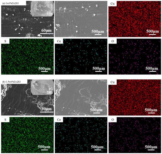
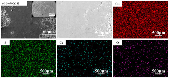
Figure 11.
SEM and EDS images of wear scar of Ce2S3-Cu2S; (a) 1 wt%; (b) 1.5 wt%; (c) 5 wt%.
Table 3 shows the EDS elemental distribution of Ce2S3-Cu2S. It can be clearly seen that there is still a distribution of Ce elements in the friction traces after friction, and the atomic percentage of Ce elements before and after friction is basically unchanged with the increase of the addition. In addition, the atomic percentage of Ce elements before and after friction is generally higher than that of S. Ce2S3 exists in the form of agglomerates, and a small amount of oxidation occurs during friction to form less oxide film on the surface of the material, thus improving the friction performance of the doped material.
Table 3.
EDS element distribution of Ce2S3-Cu2S grinding marks.
4. Discussions
Ce2S3 can optimize the thermal stability and mechanical properties of modified Cu2S by altering its phase composition and microstructure. Adding 5 wt% or 6 wt% Ce2S3 at 400 °C can generate copper-rich phases Cu1.96S or Cu1.8S. This differs from the mechanism of transition metal element doping (Co [43], Ag [10], Mo [44], Mn [45], Zn [27], Bi [46], P, As, Sb [11]) and oxide (CuO [23], Fe3O4 [47]) modification of Cu2S. Before Co doping, Cu2S is a mixture of monoclinic and hexagonal phases, which becomes a monoclinic single phase after Co doping (Figure 1 of Ref. [43]). All phases of Ag-doped Cu2S have a tetragonal structure, and Cu1.96S and CuAgS appear when the addition amount is 2 wt% [10]. The phase composition of Mo-doped Cu2S is a mixture of tetragonal and monoclinic phases, and the phase composition remains unchanged before and after Mn doping [44]. Both 5% and 10% Mn-doped Cu2S form hexagonal structures [45]. Zn-doped Cu2S [27] and 3% Bi-doped Cu2S [46] only form an amorphous phase. P, As, Sb, and Bi-doped Cu2S form monoclinic phases and trace amounts of copper compounds as secondary phases both before and after sintering [11]. Both CuO [23] and Fe3O4 [47] modified Cu2S are modified by dispersing the second phase.
The advantage of Ce2S3-modified Cu2S is that the anions are identical. At low Ce2S3 addition levels, Ce2S3 may be incorporated into the hexagonal Cu2S crystal lattice, achieving low-concentration doping. When the Ce2S3 addition reaches the saturation limit, Ce2S3 is dispersed at the crystal lattice through interface engineering, improving the grain structure of Cu2S. This is similar to the modification of Cu2S by graphene [48] and Bi2S3 [49]. Previous studies have primarily focused on the effect of dopant concentration on Cu2S performance [45]. This study investigates the synergistic effect of sintering temperature and dopant concentration. As sintering temperature increases, Cu and S ion losses create numerous vacancies (Figure 3, Figure 4 and Figure 5). Adding an appropriate amount of Ce2S3 can suppress copper ion precipitation at the macroscopic level. Optical micrographs in Figure S1 show that copper precipitation on the surface of the sintered sample disappears. Microscopically, adding Ce2S3 at 400 °C refines the grain size (Figure 3). As the sintering temperature increases to 600 °C, adding 1.5 wt% and 3 wt% Ce2S3 significantly outperforms other addition amounts (Figure 5).
Figure 12 summarizes and compares the relationship between the Eg of Cu2S and the addition of different dopant elements. As shown in the figure, Ce2S3 doping can effectively adjust the optical energy gap of Cu2S. Overall, the Eg decreases as the addition of Ce2S3 increases. The Eg increases with rising sintering temperature. This is like the effect of doping levels on the optical energy gap in Bi-doped Cu2S [46] and Mn-doped Cu2S [45]. It is opposite to the trend observed in Ti-doped CuS [28], Zn [27], and CuO-doped Cu2S [23], where the optical energy gap varies with doping level. Ce2S3 regulates the optical energy gap of Cu2S primarily by forming hybridized bands through the 4f electrons (4f1) of Ce3+ ions.
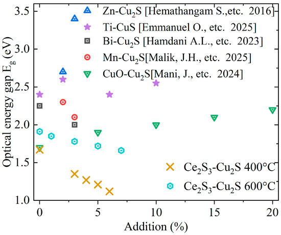
Figure 12.
Comparison Eg of Cu2S and doped-Cu2S [23,27,28,45,46].
5. Conclusions
The effects of sintering temperature and Ce2S3 addition on the stability and mechanical properties of Cu2S compound were studied. The conclusions are mainly in the following four aspects:
- (1)
- Ce2S3 addition effectively enhances the high-temperature stability of Cu2S by reducing mass loss. The sintering temperature and Ce2S3 addition significantly affect the crystal structure of Cu2S. The microstructure of Ce2S3-Cu2S sintered at 400 °C is denser than that sintered at 600 °C.
- (2)
- According to magnetic experiments, 7 wt% Ce2S3-Cu2S has a relatively low saturation magnetization of 1.2 µB/Ce and behaves paramagnetically. Ce2S3-Cu2S sintered at 400 °C has a narrower band gap than that sintered at 600 °C.
- (3)
- The hardness value increases and then decreases with the increase of Ce2S3 addition. Compared to pure Cu2S, the density values with the addition of 3 wt% Ce2S3 and 7 wt% Ce2S3 increased by 52.5% and 34.2%, respectively.
- (4)
- As the addition of Ce2S3 increases, the friction coefficients of Ce2S3-Cu2S first increase and then decrease, reaching a maximum for 1 wt% Ce2S3-Cu2S. The wear mechanism of Ce2S3-Cu2S is the combined effect of abrasive and adhesive wear.
Supplementary Materials
The following supporting information can be downloaded at: https://www.mdpi.com/article/10.3390/coatings15101135/s1, Figure S1: Optical microscope images of the surface of Ce2S3-Cu2S bulks; as the amount of Ce2S3 added increases, copper ion precipitation gradually weakens and disappears. Figure S2: EDS map analysis of Ce2S3-Cu2S sintered at 400°C, 500 °C and 600 °C; EDS map analysis results indicate that Ce is uniformly distributed in the Cu2S matrix.
Author Contributions
Conceptualization, Y.C. and L.L.; methodology, B.S., Y.W., Z.S. and L.L.; data curation, B.S., Y.W. and L.L.; writing—original draft preparation, B.S., Y.W., Y.C. and L.L.; writing—review and editing, Y.C. and L.L.; project administration, Y.C. and M.H.; funding acquisition, Y.C. and L.L. All authors have read and agreed to the published version of the manuscript.
Funding
This research was funded by the Natural Science Foundation of Henan Province, grant numbers 242300421464 and 252300420062; the Doctoral Special Fund Project of Nanyang Normal University, grant number 2024ZX025; and the Cultivation Project of the National Natural Science Foundation of Nanyang Normal University, grant numbers 2024PY023 and 2023PY011.
Institutional Review Board Statement
Not applicable.
Informed Consent Statement
Not applicable.
Data Availability Statement
The data that supports the findings of this study are available on reasonable requests from the corresponding author, Liang Li.
Conflicts of Interest
Liang Li was employed by the company Jinguan Electric Co., Ltd. The remaining authors declare that the research was conducted in the absence of any commercial or financial relationships that could be construed as a potential conflict of interest.
References
- Hamida, A.; Al-Maiyaly, B. Synthesis and characterization of Cu2S: Al thin films for solar cell applications. Chalcogenide Lett. 2022, 19, 579–590. [Google Scholar] [CrossRef]
- Zhao, B.; Long, X.; Zhao, Q.; Shakouri, M.; Feng, R.; Lin, L.; Zeng, Y.; Zhang, Y.; Fu, X.Z.; Luo, J.L. In situ self-heterogenization of Cu2S/CuS nanostructures with modulated d band centers for promoting photocatalytic degradation and hydrogen evolution performances. Mater. Today Nano 2023, 23, 100362. [Google Scholar] [CrossRef]
- Jiang, Y.; Xu, Y.; Zhang, Q.; Zhao, X.; Xiao, F.; Wang, X.; Ma, G. Templated synthesis of Cu2S hollow structures for highly active ozone decomposition. Catalysts 2024, 14, 153. [Google Scholar] [CrossRef]
- Yu, J.; Liu, X.; Hu, H.; Jiang, Y.; Zhuang, H.L.; Li, H.; Su, B.; Li, J.W.; Han, Z.; Wang, Z. Ultralow thermal conductivity and high ZT of Cu2Se-based thermoelectric materials mediated by TiO2−n nanoclusters. Joule 2024, 8, 2652–2666. [Google Scholar] [CrossRef]
- Yan, Y.; Bai, Y.; Ouyang, T.; Li, X.; Wang, X.; Jiang, X.; Wang, W.; Cai, X.; Cai, J.; Tan, H. The thermoelectric properties of Cu2S are enhanced by doping tin with hydrothermal method. J. Mater. Sci. Mater. Electron. 2024, 35, 1110. [Google Scholar] [CrossRef]
- Qiu, P.; Zhu, Y.; Qin, Y.; Shi, X.; Chen, L. Electrical and thermal transports of binary copper sulfides CuxS with x from 1.8 to 1.96. APL Mater. 2016, 4, 104805. [Google Scholar] [CrossRef]
- Zheng, L.J.; Zhang, B.P.; Li, H.-Z.; Pei, J.; Yu, J.B. CuxS superionic compounds: Electronic structure and thermoelectric performance enhancement. J. Alloys Compd. 2017, 722, 17–24. [Google Scholar] [CrossRef]
- Li, C.Q.; Wang, J.J. Copper sulfide based photocatalysts, electrocatalysts and photoelectrocatalysts: Innovations in structural modulation and application. Small 2024, 20, 2404798. [Google Scholar] [CrossRef] [PubMed]
- Gong, C.; Zeng, Z.; Sun, X.; Luo, C.; Chen, H. Mn-doping method boosts Se doping concentration in Cu2S towards high thermoelectric performance. J. Mater. Chem. C 2025, 13, 326–333. [Google Scholar] [CrossRef]
- Yue, Z.; Zhou, W.; Ji, X.; Zhang, F.; Guo, F. Enhanced thermoelectric properties of Ag doped Cu2S by using hydrothermal method. J. Alloys Compd. 2022, 919, 165830. [Google Scholar] [CrossRef]
- Nieroda, P.; Leszczyński, J.; Kapera, K.; Rutkowski, P.; Ziewiec, K.; Szymańska, A.; Kruszewski, M.J.; Rudnik, M.; Koleżyński, A. Thermoelectric properties of Cu2S doped with P, As, Sb and Bi—Theoretical and experimental studies. Materials 2024, 17, 5440. [Google Scholar] [CrossRef]
- Shen, F.; Zheng, Y.; Miao, L.; Liu, C.; Gao, J.; Wang, X.; Liu, P.; Yoshida, K.; Cai, H. Boosting high thermoelectric performance of Ni-Doped Cu1.9S by significantly reducing thermal conductivity. ACS Appl. Mater. Interfaces 2020, 12, 8385–8391. [Google Scholar] [CrossRef]
- Mulla, R.; Rabinal, M. CuO/CuxS composites fabrication and their thermoelectric properties. Mater. Renew. Sustain. Energy 2021, 10, 3. [Google Scholar] [CrossRef]
- Pokhrel, S.; Martuza, M.A.; Groeneveld, J.D.; Schowalter, M.; Rosenauer, A.; Birkenstock, J.; Mädler, L. Gas phase synthesis of mixed Cu1.8S-ZnS particles and the terminal phases in the reducing atmosphere. Powder Technol. 2025, 465, 121318. [Google Scholar] [CrossRef]
- Mikuła, A.; Koleżyński, A. First principles studies of Fe-doped Cu2S—Theoretical investigation. Solid State Ion. 2019, 334, 36–42. [Google Scholar] [CrossRef]
- Zou, L.; Zhang, B.P.; Ge, Z.H.; Gao, C.; Zhang, D.B.; Liu, Y.C. Size effect of SiO2 on enhancing thermoelectric properties of Cu1.8S. Phys. Status Solidi (A) 2013, 210, 2550–2555. [Google Scholar] [CrossRef]
- Meng, Q.L.; Kong, S.; Huang, Z.; Zhu, Y.; Liu, H.C.; Lu, X.; Jiang, P.; Bao, X. Simultaneous enhancement in the power factor and thermoelectric performance of copper sulfide by In2S3 doping. J. Mater. Chem. A 2016, 4, 12624–12629. [Google Scholar] [CrossRef]
- Qin, P.; Ge, Z.H.; Chen, Y.X.; Chong, X.; Feng, J.; He, J. Achieving high thermoelectric performance of Cu1.8S composites with WSe2 nanoparticles. Nanotechnology 2018, 29, 345402. [Google Scholar] [CrossRef] [PubMed]
- Qin, P.; Ge, Z.H.; Feng, J. Enhanced thermoelectric properties of SiC nanoparticle dispersed Cu1.8S bulk materials. J. Alloys Compd. 2017, 696, 782–787. [Google Scholar] [CrossRef]
- Kharboot, L.H.; Ojaomo, K.E. Advancing quantum dot-sensitized solar cells: Transition metal-sulfide-based counter electrodes for high-efficiency and stable photovoltaics. Quantum J. Eng. Sci. Technol. 2025, 6, 121–133. [Google Scholar] [CrossRef]
- Arif Khalil, R.; Hussain, M.I.; Imran, M.; Hussain, F.; Saeed, N.; Murtaza, G.; Rana, A.M.; Mahata, C. First-principles simulation of structural, electronic and optical properties of cerium trisulfide (Ce2S3) compound. J. Electron. Mater. 2021, 50, 1637–1643. [Google Scholar] [CrossRef]
- Huang, L.; Lu, H. Electronic structure of cerium: A comprehensive first-principles study. Phys. Rev. B 2019, 99, 045122. [Google Scholar] [CrossRef]
- Mani, J.; Radha, S.; Prita, F.J.; Rajkumar, R.; Arivanandhan, M.; Anbalagan, G. Enhancing the thermoelectric performance of Cu2S/CuO nanocomposites through energy-filtering effect and phonon scattering. J. Inorg. Organomet. Polym. Mater. 2024, 34, 1548–1563. [Google Scholar] [CrossRef]
- Sands, T.; Washburn, J.; Gronsky, R. High resolution observations of copper vacancy ordering in chalcocite (Cu2S) and the transformation to djurleite (Cu1.97 to 1.94S). Phys. Status Solidi (A) 1982, 72, 551–559. [Google Scholar] [CrossRef][Green Version]
- Zhang, R.; Pei, J.; Han, Z.J.; Wu, Y.; Zhao, Z.; Zhang, B.P. Optimal performance of Cu1.8S1−xTex thermoelectric materials fabricated via high-pressure process at room temperature. J. Adv. Ceram. 2020, 9, 535–543. [Google Scholar] [CrossRef]
- Bronusiene, A.; Ancutiene, I. Elemental sulfur as a precursor for CuxS layer formation. Chalcogenide Lett. 2018, 15, 483–489. [Google Scholar]
- Hemathangam, S.; Thanapathy, G.; Muthukumaran, S. Tuning of band gap and photoluminescence properties of Zn doped Cu2S thin films by CBD method. J. Mater. Sci. Mater. Electron. 2016, 27, 2042–2048. [Google Scholar] [CrossRef]
- Okechukwu, E.O.; Ekpunobi, A.J.; Azubogu, A.; Onuigbo, E.; Anusiuba, O.; Nwodo, A.; Jeroh, D.M.; Muomeliri, C.B.; Okafor, C.E.; Ozobialu, L. Investigating the doping effects on the optical, electrical, structural, morphological, elemental composition, and magnetic properties of electrodeposited Ti-doped CuS thin films. Mater. Nanosci. 2025, 12, 1191. [Google Scholar] [CrossRef]
- Jie, Y.; Zhang, S.; Houb, H.; Xiec, L. Theoretical study on structural, electronic structure, elastic and optical properties of α-Cu2S. Chalcogenide Lett. 2023, 20, 903–913. [Google Scholar] [CrossRef]
- Lukashev, P.; Lambrecht, W.R.; Kotani, T.; Van Schilfgaarde, M. Electronic and crystal structure of Cu2−xS: Full-potential electronic structure calculations. Phys. Rev. B-Condens. Matter Mater. Phys. 2007, 76, 195202. [Google Scholar] [CrossRef]
- Kim, J.S.; Kim, D.-Y.; Cho, G.B.; Nam, T.H.; Kim, K.W.; Ryu, H.S.; Ahn, J.H.; Ahn, H.J. The electrochemical properties of copper sulfide as cathode material for rechargeable sodium cell at room temperature. J. Power Sources 2009, 189, 864–868. [Google Scholar] [CrossRef]
- Mousavi-Kamazani, M.; Salavati-Niasari, M.; Sadeghinia, M. Synthesis and characterization of Cu2S nanostructures via cyclic microwave radiation. Superlattices Microstruct. 2013, 63, 248–257. [Google Scholar] [CrossRef]
- Mitchell, K.; Ibers, J.A. Rare-earth transition-metal chalcogenides. Chem. Rev. 2002, 102, 1929–1952. [Google Scholar] [CrossRef]
- Klicpera, M. Electron Properties of the Substituted Cerium Compounds. Ph.D. Thesis, Charles University, Prague, Czech Republic, 2015. [Google Scholar]
- Gurung, T.; Jagan, R.; Shanubhogue, D.; Poojitha, G.; Rao, A. Enhancement in power factor through rare-earth samarium doping in Cu2SnSe3 system. Phys. Scr. 2024, 99, 105908. [Google Scholar] [CrossRef]
- Baturay, Ş.; Gezgin, S.Y.; Köylü, M.Z.; Kabatas, M.A.B.-M.; Kiliç, H.Ş. Influence of Gd doping on Cu2Sn1−xGdxS3 thin film solar cell. iScience 2025, 28, 112597. [Google Scholar] [CrossRef]
- Pop, A.; Popescu, V.; Danila, M.; Batin, M. Optical properties of cuxs nano-powders. Chalcogenide Lett. 2011, 8, 363–370. [Google Scholar]
- Yu, X.; An, X. Controllable hydrothermal synthesis of Cu2S nanowires on the copper substrate. Mater. Lett. 2010, 64, 252–254. [Google Scholar] [CrossRef]
- Rasal, A.S.; Chang, T.W.; Korupalli, C.; Chang, J.Y. Composition engineered ternary copper chalcogenide alloyed counter electrodes for high-performance and stable quantum dot-sensitized solar cells. Compos. Part B Eng. 2022, 232, 109610. [Google Scholar] [CrossRef]
- Zhao, L. Investigation on the Electronic Structures, Hardness and Thermoelectric Properties of Superionic Thermoelectric Materials. Ph.D. Thesis, University of Wollongong, Wollongong, Australia, 2016. [Google Scholar]
- Sueyoshi, H.; Yamano, Y.; Inoue, K.; Maeda, Y.; Yamada, K. Mechanical properties of copper sulfide-dispersed lead-free bronze. Mater. Trans. 2009, 50, 776–781. [Google Scholar] [CrossRef]
- Zhao, J.; Wang, Y.; Han, B.; Li, M.; Cui, G. Antifriction effects of Cu2S film on Ni-based MMC coating. Surf. Coat. Technol. 2017, 315, 391–398. [Google Scholar] [CrossRef]
- Yang, L.; Yao, Y.; Zhu, G.; Ma, M.; Wang, W.; Wang, L.; Zhang, H.; Zhang, Y.; Jiao, Z. Co doping of worm–like Cu2S: An efficient and durable heterogeneous electrocatalyst for alkaline water oxidation. J. Alloys Compd. 2018, 762, 637–642. [Google Scholar] [CrossRef]
- Xie, Y.; Huang, J.; Xu, R.; He, D.; Niu, M.; Li, X.; Xu, G.; Cao, L.; Feng, L. Mo-doped Cu2S multilayer nanosheets grown in situ on copper foam for efficient hydrogen evolution reaction. Molecules 2022, 27, 5961. [Google Scholar] [CrossRef]
- Malik, J.H.; Islam, I.; Kaur, K.; Ali, A.M.; Khandy, S.A. Electronic and photoluminescent properties of Mn-doped Cu2S nanostructures for possible photocatalytic applications. Inorg. Chem. Commun. 2025, 179, 114814. [Google Scholar] [CrossRef]
- AL-Hamdani, A.A.H.; AL-Maiyaly, B.K. Growth and characterization of bi doped Cu2S nano crystalline thin films. AIP Conf. Proc. 2023, 2769, 020048. [Google Scholar] [CrossRef]
- Yang, T.Y.; Wang, Z.Y.; Yan, X.; Wang, C.Y.; Zhang, Y.X.; Ge, Z.H.; Feng, J. Excellent thermoelectric performance realized in copper sulfide magnetic nanocomposites via modified solid states reaction. Adv. Sci. 2025, 12, 2409494. [Google Scholar] [CrossRef]
- Tang, H.; Sun, F.H.; Dong, J.F.; Zhuang, H.L.; Pan, Y.; Li, J.F. Graphene network in copper sulfide leading to enhanced thermoelectric properties and thermal stability. Nano Energy 2018, 49, 267–273. [Google Scholar] [CrossRef]
- Zhang, Y.X.; Ge, Z.H.; Feng, J. Enhanced thermoelectric properties of Cu1.8S via introducing Bi2S3 and Bi2S3@ Bi core-shell nanorods. J. Alloys Compd. 2017, 727, 1076–1082. [Google Scholar] [CrossRef]
Disclaimer/Publisher’s Note: The statements, opinions and data contained in all publications are solely those of the individual author(s) and contributor(s) and not of MDPI and/or the editor(s). MDPI and/or the editor(s) disclaim responsibility for any injury to people or property resulting from any ideas, methods, instructions or products referred to in the content. |
© 2025 by the authors. Licensee MDPI, Basel, Switzerland. This article is an open access article distributed under the terms and conditions of the Creative Commons Attribution (CC BY) license (https://creativecommons.org/licenses/by/4.0/).