
Effect of Nitrogen Ratio in Sputtering on the Quality of Film Formation and Electron Emission Properties of Nitride Films

Abstract
1. Introduction
2. Experimental Methods
2.1. Film Preparation by Magnetron Sputtering
2.2. Physical Characterization
2.3. Electron Emission Coefficient Characterization
3. Results and Discussion
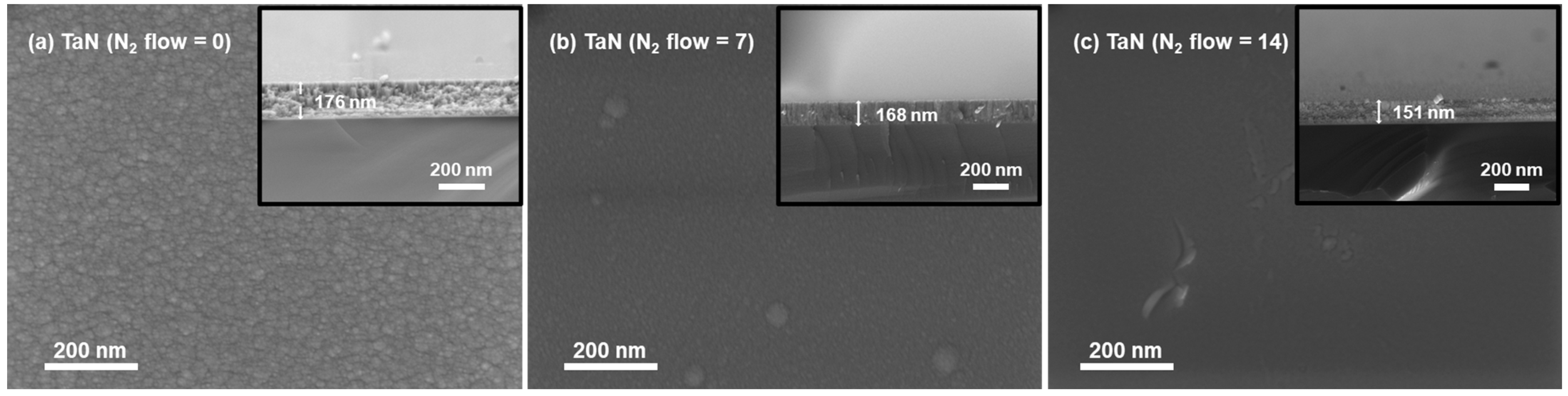
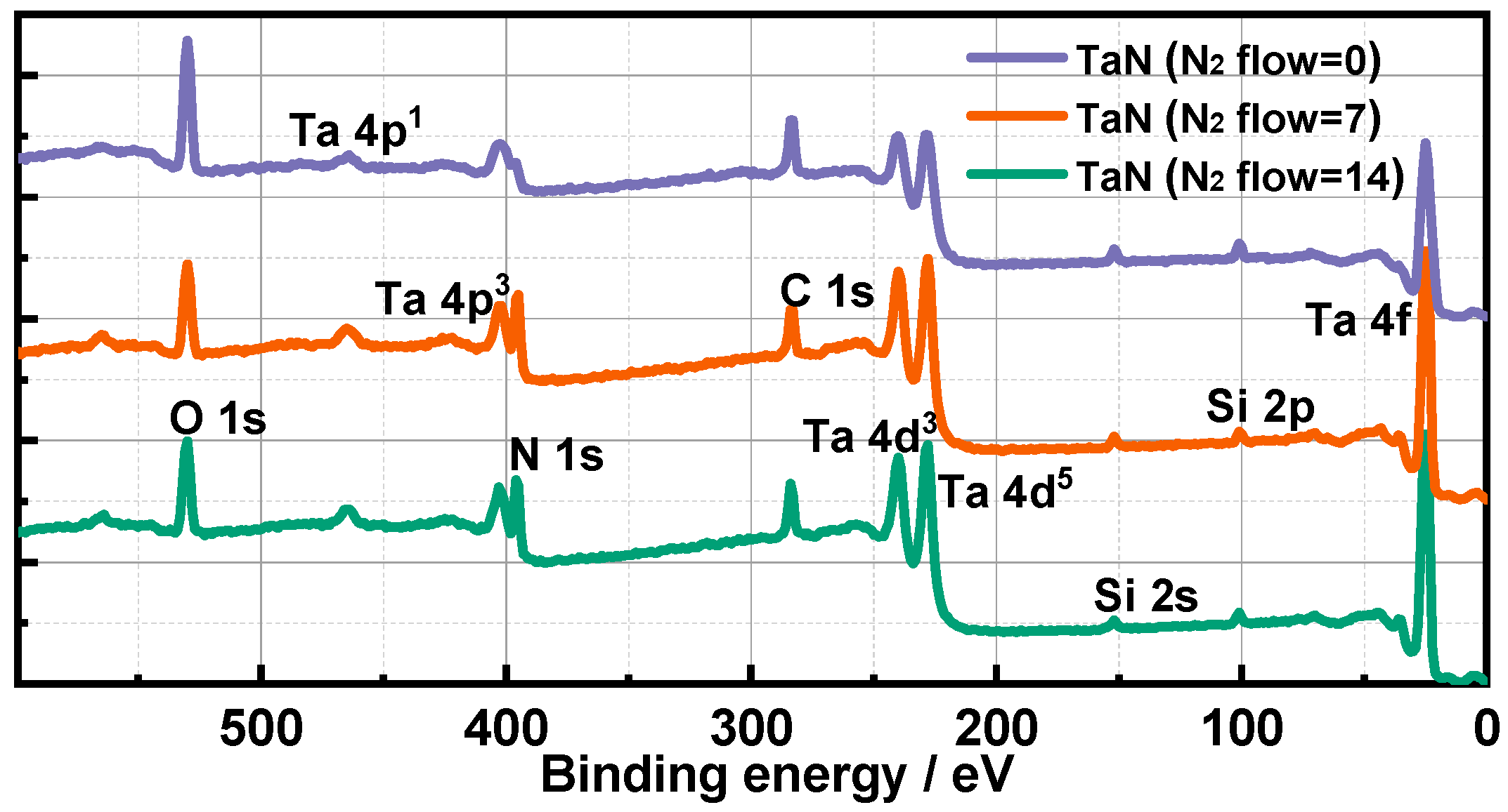
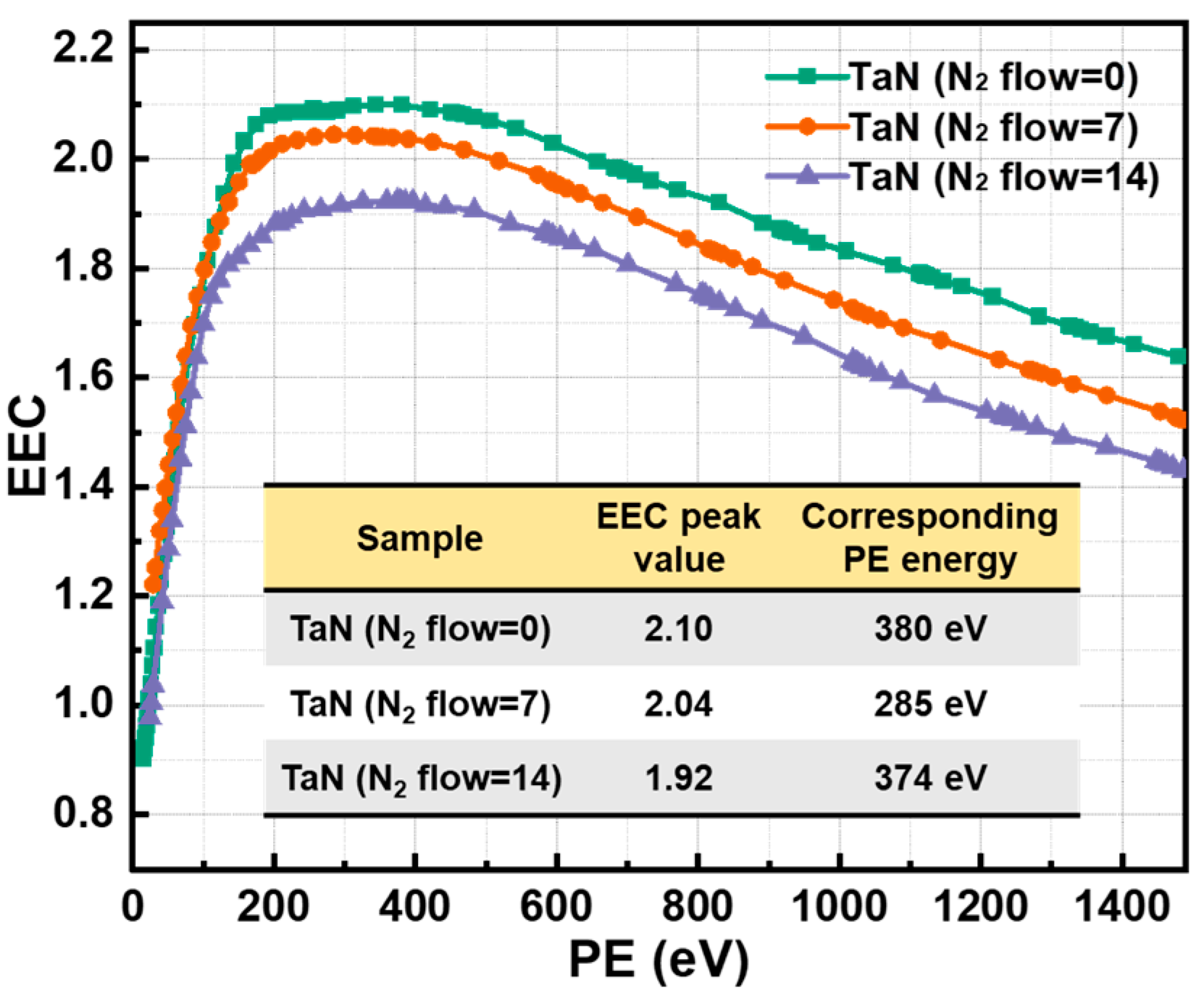
3.1. Morphology, Surface Components and EEC Results of TaN Films
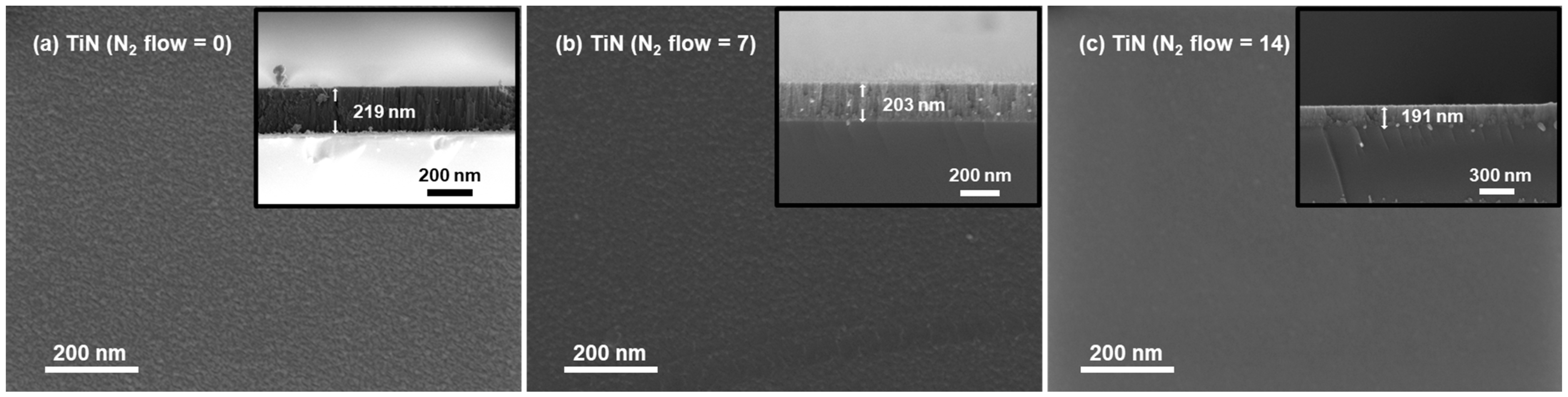
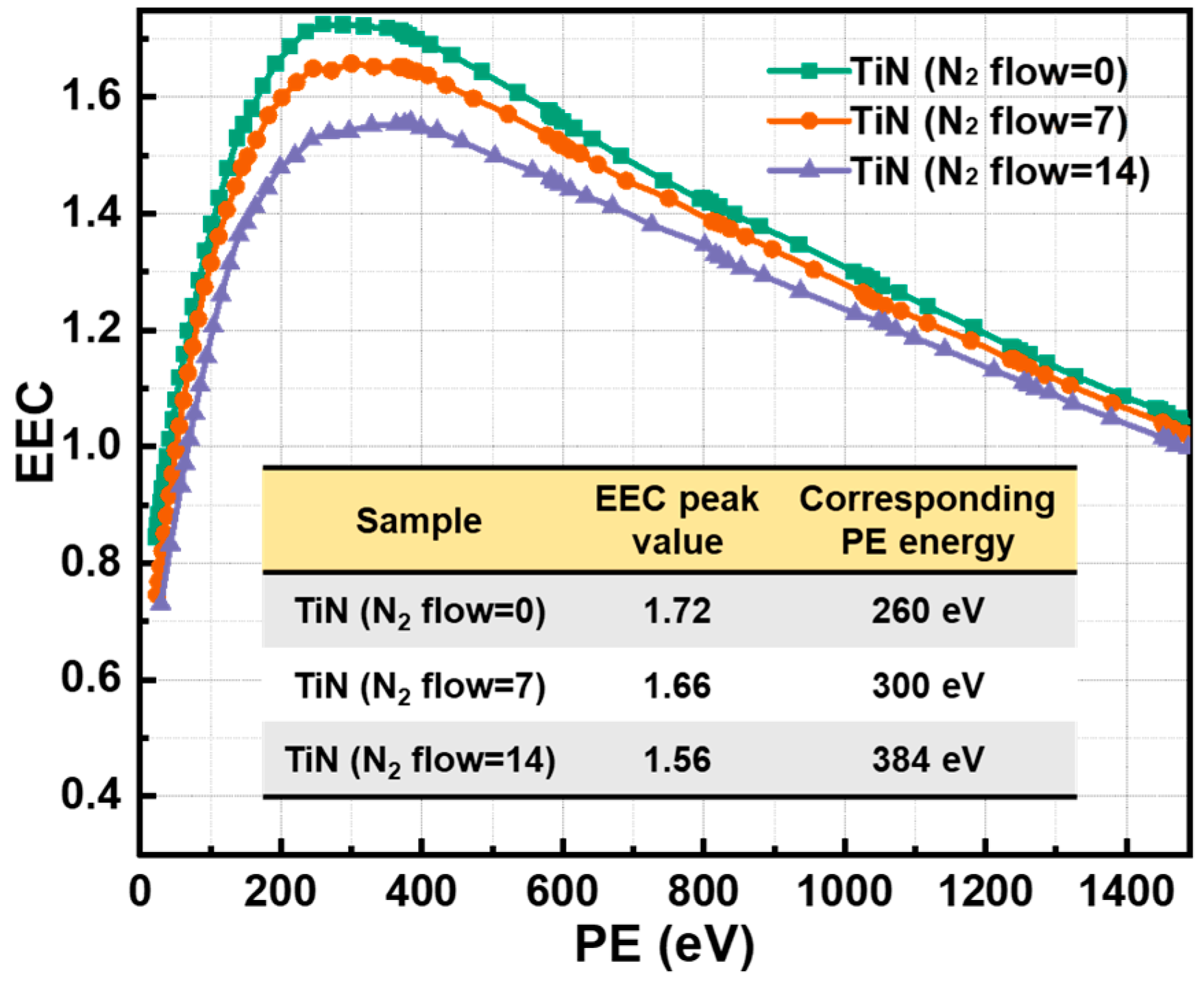
3.2. Morphology, Surface Components and EEC Results of TiN Films
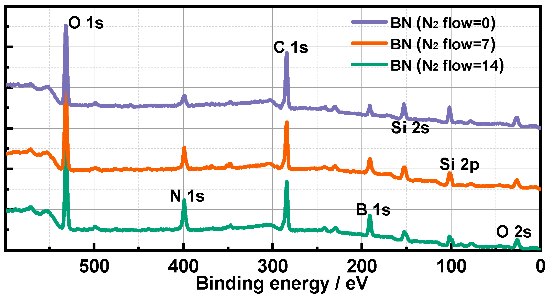
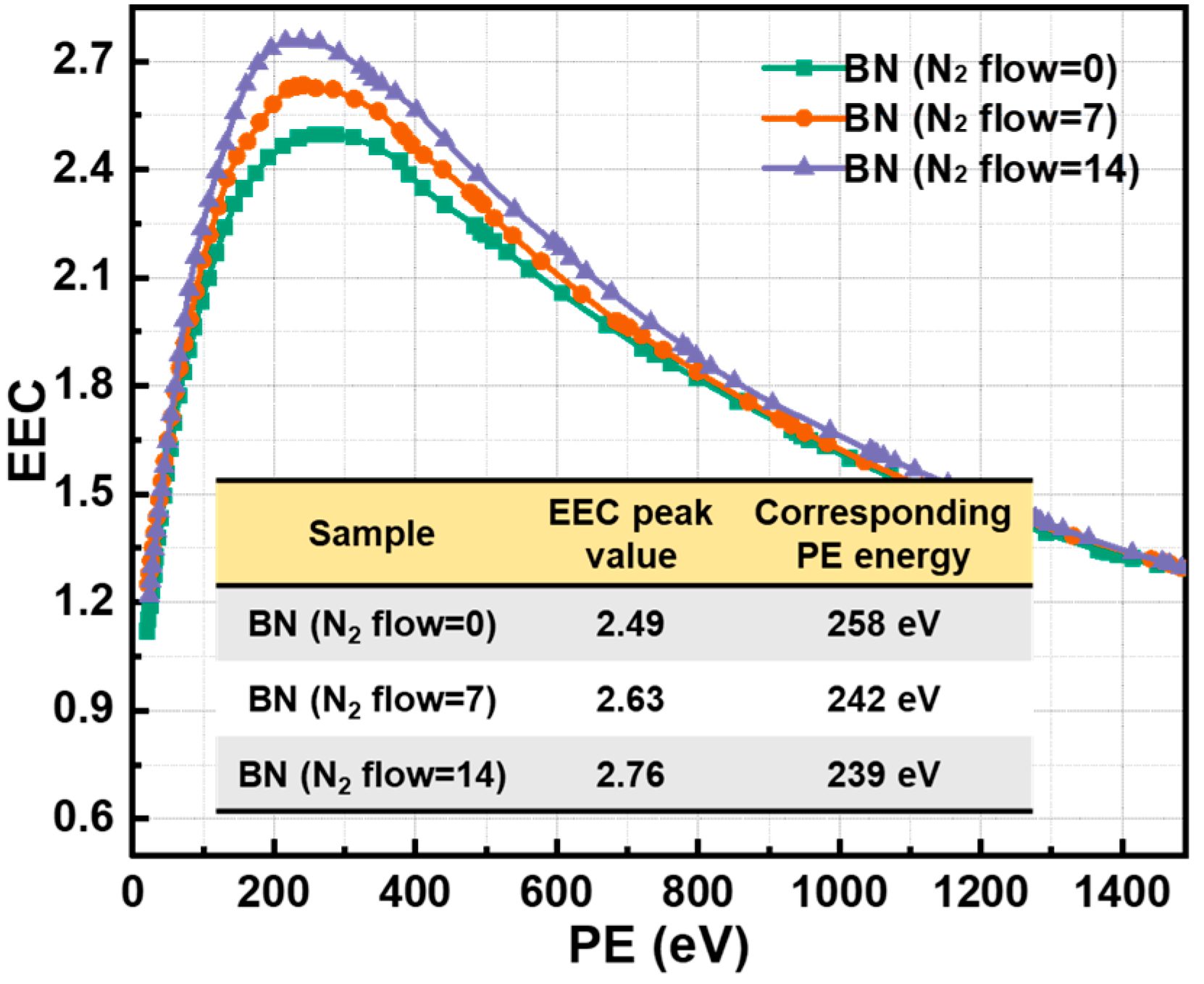
3.3. Morphology, Surface Components and EEC Results of BN Films
4. Conclusions
Author Contributions
Funding
Institutional Review Board Statement
Informed Consent Statement
Data Availability Statement
Conflicts of Interest
References
- Pihosh, Y.; Minegishi, T.; Nandal, V.; Higashi, T.; Katayama, M.; Yamada, T.; Sasaki, Y.; Seki, K.; Suzuki, Y.; Nakabayashi, M.; et al. Ta3N5-nanorods enabling highly efficient water oxidation via advantageous light harvesting and charge collection. Energy Environ. Sci. 2020, 13, 1519–1530. [Google Scholar] [CrossRef]
- Ding, C.; Shi, J.; Wang, Z.; Li, C. Photoelectrocatalytic Water Splitting: Significance of Cocatalysts, Electrolyte, and Interfaces. ACS Catal. 2016, 7, 675–688. [Google Scholar] [CrossRef]
- Li, Y.B.; Takata, T.; Cha, D.; Takanabe, K.; Minegishi, T.; Kubota, J.; Domen, K. Vertically aligned Ta3N5 nanorod arrays for solar-driven photoelectrochemical water splitting. Adv. Mater. 2013, 25, 125–131. [Google Scholar] [CrossRef] [PubMed]
- Jiang, C.M.; Wagner, L.I.; Horton, M.K.; Eichhorn, J.; Rieth, T.; Kunzelmann, V.F.; Kraut, M.; Li, Y.B.; Persson, K.A.; Sharp, I.D. Metastable Ta2N3 with highly tunable electrical conductivity via oxygen incorporation. Mater. Horiz. 2021, 8, 1744–1755. [Google Scholar] [CrossRef]
- Patsalas, P.; Kalfagiannis, N.; Kassavetis, S. Optical Properties and Plasmonic Performance of Titanium Nitride. Materials 2015, 8, 3128–3154. [Google Scholar] [CrossRef]
- Chaudhry, A.; Mansoor, B.; Mungole, T.; Ayoub, G.; Field, D.P. Corrosion mechanism in PVD deposited nano-scale titanium nitride thin film with intercalated titanium for protecting the surface of silicon. Electrochim. Acta 2018, 264, 69–82. [Google Scholar] [CrossRef]
- Chin, Y.-L.; Chou, J.-C.; Lei, Z.-C.; Sun, T.-P.; Chung, W.-Y.; Hsiung, S.-K. Titanium Nitride Membrane Application to Extended Gate Field Effect Transistor pH Sensor Using VLSI Technology. Jpn. J. Appl. Phys. 2001, 40, 6311. [Google Scholar] [CrossRef]
- Shayeganfar, F.; Shahsavari, R. Electronic and pseudomagnetic properties of hybrid carbon/boron-nitride nanomaterials via ab-initio calculations and elasticity theory. Carbon 2016, 99, 523–532. [Google Scholar] [CrossRef]
- Zhou, J.; Wang, Q.; Sun, Q.; Jena, P. Electronic and magnetic properties of a BN sheet decorated with hydrogen and fluorine. Phys. Rev. B 2010, 81, 085442. [Google Scholar] [CrossRef]
- Backfish, M.; Eldred, J.; Tan, C.-Y.; Zwaska, R. Beam Tests of Beampipe Coatings for Electron Cloud Mitigation in Fermilab Main Injector. IEEE Trans. Nucl. Sci. 2015, 63, 957–964. [Google Scholar] [CrossRef]
- Kirby, R.; King, F. Secondary electron emission yields from PEP-II accelerator materials. Nucl. Instrum. Methods Phys. Res. Sect. A Accel. Spectrometers Detect. Assoc. Equip. 2001, 469, 1–12. [Google Scholar] [CrossRef]
- Meng, X.C.; Xu, Y.N.; Lian, Z.X.; Wang, J.Y.; Wang, D.; Qi, K.C. Secondary roughness effect of surface microstructures on sec-ondary electron emission and multipactor threshold for PTFE-filled and PI-filled single ridge waveguides. J. Phys. D Appl. Phys. 2024, 57, 265301. [Google Scholar] [CrossRef]
- Kalboussi, Y.; Dadouch, S.; Delatte, B.; Miserque, F.; Dragoe, D.; Eozenou, F.; Baudrier, M.; Tusseau-Nenez, S.; Zheng, Y.; Mau-rice, L.; et al. Multipacting mitiga-tion by atomic layer deposition: The case study of titanium nitride. J. Appl. Phys. 2024, 136, 085306. [Google Scholar] [CrossRef]
- Levchenko, I.; Xu, S.; Teel, G.; Mariotti, D.; Walker, M.L.R.; Keidar, M. Recent progress and perspectives of space electric pro-pulsion systems based on smart nanomaterials. Nat. Commun. 2018, 9, 879. [Google Scholar] [CrossRef]
- Barral, S.; Makowski, K.; Peradzyński, Z.; Gascon, N.; Dudeck, M. Wall material effects in stationary plasma thrusters. II. Near-wall and in-wall conductivity. Phys. Plasmas 2003, 10, 4137–4152. [Google Scholar] [CrossRef]
- Burton, T.; Schinder, A.M.; Capuano, G.; Rimoli, J.J.; Walker, M.L.R.; Thompson, G.B. Plasma-induced erosion on wall struc-tures in Hall-effect thrusters. J. Propuls. Power. 2014, 30, 690–695. [Google Scholar] [CrossRef]
- Vaughan, J.R.M. Multipactor. IEEE Trans. Electron. Dev. 1988, 35, 1172–1180. [Google Scholar] [CrossRef]
- Cimino, R.; Demma, T. Electron cloud in accelerators. Int. J. Mod. Phys. A 2014, 29, 1430023. [Google Scholar] [CrossRef]
- Manalio, A.A.; Burin, K.; Rothberg, G.M. More efficient channel electron multiplier by coating of the cone with a high second-ary electron yield material. Rev. Sci. Instrum. 1981, 52, 1490–1492. [Google Scholar] [CrossRef]
- Prodanovic´, V.; Chan, H.W.; Mane, A.U.; Elam, J.W.; Minjauw, M.M.; Detavernier, C.; van der Graaf, H.; Sarro, P.M. Effect of thermal annealing and chemical treatments on secondary electron emission properties of atomic layer deposited MgO. J. Vac. Sci. Technol. A 2018, 36, 06A102. [Google Scholar] [CrossRef]
- Suharyanto; Yamano, Y.; Kobayashi, S.; Michizono, S.; Saito, Y.; Tumiran. Effect of mechanical finishes on secondary electron emission of alumina ceramics. IEEE Trans. Dielectr. Electr. Insul. 2007, 14, 620–626. [Google Scholar] [CrossRef]
- Michizono, S.; Saito, Y.; Suharyanto; Yamano, Y.; Kobayashi, S. Estimation of surface charges on dielectric materials for high power rf windows. Appl. Surf. Sci. 2009, 256, 950–953. [Google Scholar] [CrossRef]
- Suharyanto; Yamano, Y.; Kobayashi, S.; Michizono, S.; Saito, Y. Secondary electron emission and surface charging evaluation of alumina ceramics and sapphire. IEEE Trans. Dielectr. Electr. Insul. 2006, 13, 72–78. [Google Scholar] [CrossRef]
- Michizono, S.; Saito, Y.; Suharyanto; Yamano, Y.; Kobayashi, S. Surface characteristics and electrical breakdown of alumina mate-rials. Vacuum. 2007, 81, 762–765. [Google Scholar] [CrossRef]
- Michizono, S.; Kinbara, A.; Saito, Y.; Yamaguchi, S.; Anami, S.; Matuda, N. TiN film coatings on alumina radio frequency win-dows. J. Vac. Sci. Technol. A 1992, 10, 1180–1184. [Google Scholar] [CrossRef]
- Montero, I.; Mohamed, S.H.; García, M.; Galán, L.; Raboso, D. Effect of surface reactions of low-energy carbon ions on the sec-ondary electron emission of TiN:O thin films. J. Appl. Phys. 2007, 101, 113306. [Google Scholar] [CrossRef]
- Ruiz, A.; Román, E.; Lozano, P.; García, M.; Galán, L.; Montero, I.; Raboso, D. UHV reactive evaporation growth of titanium nitride thin films, looking for multipactor effect suppression in space applications. Vacuum 2007, 81, 1493–1497. [Google Scholar] [CrossRef]
- Gascon, N.; Dudeck, M.; Barral, S. Wall material effects in stationary plasma thrusters. I. Parametric studies of an SPT-100. Phys. Plasmas 2003, 10, 4123–4136. [Google Scholar] [CrossRef]
- Locke, S.; Shumlak, U.; Fife, J.M. A numerical study of the effect of channel insulator discontinuity on Hall thruster discharge. In Proceedings of the 27th International Electric Propulsion Conference, Pasadena, CA, USA, 15–19 October 2001; pp. 1–23. [Google Scholar]
- Yao, L.; Ouyang, L.J.; Wang, D.; Chen, J.X.; He, Y.N.; Xu, Y.N. Modulation of secondary electron emission from boron nitride composite ceramics. High Volt. Eng. 2023, 49, 3848–3855. [Google Scholar]
- Lian, Z.; Xu, Y.; Meng, X.; Wang, D.; Chen, J.; Qi, K.; He, Y. Secondary electron emission reduction from boron nitride composite ceramic surfaces by the artificial microstructures and functional coating. J. Phys. D Appl. Phys. 2024, 57, 315304. [Google Scholar] [CrossRef]
- Lian, Z.; Li, D.; Wang, D.; He, Y. Discharge characteristics of the planar microscale gap electrodes with various geometry structures in the atmosphere environment. Results Phys. 2024, 62, 107823. [Google Scholar] [CrossRef]
- Dunaevsky, A.; Raitses, Y.; Fisch, N.J. Secondary electron emission from dielectric materials of a Hall thruster with segmented electrodes. Phys. Plasmas 2003, 10, 2574–2577. [Google Scholar] [CrossRef]
- Cai, Y.; Wang, D.; Qi, K.; He, Y. Measurement of total electron emission yield of insulators based on self-terminating charge neutralization. Rev. Sci. Instrum. 2022, 93, 055103. [Google Scholar] [CrossRef] [PubMed]
- Seiler, H. Secondary electron emission in the scanning electron microscope. J. Appl. Phys. 1983, 54, R1–R18. [Google Scholar] [CrossRef]


Disclaimer/Publisher’s Note: The statements, opinions and data contained in all publications are solely those of the individual author(s) and contributor(s) and not of MDPI and/or the editor(s). MDPI and/or the editor(s) disclaim responsibility for any injury to people or property resulting from any ideas, methods, instructions or products referred to in the content. |
© 2025 by the authors. Licensee MDPI, Basel, Switzerland. This article is an open access article distributed under the terms and conditions of the Creative Commons Attribution (CC BY) license (https://creativecommons.org/licenses/by/4.0/).
Share and Cite
Gu, Y.; Li, J.; Wang, D.; Zhang, N. Effect of Nitrogen Ratio in Sputtering on the Quality of Film Formation and Electron Emission Properties of Nitride Films. Coatings 2025, 15, 55. https://doi.org/10.3390/coatings15010055
Gu Y, Li J, Wang D, Zhang N. Effect of Nitrogen Ratio in Sputtering on the Quality of Film Formation and Electron Emission Properties of Nitride Films. Coatings. 2025; 15(1):55. https://doi.org/10.3390/coatings15010055
Chicago/Turabian StyleGu, Yuqing, Juannan Li, Dan Wang, and Na Zhang. 2025. "Effect of Nitrogen Ratio in Sputtering on the Quality of Film Formation and Electron Emission Properties of Nitride Films" Coatings 15, no. 1: 55. https://doi.org/10.3390/coatings15010055
APA StyleGu, Y., Li, J., Wang, D., & Zhang, N. (2025). Effect of Nitrogen Ratio in Sputtering on the Quality of Film Formation and Electron Emission Properties of Nitride Films. Coatings, 15(1), 55. https://doi.org/10.3390/coatings15010055