Abstract
Mechanically flexible substrates are increasingly utilized in electronics and advanced energy technologies like solar cells and high-temperature superconducting coated conductors (HTS-CCs). These substrates offer advantages, such as large surface areas and reduced manufacturing costs through reel-to-reel processing, but often lack the surface smoothness needed for optimal performance. For HTS-CCs, specific orientation and high crystalline quality are essential, requiring buffer layers to prepare the amorphous substrate for superconductor deposition. Techniques, such as mechanical polishing, electropolishing, and chemical-mechanical polishing, can help achieve an optimally levelled surface suitable for the subsequent steps of sputtering and ion-beam-assisted deposition (IBAD) necessary for texturing. This review examines Solution Deposition Planarization (SDP) as a cost-effective alternative to traditional electro-mechanical polishing for HTS coated conductors. SDP achieves surface roughness levels below 1 nm through multiple oxide layer coatings, offering reduced production costs. Comparative studies demonstrate planarization efficiencies of up to 20%. Ongoing research aims to enhance SDP’s efficiency for industrial applications in CC production.
1. Introduction
Mechanically flexible substrates for thin films are increasingly being used in electronic applications, such as displays and printed circuit boards, as well as in advanced energy technologies like solar cells, batteries, and high-temperature superconducting coated conductors (HTS-CCs) [1,2,3,4,5,6,7,8,9,10,11,12,13]. These metallic flexible substrates provide significant benefits with respect to single crystals/wafers, including large surface areas within compact volumes and weights, diverse form factors, and, crucially, a reduction in manufacturing costs when materials are processed using reel-to-reel techniques. However, they often lack the surface smoothness necessary for optimal device performance, which can hinder the realization of these cost benefits. Various techniques can be employed to achieve a planar or levelled surface, including mechanical polishing, electropolishing, and chemical mechanical polishing.
For HTS-CC applications, the situation is complicated further by the necessity of depositing superconductors with a specific orientation and high crystalline quality that cannot be achieved directly on the amorphous metal [13,14,15,16,17,18,19,20,21,22,23,24,25]. This is why the CC architecture requires several buffer layers of progressively increased flatness/texture to reach the adequate conditions for the deposition of the superconductor (see Figure 1). The standard procedure for HTS-CC preparation requires the polishing of the substrate surface with either mechanical polishing or electropolishing (or both) [26,27] and then the deposition of amorphous layers of Al2O3 or Y2O3 via sputtering to act as diffusion barrier from the substrate. The obtained template must display very low values of roughness (below 1 nm), since the following ion-beam-assisted deposition (IBAD) texturing process is under kinetic control and any defect, such as scratches or holes on the surface, would hinder ion diffusion. For IBAD texturing, MgO is used due to the material’s fast biaxial texturing capability. Indeed, only 10 nm-thick MgO is required to obtain a 7° in-plane orientation [28,29,30,31]. On top of IBAD-MgO, other epitaxial layers are deposited before growing the superconductor (See Figure 1). The main disadvantage of this standard planarization approach is that it is a two-step, multi-technique procedure, each with its own apparatus, and also the high amount of hazardous chemical waste produced in the electropolishing step.
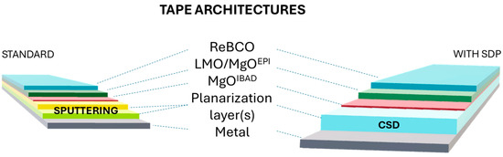
Figure 1.
Schematic representation of the typical CCs architecture.
An alternative to this multi-technique method is represented by solution deposition planarization (SDP), in which the amorphous layer is deposited via chemical solution deposition (CSD) directly on the metallic template (See Figure 1). The obtained layer(s) would serve both as a planarization layer and as a barrier against diffusion, substituting the polishing + oxide sputtering processes. SDP has the overall advantages of reducing substrate polishing costs and minimizing apparatus costs. The principle behind SDP is that, upon coating with a liquid solution, the surface tension of the liquid planarizes the rough surface, resulting in thicker regions over valleys and thinner regions over peaks (Figure 2) [32]. After drying and pyrolysis, the coating shrinks following the original substrate contours, with a decrease in roughness compared to the underlying substrate. By repeating this process a number of times, further reduction in surface roughness, Rrms, can be obtained. More in detail, in order to meet IBAD surface requirements, the number of solution coatings needed is a function of starting substrate roughness, solution shrinkage rate, and the surface tension of the metal compound solution. The main drawback of this technique is that the efficiency of planarization is low, with many coatings required to obtain Rrms < 1 nm. However, many groups have devoted much effort to the implementation of this technique and to demonstrate its applicability to the CC production industry. In the following paragraphs, general considerations of the techniques are given before the systematic review of the literature on the topic.
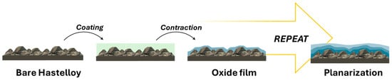
Figure 2.
Schematic representation of the SDP technique.
2. General Considerations
The substrate–In the SDP-related literature, the most widely used substrate is Hastelloy C276, an alloy of Ni, Mo, and Cr currently employed in the coated conductor industry. The templates used in the SDP studies are both polished and unpolished. Unpolished substrates show Rrms of tens of nm (20–50 nm on a scale of 10–50 μm in [1,3,4,5,11,28,33,34,35,36]), whereas polished substrates show Rrms < 10 nm on the same scale [6,37,38,39,40,41,42,43]. The polished substrates are prepared via electropolishing in most of the examples; some works make use of partially polished substrates, showing that it is possible to further decrease the roughness values with SDP [32,38,42,44]. Another possible substrate is SUS304, a stainless steel containing Ni and Cr. Only unpolished SUS304 is employed in the referenced papers [3,35,45,46], with high values of roughness reaching 50 nm on a 10 μm × 10 μm scale. The goal of the research on SDP is to obtain Rrms values below 1 nm, that is the threshold value for IBAD-MgO successful deposition. The main issues related to metallic substrates are surface roughness, of course, that is scale-dependent due to the undulations of the tape, and the diffusion of ions from the upper layers during thermal treatments, which makes the presence of buffer layers necessary. In isolated cases, buffered templates were used to test the SDP technology, such as alternating-ion-beam-assisted, yttrium-doped ZrO2 on stainless steel (ABADYSZ-SS) or Al2O3-buffered Hastelloy. The literature review reveals that SDP was studied both at a laboratory scale and a larger scale.
The coating oxide–SDP makes use of amorphous oxide layers to achieve two goals: avoid diffusion from the substrate and reduce the template roughness. Y2O3 is the most used oxide for SDP due to its compatibility with the metallic template [35]. However, its tendency to recrystallize at temperatures close to those necessary for pyrolysis of the precursor solution leads to some difficulties in developing the optimal heat treatment. Indeed, the treatment temperature is defined by a delicate balance between the decomposition of the organic precursors, whose residues are detrimental to the final film morphology, and oxide recrystallization, which causes grain coarsening and leads to final rougher films. Moreover, its weak bonding energy with MgO can possibly lead to delamination of the CC architecture [42] and mixed oxides such as Y2O3-Al2O3 (in various proportions [11,32,39]) or Y2O3-ZrO2 [44] can be used to avoid the recrystallization during thermal treatment. Al2O3 was found to be a convenient alternative to make up for the high shrinkage percentage of Y2O3 solutions [41]. Other materials studied for this purpose are Gd-doped ZrO2 and 5% Zr-doped CeO2 [6,41,42].
The coating technique–As already mentioned, the SDP effectiveness has already been demonstrated in industrially relevant environments. Apart from a few studies that deal with specific issues and rely on spin-coating, a large part of the reviewed literature uses dip coating for short-length samples (tens of centimetres) or reel-to-reel dip coating for longer samples (tens of metres). The optimization of the deposition speed, so as to promote deposition uniformity, maximize thickness, and so on, was performed in [3]. There is general agreement on the fact that medium deposition speeds offer the best balance between thickness and edge cracking. An isolated yet successful example of SDP with inkjet printing is given in [43], together with the optimization of the inks for different types of substrates. A schematic representation of the three different techniques is shown in Figure 3.
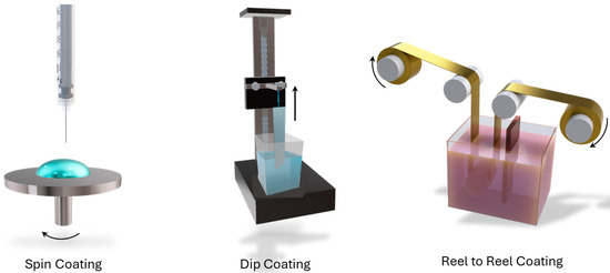
Figure 3.
Schematic representation of the three main deposition techniques employed for SPD: spin coating, dip coating, and reel-to-reel coating.
The chemical technique–Several solution deposition techniques were studied for SDP. Metal–Organic Decomposition (MOD) and its variations are the most common. MOD has the advantage of being well-known from the studies available on chemical deposition of YBCO [15,18,47]. The most widely used precursor (for Y2O3) SDP is yttrium acetate Y(CH3COO)3·4H2O, the source of Y3+ in all low-fluorine and fluorine-free derivatives of MOD YBCO preparation. The thermal decomposition behaviour of this salt is presented in [37], which is essential knowledge when designing the thermal treatment for SDP. It shows two principal mass loss events, one up to 120 °C due to loss of water, and one up to 450 °C related to the decomposition of the acetate via the two-step process.
Y(CH3COO)3·4H2O → Y(CH3COO)3 + 4H2O
2Y(CH3COO)3 + 12O2 → Y2(CO3)3 + 9CO2 + 9H2O
Y2(CO3)3 → Y2O3 +CO2
It goes without saying that the decomposition of a MOD precursor solution is complicated by the presence of the solvents and their evaporation. Y(CH3COO)3 is insoluble in alcohol; therefore, organic acids must be added to the solution. Even when complete dissolution was obtained, these solutions were not stable for long, leading to the precipitation of salts coming from the hydrolysis and trans-esterification reactions. Sometimes, acetylacetonates are used since they are known to be more stable regarding hydrolysis. To improve solution stability, the use of additives is a common strategy. Diethanolamine (HN(CH2CH2OH)2) is by far the most common, but diethylentriamine ((NH2CH2CH2)2NH) was also reported [35]. Additives are molecules whose free electron pairs on the nitrogen atoms and can provide additional coordination to the Y3+ (or other Mn+ metal) atoms with respect to the acetate ligands in the solution, keeping the metal ions from precipitating. The MOD technique applies to the growth of other oxides via the same pathway, starting from different metalorganic precursors such as gadolinium acetate Gd(CH3CO2)3·xH2O, zirconium(IV) acetylacetonate Zr(C5H7O2)4 and cerium acetate Ce(CH3CO2)3·xH2O (for Gd-Zr-O and Zr-doped CeO2). In some cases, mixed precursors, both organic and inorganic, are used, for example, when Al2O3 is grown from Al(NO3)3. Less frequently the sol–gel technique is used, where the precursors used are not carboxylic salts as in MOD but metal alkoxides [35,48]. The main differences with MOD are the decomposition pathway and byproducts of the organic part during pyrolysis. The advantage of this approach is that it does not require any distillation step, which is common in the MOD technique. The prepared solutions are also more stable to hydrolysis with respect to MOD solutions, but they offer no advantage in terms of efficiency. Once the composition of the solution is defined, another parameter to evaluate is the solution concentration. For the goal of planarizing a rough substrate, a thick layer of amorphous material needs to be deposited. Higher solution concentrations lead to thicker films, but, as shown in the following paragraphs, it was experimentally proven that the direct correlation is not only with thickness but also with the increase in surface roughness. Therefore, lower solution concentrations are preferred, with the disadvantage of making the deposition of multilayer necessary to reach the desired surface flatness. The concept of multilayer spans from 4 to 30 layers, depending on the deposition method and related parameters, but still, the repetition of deposition/heat treatment cycles makes the whole SDP process very inefficient. The origin of this resides in the high shrinkage percentage of the deposited films: indeed, a precursor solution with large carboxylate molecules will suffer a severe mass loss after the decomposition of the organic part. Moreover, low molarity solutions will leave, after solvent evaporation, an even lower amount of material on the template surface to fill its natural asperities. It was already mentioned that higher concentrations are not a viable option, even when processing parameters, such as heating ramps, that are known to strongly influence the final film morphology, are carefully optimized. Therefore, multilayers seem to be the only possible choice.
A completely different approach to overcome this problem was successfully proposed in [38] and studied further in [49], named colloid-solution deposition planarization (CSDP), where the first layer of SDP is performed with a Y2O3 particle dispersion. When the particles are of the right dimension, they can drastically reduce the surface roughness of the template with only one coating. Further refinement of the surface is performed with a standard MOD solution. Thus, the total number of coatings is reduced and the efficiency of the technique, expressed as with % defined as , from the few units of the other referenced papers [1,4,5,28,33,34,35,36,37] to more than 20%, also on long-length samples (1 m). A summary of the chemical techniques’ main characteristics is presented in Table 1.

Table 1.
Main characteristics of the SDP chemical techniques.
The thermal treatment–The general thermal treatment for chemical solution deposition processes consists of two steps: decomposition of the organic part and sintering of the oxide. The optimal sintering temperature is a trade-off between the carbon residue and surface smoothness. Carbon residues, detrimental for the growth of the following layers, are eliminated with high-temperature treatments, but low temperatures are required to obtain an amorphous layer. No matter how the precursor solution is prepared, if it contains organic precursors, it will manifest problems related to carbon residues in the film [48], especially when the thermal processing requires low temperatures (T < 600 °C) [50] to avoid crystallization of the oxides; therefore, these two processes are in competition. Moreover, inert atmospheres can be useful to shift the crystallization of the oxide to higher temperatures, but they also cause significant accumulation of carbon in the final film. To complicate matters further, it was shown that the heating ramps and the sintering temperature are also related to final smoothness and IBAD layer texture (see Table 2), edge cracking, that is negligible at a low temperature [49], and delamination strength, that increases at higher sintering temperatures [43]. Again, a delicate balance between positive and negative temperature-induced effects must be found.
3. Review of the Literature
In the following paragraphs, the available literature on SDP is reviewed. To simplify the reading, the literature is classified according to the oxide chosen for planarization, starting from the most common Y2O3. The results are summarized in Table 3.
3.1. Planarization with Y2O3
Wen et al. [37] used the MOD precursor solution with additives to coat laboratory scale samples (1 cm2) of an electropolished Hastelloy substrate, with an initial roughness of 8 nm. The precursor solution concentration varies from 0.05 to 0.4 M. They investigated, with XRD, the effect of the heat treatment temperature, showing that amorphous Y2O3 is obtained at 470, 500, and 530 °C. Partial crystallization of yttria is instead observed at 560 and 590 °C. The effect of temperature on final film roughness for a 3-times spin-coated 0.4 M solution is investigated via AFM, and the result is in accordance with the XRD results, with the lowest roughness obtained at the maximum temperature before crystallization (530 °C). Also, the optimization of the rotation speed during spin coating was performed, evaluating the roughness of the final films, with the identification of 3000 rpm for 30 s as the best option. With regard to the effect of solution concentration and number of coatings, the average roughness values were decreased with an increased number of coatings and with low solution concentrations. The lowest value of 0.65 nm was obtained for 6 layers of 0.1 M solution, deposited at 3000 rpm for 30 s, and treated at 530 °C, with a planarization efficiency of 15%.
In a similar way, MOD Y2O3 without additives was used for the planarization of 50 m Hastelloy substrates in [29]. After 15 SDP coating, the roughness value on the 5 μm × 5 μm scale goes from 50 nm to 1.2 nm (efficiency 6.5%). The subsequent deposition of IBAD-MgO and epi-MgO demonstrated the efficiency of such templates, with MgO XRD analysis throughout the length of the tape showing FWHM values of (110) Δϕ and (200) Δω in the range of 5.5°–6.0° and 3.0°–3.5°, respectively. In addition, the effect of the thickness of the epi-MgO layer on its surface roughness was presented, and a direct relationship between thickness and roughness is shown. On a 50 nm epi-MgO film, an excellent LMO film was sputtered, with the FWHM values of (110) Δϕ and (200) Δω being 3.7° and 6.8°, respectively. It should be pointed out that after MgO and LMO deposition, partial recrystallization of yttria occurs, but it does not seem to influence the quality of the final LMO layer. Such templates were used in [34], for the deposition of YBCO via MOCVD via reel-to-reel dip coating, with a resulting Jc = 1.8 MA/cm2.
In [5] SPD is applied to long-length IBAD templates (about 5 m long) using MOD-derived amorphous Y2O3 deposited with a continuous tape loop coater. Diethanolamine was used in the precursor solution to enhance its stability. The effect of two parameters on the final film roughness was analyzed, namely the precursor solution concentration (0.08 M and 0.4 M) and the number of coatings (1–30). They found out that coating with a combination of the two solutions led to the best results in terms of roughness reduction, from the starting Rrms = 21 nm (5 μm × 5 μm scale) to the final Rrms = 0.5 nm (5 μm × 5 μm scale) after 15 coatings with the 0.4 M solution and 15 coatings with the 0.08 M solution, with a final planarization efficiency of 3% (Figure 4a,b). This template was used for the deposition of IBAD-MgO, that displayed goon in-plane and out-of-plane texture (FWHMo-o-p2°, FWHMi-p4°). YBCO deposition was carried out via both PLD and RCE. In the first case, with the aid of a SrTiO3 buffer layer, a Jc = 2.85 MA/cm2 is obtained; in the second case, without any additional buffer layer, a Jc = 4 MA/cm2 is obtained. Higher solution concentrations (0.1 up to 0.6 M) were studied in [1]. The results obtained with low molarities are comparable to [5], whereas the use of 0.6 M does not give any advantage in terms of a possible reduction in the number of coatings, while it causes the formation of cracks randomly distributed on the surface of the amorphous Y2O3 layer. Comparable results are obtained by Nie et al. in [4].
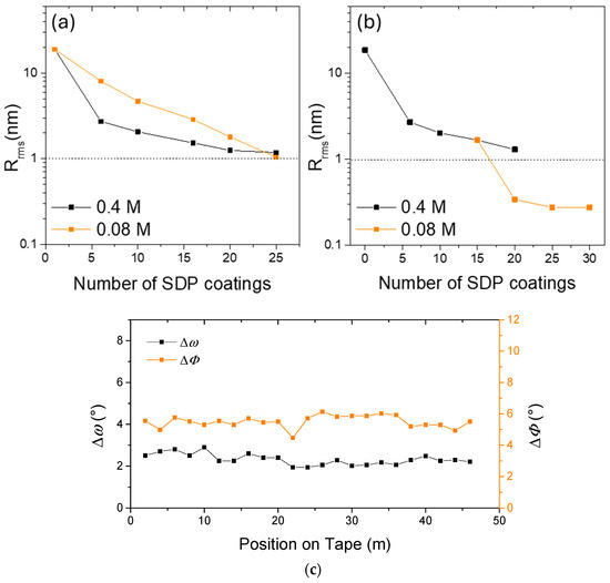
Figure 4.
(a) Rrms over a 5 μm × 5 μm area, as a function of the number of SDP coatings for 0.08 M and 0.4 M solutions; (b) Rrms for the 0.4 M solution coatings followed by coatings with a 0.08 M solution on a 5 μm × 5 μm area. Data from [5] were used. (c) ΔΦ and Δω distributions of MgO templates along the 50 m Hastelloy tape. Data from [28] were used.
The same system (long-length Hastelloy, MOD Y2O3 + additives, and the continuous dip coating) was studied in [3]. In this case, the effect of deposition speed on the single coating uniformity of the solution was analyzed by means of optical microscopy focused on the edges of the tape. The speed was varied between 30 and 70 cm/min, and the best uniformity was obtained at the intermediate speed of 60 cm/min. Using this reference speed, the number of coatings for optimal planarization was studied, the value of Rrms = 0.573 nm (5 μm × 5 μm scale) was obtained, and homogeneous values of Rrms were measured along the whole length of the tape (Figure 5a). This value, together with an initial Rrms = 11.74 nm, results in an 11% efficiency. On such samples, IBAD-MgO and LMO were then deposited. Surprisingly, the samples with lower Rrms did not lead to the best texture of the superior epi-MgO and LMO layers. Indeed, the lowest values of FWHMo-o-p = 5.83° were obtained for the 16-coating sample. This phenomenon is in contrast with what was observed in [5], where Rrms and FWHMo-o-p showed the same behaviour vs. the number of coatings. This template was used for YBCO deposition via MOD. The superconducting critical currents at 77 K in self-field were in the range of 80–180 A (Figure 5b).
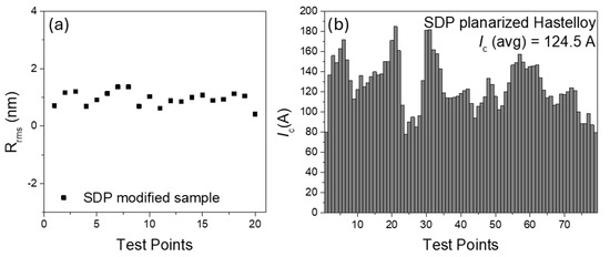
Figure 5.
(a) The Rrms of 10 m length with 16 coating layers of SDP on Hastelloy over a 5 μm × 5 μm area; (b) critical currents at 77 K in self-field for the same sample. Data from [3].
In [34], the previously discussed system is directly compared with other planarization methods (i.e., electropolishing and mechanical polishing) using the same experimental setup. No information on the solution concentration is given, but the precursor salts and additives are the same. The solvent is a mix of ethanol and water, instead of methanol. This difference, nor the unknown solution concentration seem to lead to significantly different results, with the Rrms that decreases to 5% of the initial value (1 nm) after 16 coatings, a value comparable to those previously mentioned, with an overall efficiency of 6%. The conclusion of this work is that all three methods were demonstrated to be good processing techniques for planarization, with the main advantage of SPD of providing simultaneously a nucleation layer for MgO.
SDP with MOD Y2O3 was used to planarize also the intermediate layers in a stack with the following architecture Y2O3CSD/MgOIBAD/YBCO(1)/Ag/Y2O3CSD/MgOIBAD/YBCO(2)/Ag [36]. The idea behind this model is that of increasing the Ic of the coated conductor by stacking two YBCO films, with the final current density being the sum of the individual ones. The advantage of using Y2O3 SDP on top of the intermediate layer of Ag is that it resets the crystalline structure of the system before another YBCO deposition, thus making it independent of any defect present in the previous one and from its roughness (see Figure 6). The planarization process was successful both on the bare Hastelloy (efficiency 6.4%) and on the intermediate Ag layer, with the obtained Rrms < 1 nm. The final stacks of well-textured YBCO layers showed a total Ic of 725 A/cm on a 7 cm long sample.
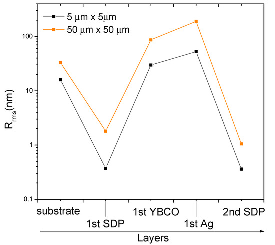
Figure 6.
Rrms of the layers surfaces in a Y2O3CSD/MgOIBAD/YBCO(1)/Ag/Y2O3CSD stack. Data from [45].
The possibility of using SPD with Y2O3 films on stainless steel (SS) was studied in [3,45]. In [3], the SUS304 substrate was used to perform the same study carried out by the group for Hastelloy presented before. For SUS304, the optimal dip coating speed was found to be 50 cm/min, and the number of coatings for a final film roughness Rrms = 0.9 nm was 12. The initial substrate roughness was Rrms = 20.93 nm, which gave a final efficiency of 8%. On such samples, the full SUS304/Y2O3CSD/MgOIBAD/MgOEPI/LMO/YBCOMOD was realized, and the resulting transport properties of the tape are promising (Figure 7a). Vilardell et al. [45], instead, used SS substrates (both polished and unpolished), and inkjet printing as a deposition technique. The preparation of the ink required an adjustment of the standard MOD precursor solution, not only through the use of additives, but also of a UV varnish. The ink’s properties were thoroughly analyzed and optimized for deposition on both unpolished and polished samples, and for long-length unpolished samples (100 m). With inkjet printing, only one step of coating is required to reduce the roughness enough to deposit YSZABAD with a 66% efficiency. On short samples (approx. 1 m) it was possible to prepare the full SS/Y2O3CSD/YSZABAD/CeO2 PLD/YBCOPLD stack and measure its properties. The optimal texture was obtained for the YSZ layer, but rather low values of Ic were obtained on both polished and unpolished substrates (Figure 7b).
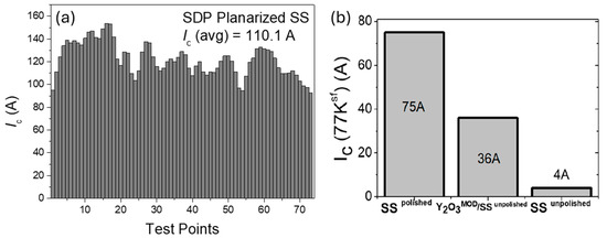
Figure 7.
(a) Critical currents at 77 K in self-field for the SUS304/Y2O3CSD/MgOIBAD/MgOEPI/LMO/YBCOMOD sample, data from [3]; (b) Critical currents at 77 K in self-field for the SS/Y2O3CSD/YSZABAD/CeO2PLD/YBCOPLD sample, reproduced with permission from [35].
The use of yttrium acetate precursor in the standard MOD procedure requires, as already mentioned, the use of additives to avoid the precipitation of unwanted byproducts of the hydrolysis in the solution. Another group [35] proposed a mixed alkoxide precursor solution as an alternative, in which the metal ions from different precursors are kept in the solution using chelating agents (Polyethylenglycole, diethylentriamine). Thermogravimetric analysis of such solutions is provided. The SDP was carried out on both Hastelloy and SUS304 substrates with good results in terms of final film roughness. Highly aligned IBAD-MgO layers were successfully grown on these samples, which resulted in high Ic GdBCO films (300–420 A/cm). The planarization efficiencies are slightly above those of standard MOD (4.5% on Hastelloy and 6.5% on SUS304). However, information regarding the length of the deposited samples is lacking, as well as further studies on the applicability of this technique for scale-up.
Another different but more promising approach was used in [38,49] where a colloidal solution of Y2O3 nanoparticles was used to planarize laboratory scale samples of Hastelloy, also in combination with the MOD technique. The idea was to make up for the lack of efficiency of SDP with standard MOD, that requires many coatings steps to obtain the desired Rrms values. The use of a colloidal solution is considered a faster planarization process, since the particles fill the macroscopic defects of the substrate in one single coating, thanks to the lower shrinkage percentage of the colloid deposition layer. Afterwards, another few steps with MOD lead to further refinement of the surface in [38], with the reduction of Rrms of mechanically polished Hastelloy from 4.0 nm to 0.3 (Figure 8) with an efficiency of 24%. Moreover, the RHEED pattern of IBAD-MgO on Hastelloy substrate with such coating indicates that the MgO layer was monocrystalline, confirming the efficiency of this technique. This work on colloidal solutions was taken further by Wang et al. [49], who investigated the effect of various parameters, such as Y2O3 concentration, dip coating pulling rate, viscosity, and heat treatment temperature on the edge cracking phenomenon on long-length Hastelloy. They also provide TGA analysis of the Y2O3 colloidal solution, that identifies the temperature where the unwanted crystallization of Y2O3 starts. The planarization efficiencies for the samples prepared with Y2O3 dispersions are, also in this case, far higher than for standard MOD (22.5%). This makes the technique very promising for low-cost production of HTS-CCs.
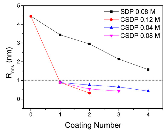
Figure 8.
Surface roughness of Hastelloy substrate after using colloidal SDP and traditional SDP. Data from [39].
3.2. Planarization with Y2O3 + MxOy
One of the main issues connected to the use of pure Y2O3 in SDP is related to its recrystallization during thermal treatment, which can cause an increase in surface roughness. For this purpose, mixed oxides can be used as an alternative [33]. Kim et al. [44] used a mix of Y2O3 and ZrO2 with the MOD + additives technique. Two solution concentrations were studied (0.1 M and 0.2 M), and the substrate surface roughness was significantly reduced (from 50 nm to 3.8 nm) after 20 dip coatings with the 0.1 M solution. Good in-plane and out-of-plane textures of the IBAD-MgO and LMO layers are observed, and the final GbBCO film shows a critical current of Ic = 400 A/cm (77k, self-field).
Xue and co-workers, instead, focused on the Y2O3-Al2O3 (YAlO) composite for SDP. In [11,32], they prepared both the templates and the full YBCO-CC stack using SDP. The precursor solution was prepared with mixed organic/inorganic precursors, and their decomposition behaviour was analyzed. The Y:Al ratio effect on the surface of the SDP layer and on the texture of the MgO layer was analyzed, and the optimal value was found to be 9:1. The efficiency of planarization in this case is 4%. During the deposition of the LMO layer and YBCO layer, partial recrystallization of Y2O3 is visible, but optimal properties are obtained for the complete YBCO-CC with Jc (77 K, sf) of 3.2 MA/cm2.
More complex compositions were studied by Qiao et al. [39], the details of which were not, unfortunately, disclosed. The solutions were made by dissolving organic yttrium, aluminium, and other metal precursors into a solvent with additives, which adjusted the viscosity of the solution. The efficiency of planarization for this method is high, 19%, and the final Y2O3 film roughness is comparable to that of the electropolished Hastelloy. On short planarized samples, the full stack MgOIBAD/MgOEPI/LMO/YBCOMOCVD was deposited, and an Ic of 140 A on a 0.4 μm-thick YBCO was measured, corresponding to a Jc of 3.5 MA/cm2. Most importantly, in this case, the technology was also transferred to long-length tapes (20 m) with a uniform Ic of 160 A on 1 μm-thick YBCO (Figure 9).
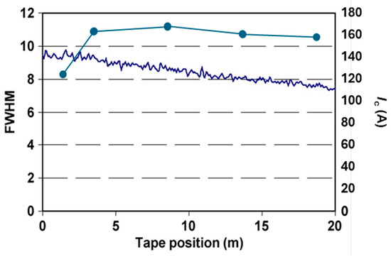
Figure 9.
Texture of LMO (left axis) and Ic (right axis) along a long-length of Y2O3-planarized substrate, data from [47].
Matias et al. also attempted to use mixed oxides for SDP, namely Y2O3 + 10% Al2O3 [51]. On such a sample, the final roughness after 15 coating was excellent (efficiency 6%) and the typical FWHM for the MgO layer on top was 4°–5° in-plane and 1.5° out-of-plane. Reactive co-evaporation of YBCO lead to a 1 μm sample with Jc of 4 MA/cm2 (75K, self-field). The magnetic field dependence of Jc for this sample is comparable to the state-of-the-art undoped YBCO, as well as its angular dependence, with the correlated peak parallel to the ab-planes, and a smaller feature at θ = 0 like other undoped films. When 5 μm YBCO is deposited on such a template, an Ic = 600 A/cm is obtained.
3.3. Planarization with Gd-Zr-O
In a series of dedicated works [6,41,42]. Chu et al. thoroughly analyzed the possibility of applying SPD to Gd-doped ZrO2. This material, having a high melting point, has good barrier performance on IBAD substrates when deposited via sputtering, and it can also serve as the seed layer for MgO. The investigation in [42] started with the thermogravimetric analysis of the MOD precursor solution to identify the right temperature for the heat treatment. Consequently, the effect of the molarity of the solution and the heating ramp rates’ effect on the final film roughness was evaluated, and the combination of 0.1 M and 5 °C/min led to the lowest value of Rrms = 0.4 nm. In the following paper [41], the effect of SDP on two types of metallic templates with different types of defects was studied. More specifically, grain boundaries and particle segregation are present on Hastelloy electro-polished tapes, while rolling marks are mainly visible on the rolled tapes. With SDP, it was possible to planarize the mirror-rolled Hastelloy to reach Rrms = 5 nm on 50 μm × 50 μm with an efficiency of 5%. The IBAD-MgO layer deposited on top of the template displayed a sharp texture, and it was enabled to achieve Jc = 4.17 MA/cm2 (at 77 K, self-field) in the YBCO layer. In [6], a study on the optimization of the temperature for Gd-Zr-O deposition is given. Like Y2O3, the temperature choice must balance the grain coarsening phenomenon that occurs at high temperatures and the minimization of the carbon residue that increases at low temperatures, which reduces compatibility with the IBAD-MgO layer. Furthermore, the effect of the thickness of the Gd-Zr-O layer on the IBAD-MgO texture was analyzed, changing the precursor solution concentration. It was shown that higher concentrations lead to an IBAD-MgO layer with no texture or weak texture (see Table 2). In conclusion, the TEM cross-section observation shows that the 130 nm-thick Gd-Zr-O monolayer from the 0.8 M solution, under optimal heat-treatment.
Table 2.
Summary of the results presented in [6].
Table 2.
Summary of the results presented in [6].
| Molarity of Soln. [M] | Tsintering [°C] | Heating Ramps [°C/min] | Rrms [nm] | IBAD-MgO Texture |
|---|---|---|---|---|
| 0.8 | 725 | 5 | 0.74 | Strong |
| 0.8 | 625 | 5 | 0.58 | n.d. |
| 0.8 | 425 | 5 | 0.33 | n.d. |
| 0.2 | 425 | >100 | 0.41 | Weak |
| 0.2 | 325 | >100 | 0.31 | Weak |
| 0.2 | 275 | >100 | 0.29 | Weak |
Conditions (Figure 10), can serve as the planarization and seed layer for the IBAD-MgO process, even though the final Jc of the YBCO films is low (1–2 MA/cm2). Optimization of the whole technique is, therefore, required to take full advantage of its promising efficiency values (26%). A summary of the results presented in this series of papers is given in Table 2.
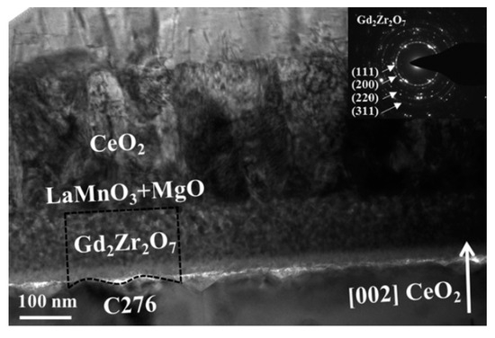
Figure 10.
Low-magnification cross-sectional TEM images of a Hastelloy/Gd-Zr-OCSD/MgOIBAD/LMO/CeO2PLD/YBCOPLD stack and electron diffraction (SAED) patterns of the Gd2Zr2O7 corresponding selected area (inset) represented with permission from [6].
In addition, Nakaoka et al. [43] studied Gd-Zr-O as the planarization layer for roughly electropolished Hastelloy. They obtained a reduction of Rrms down to 2 nm with 4–5 dip coatings of a 0.15 M MOD solution. In these conditions, the planarization efficiency reached 9%. Then, IBAD-MgO, LaMnO3, CeO2, and the YBCO layer were deposited, the last one via the trifluoroacetate (TFA)-MOD method. Notwithstanding the not-so-low roughness of the chemical oxide layer, the SDP method with Gd-Zr-O proved to work as a planarization layer and diffusion barrier layer. Most importantly, the delamination strength was also evaluated as a function of the sintering temperature, and it was shown that high delamination strength was obtained on those samples prepared at T > 550 °C.
3.4. Planarization with Al2O3
Alumina was identified as a possible alternative to Y2O3 to make up for the yttria solution’s high shrinkage percentage. Indeed, Al2O3 can act as a planarization layer with a lower number of coatings, improving the efficiency of the SDP technique. Paranthaman et al. developed an SDP coating with Al2O3 [40,51] using the MOD technique on polished Hastelloy. The samples were deposited via spin coating to obtain a 10–15 nm thick film in a single coat. Multiple depositions and heat treatments were performed, and a final roughness of 2.5 nm is obtained on a 2 μm 2 μm scale, with an overall efficiency of 9%. After that, a Y2O3 nucleation layer followed by MgO (IBAD + Epi), LMO, and YBCO was deposited. The stack shows a self-field Jc of 3.04 MA/cm2 at 77 K with excellent in-field Jc properties, which were induced by the presence of BZO pinning centres. The efficiency of Al2O3 as a barrier against diffusion is proven by TEM imaging since the metal elements Ni, Mn, and Cr can only be found below the Al2O3 layer. However, the need for a sputtered layer of Y2O3 makes the use of CSD less advantageous than other proposed methodologies.
3.5. Planarization with 5% Zr-CeO2
Vlad et al. in [46] used 5% Zr-CeO2 (CZO) for the planarization of ABADYSZ-SS substrate templates. In this case, the starting roughness of the template is low (1.8 nm), but the flat area fraction, defined as a deviation of less than 1.8 nm of the mean surface roughness value, is only 49%. After the deposition of a CZO layer, the overall Rrms was increased up to 3 nm, but the flatness obtained was 75%. The increase in roughness is probably due to the tendency of CZO to form a terraced surface. However, YBCO was successfully grown on top of CZO, with only a limited interfacial reaction, leading to the formation of Ba(Ce,Zr)O3. Transport properties of the SS/YSZABAD/CZOCSD/YBCOCSD coated conductor were analyzed, and, despite a pronounced Jc decrease at low fields, the CC performed as well as the same sample grown on a single crystal. This behaviour at μ0H < 1.5 T is due to the higher granularity of the sample, which reflects the granularity of the substrate. These works show the possibility of eliminating the IBAD-MgO layer and additional buffers (epi-MgO, LMO…) using chemical techniques for both the CZO and the YBCO layer. In [21], these substrates are used for the growth of YBCO via the MOD technique and inkjet printing. The final CC shows Jc(77 K, sf) = 1 MA/cm2, a very porous microstructure, and the presence of secondary BaO and Y2Cu2O5 phases, as shown by STEM images (See Figure 11).
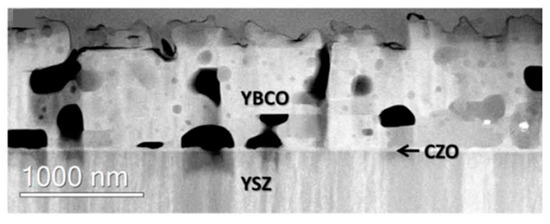
Figure 11.
STEM cross-section image of the CC where the residual porosity is identified. Reproduced with permission from [21].
4. Conclusions and Prospects
SDP was proven to be a cost-effective way of reducing surface roughness in metallic flexible substrates. If we consider its application to HTS-CCs, it becomes clear how it can simplify the first stages of CC preparation by fulfilling both the task of planarization and protection from ion diffusion. The necessity of repeating the coating-drying-pyrolysis step several times does not seem to be a limiting factor since the cost, in terms of time and equipment, is probably still lower than the electropolishing + sputtering apparatus. Moreover, compared to electropolishing, SDP does not require the use of large quantities of concentrated acid solutions, with all the related issues (safety hazard, disposal…). If we compare the results presented in this review with those obtained for systems in which the standard sputtering planarization is used (Table 4), it is clear how they are perfectly comparable. However, the efficiency of the planarization process is still low, and even though some strategies have been proposed to overcome this problem, this remains the main objective of future research in this field. The most obvious idea is to start from a partially polished substrate, either mechanically or electropolished. Thus, the sputtering step is eliminated, and the number of coatings needed to reach Rrms < 1 can be lowered. On the other hand, the possibility of significantly lowering the SDP layers was demonstrated starting from the Y2O3 dispersion proposed in [39,50]; that is a strategy worth exploring further, not only with Y2O3 but also with other compatible materials less prone to shrinkage during sintering. Also, the use of technologically advanced deposition techniques, such as inkjet printing, can prove to be a successful way of integrating SDP in the CC production process, as preliminarily demonstrated in [21,46], due to the possibility to closely control the amount of deposited material and to tune the ink’s properties according to need. In the attempt to develop a new SDP process, these mentioned variations could represent a good starting point. With regard to the coating oxide, Al2O3, Gd-Zr-O, and mixed Y2O3-Al2O3 show higher efficiencies due to lower shrinkage rate, and their precursor solutions are more stable than those of Y2O3. The possibility of using more viscous solutions for deposition techniques, such as dip coating using additives with low boiling points, could be worth investigating so as to deposit more solution in a single coating on the substrate without changing the solution concentration, thus obtaining thicker films that were proven to be highly efficient in reducing surface roughness. Further refinement of the surface can be carried out with lower molarity solutions. The thermal treatment temperature should be optimized to minimize both carbon residue and oxide crystallization; heating ramps should allow for a slow removal of the solvents/evolution of gasses that would not damage the film morphology; also, cooling ramps should be controlled so as to control strain accumulation due to different thermal expansion coefficients between oxide and metal, and to avoid the formation of cracks. With respect to what has already been achieved, there is probably still room for improvement.
All in all, with so many parameters to possibly optimize, SDP holds the promise of being a beneficial integration component in the CC production process. It cannot be considered a game changer, but it can be beneficial in terms of cost reduction and production speed. Indeed, should it substitute both the polishing and sputtering steps, the capital cost and operating cost for HTS CC planarization would be significantly reduced. However, this goal can only be achieved if it really becomes competitive with the standard procedure, that is to say if the efficiency of the technique is significantly increased.
Table 3.
Summary of the results presented in the literature.
Table 3.
Summary of the results presented in the literature.
| Ref | Oxide | Substrate | Precursor | Deposition | Layers (Tot Thickness) | Roughness R (Scale) ) | Final Structure | Efficiency | Length | Jc/Ic (77K, sf) |
|---|---|---|---|---|---|---|---|---|---|---|
| [5] | Y2O3 | Hastelloy (Unpolished) | Metal–Organic + additives | Continuous Dip coating | 30 (~1 μm) | <1 nm (5 μm × 5 μm) (97.6%) | Hastelloy/Y2O3CSD/MgOIBAD/YBCOPLD,RCS | 3% | 5 m | Jc = 2.85–4 MA/cm2 |
| [45] | Y2O3 | YZSABAD/SS (unpolished) | Metal–organic + additives (TEA) + UV Varnish | R2R inkjet | 1 (90–100 nm) | 5.4 nm (5 μm × 5 μm) (66%) | SS/Y2O3CSD/YSZABAD/CeO2PLD/YBCOPLD | 66% | Ic = 36 A | |
| [3] | Y2O3 | Hastelloy (unpolished) | Metal–organic + additives | Continuous Dip coating | 16 | 0.788 nm (5 μm × 5 μm) (95%) | Hastelloy/Y2O3CSD/MgOIBAD/MgOEPI/LMO/YBCOMOD | 11% | 10 m | Ic = 80–180 A |
| SUS 304 (unpolished) | 12 | 0.903 nm (5 μm × 5 μm) (95.7%) | SUS304/Y2O3CSD/MgOIBAD/MgOEPI/LMO/YBCOMOD | 8% | Ic = 100–150 A | |||||
| [28,33] | Y2O3 | Hastelloy (unpolished) | MOD | Continuous Dip coating | 15 (840 nm) | 1.2 nm (5 μm × 5 μm) (97%) | Hastelloy/Y2O3CSD/MgOIBAD/MgOEPI/LMO | 6.5% | 50 m | Jc = 1.8 MA/cm2 |
| [1] | Y2O3 | Hastelloy (unpolished) | MOD + additives | R2R dip coating | 30 (0.5–1.2 μm) | 1.2 nm (5 μm × 5 μm) (95.9%) | Hastelloy/Y2O3CSD | 3% | n.d | n.d |
| [37] | Y2O3 | Hastelloy (e-polished) | MOD + additives | Spin coating | 6 | 0.65 nm (5 μm × 5 μm) 92% | Hastelloy/Y2O3CSD | 15% | Lab. scale | nd |
| [34] | Y2O3 | Hastelloy (unpolished) | MOD + additives | R2R dip coating | 16 (10 nm) | 1.2 nm (5 μm × 5 μm) 94% | Hastelloy/Y2O3CSD/MgOIBAD/MgOEPI | 6% | n.d | n.d |
| [38] | Y2O3 | Hastelloy (mechanically polished) | Y2O3 dispersion (1° step) MOD + additives (2° step) | Spin coating | 2 (1° + 2° step) | 0.3 nm (5 μm × 5 μm) 95% | Hatelloy/Y2O3CSD/MgOIBAD | 24% | Lab. scale | n.d |
| [49] | Y2O3 | Hastelloy | Y2O3 dispersion | Dip coating | 4 | 1.28 nm (5 μm × 5 μm) 90% | Hastelloy/Y2O3CSD | 22.5% | 1 m | nd |
| [35] | Y2O3 | Hastelloy (unpolished) | Mixed Alkoxides + chelating agents | Dip coating | 20 (1300 nm) | 5 (10 μm × 10 μm) 90% | Hastelloy/Y2O3CSD/MgOIBAD/LMO/GdBCO | 4.5% | n.d. | Ic = 420 A/cm |
| SUS 304 (unpolished) | 15 (150 nm) | 0.36 (10 μm × 10 μm) 98.2% | SUS304/Y2O3CSD/MgOIBAD/LMO/GdBCO | 6.5% | n.d. | Ic = 300 A/cm | ||||
| [36] | Y2O3 | Hastelloy (unpolished) | MOD + additives | Continuous dip coating | 15 (1 μm) | 0.7 nm (5 μm × 5 μm) 96.5% | Hastelloy/Y2O3CSD/MgOIBAD/ YBCO(1)/Ag/Y2O3CSD/MgOIBAD/YBCO(2)/Ag | 6.4% | 5 m | Ic = 725 A/cm (YBCO1 + 2) |
| [4] | Y2O3 | Hastelloy (unpolished) | MOD | Continuous dip coating | 24 (730 nm) | 1.5 nm (5 μm × 5 μm) 96.4% | Hastelloy/Y2O3CSD/MgOIBAD/MgOEPI/LMO/YBCO | 4% | n.d. | Jc = 2.5 MA/cm2 |
| [44] | Y2O3-ZrO2 | Hastelloy | MOD + additives | Dip coating | 20 (440 nm) | 3.8 (10 μm × 10 μm) 80% | Hastelloy/YZrOCSD/MgOIBAD/LMO/GdBCO | 4% | n.d | Ic = 400 A/cm |
| [11] | Y2O3+ Al2O3 (YAlO) | Hastelloy (unpolished) | MOD + additives | Continuous dip coating | nd | 0.2 (5 μm × 5 μm) 99.6% | Hastelloy/YAlOCSD/MgOIBAD/LMO | n.d. | n.d | n.d. |
| [39] | Y2O3+ Al2O3 + MOx | Hastelloy (polished) | Mixed precursors + additives | Continuous Dip coating | 4 (n.d.) | 0.6 (5 μm × 5 μm) 76% | Hastelloy/YAlOCSD/MgOIBAD/MgOEPI/LMO/YBCO | 19% | 20 m | Ic = 160 A |
| [32] | Y2O3+ Al2O3 (YAlO) | Hastelloy | Mixed precursors | Continuous Dip coating | 24 (730 nm) | 1.6–1.8 nm (5 μm × 5 μm) 96.8% | Hastelloy/YAlOCSD/MgOIBAD/MgOEPI/LMO/YBCO | 4% | n.d. | Jc = 3.2 MA/cm2 |
| [52] | Y2O3+ Al2O3 | Hastelloy unpolished | N.d | N.d | 15 (1.2 um) | 1.5 (5 μm × 5 μm) 95.2% | Hastelloy/YAlOCSD/MgOIBAD/MgOEPI/YBCO | 6% | n.d. | Ic = 600 A/cm |
| [40] | Al2O3 | Hastelloy (polished) | MOD | Spin Coating | 8 (~50 nm) | 2.5 (2 μm × 2 μm) 74% | Hastelloy/Al2O3CSD/Y2O3/MgOIBAD/MgOEPI/LMO/YBCO | 9% | 10 cm | Jc = 3.04 MA/cm2 |
| [41] | Gd-Zr-O | Hastelloy (E-polished) | MOD | Dip coating | 9 | 4.2 (50 μm × 50 μm) 48% | Hastelloy/Gd-Zr-O/MgOIBAD/CeO2/YBCO | 5% | n.d. | n.d. |
| Hastelloy (Mirror-rolled) | 9 (~300) nm | 5 (50 μm × 50 μm) 83% | 9% | nd | Jc = 4.17 MA/cm2 | |||||
| [6] | Gd-Zr-O | Hastelloy (e-polished) | MOD | Dip coating | 1 (130 nm) | 0.74 (1 μm × 1 μm) 26% | Hastelloy/Gd-Zr-OCSD/MgOIBAD/LMO/CeO2PLD/YBCOPLD | 26% | 20 cm | Jc = 1–2 MA/cm2 |
| [42] | Y2O3 Gd-Zr-O | Al2O3-coated Hastelloy | MOD | Dip coating | 1 (30–50 nm) | 0.5 (1 μm × 1 μm) | Hastelloy/Gd-Zr-O/MgOIBAD/CeO2/YBCO | n.d. | 20 cm | Jc = 1.65 MA/cm2 |
| [43] | Gd-Zr-O | Hastelloy e-polished | MOD | Dip coating | 4–5 | 2.5 - 40% | Hastelloy/Gd-Zr-OCSD/MgOIBAD/LMO/CeO2PLD/YBCOCSD | 9% | n.d. | Jc = 2.5 MA/cm2 |
| [46] | CZO | YSZABADSS | MOD | Spin coating | 1 (30 nm) | 3 (5 μm × 5 μm) | SS/YSZABAD/CZOCSD/YBCOCSD | Jc = 1.8 MA/cm2 |
Table 4.
Relevant characteristics of systems planarized via sputtering.
Table 4.
Relevant characteristics of systems planarized via sputtering.
| Ref | Group | Complete Buffer Structure | IBAD Substrate Rrms | Jc ReBCO |
|---|---|---|---|---|
| [53] | SuperPower | LMO/MgOEPI/MgOIBAD/Y2O3SPUTTERING/Al2O3SPUTTERING | 1.5–2 nm | 3.06 MA/cm2 |
| [52,54] | Los Alamos National Lab. | LMO/MgOEPI/MgOIBAD/Y2O3SPUTTERING/Al2O3SPUTTERING | 4–5 nm | 4.25 MA/cm2 |
| LMO/MgOIBAD/Y2O3SPUTTERING/Al2O3SPUTTERING | 6–8 nm | 4.1 MA/cm2 | ||
| LMO/MgOEPI/MgOIBAD/YAlOSPUTTERING | 4.5–5.5 nm | 2.9 MA/cm2 | ||
| [55] | Fujikura | CeO2/LMO/MgOIBAD/Y2O3SPUTTERING/Al2O3SPUTTERING | 2.5 nm | 1.36 MA/cm2 |
| [56] | SuNAM | LMO/MgOEPI/MgOIBAD/Y2O3SPUTTERING/Al2O3SPUTTERING | 1.6 nm | 4.8 MA/cm2 |
| [57] | Shangai Univesity SJTU | CeO2/MgOEPI/MgOIBAD/Y2O3SPUTTERING/Al2O3SPUTTERING | 1.5–2 nm | 4 MA/cm2 |
| [58] | Superconductivity Research Laboratory, ISTEC | CeO2/MgOEPI/MgOIBAD/Y2O3SPUTTERING/Al2O3SPUTTERING | 2 nm | 2.6 MA/cm2 |
Author Contributions
Conceptualization, L.P.; writing-original draft preparation, L.P.; writing-reviewing and editing, L.P. and G.C. All authors have read and agreed to the published version of the manuscript.
Funding
This research received no external funding.
Institutional Review Board Statement
Not applicable.
Informed Consent Statement
Not applicable.
Data Availability Statement
Not applicable.
Conflicts of Interest
The authors declare no conflicts of interest.
References
- Kang, B.M.; Ko, R.K.; Kim, D.H.; Ha, D.W.; Park, S.S. Planarization of flexible tape substrate by solution coating process. Prog. Supercond. Cryog. 2011, 13, 18–21. [Google Scholar] [CrossRef]
- Sheehan, C.; Jung, Y.; Holesinger, T.; Feldmann, D.M.; Edney, C.; Ihlefeld, J.F.; Clem, P.G.; Matias, V. Solution deposition planarization of long-length flexible substrates. Appl. Phys. Lett. 2011, 98, 071907. [Google Scholar] [CrossRef]
- Du, W.; Bai, Y.; Wang, J.; Fang, F. Effective surface modification by chemical solution deposition for flexible metal substrates. Mater. Res. Express 2017, 4, 035033. [Google Scholar] [CrossRef]
- Nie, Q.; Jiang, J.; Qu, H.; Cheng, Y.; Wang, S.; Wang, J.; Wang, J.; Yang, B.; Qing, Z.; Xue, Y. Biaxially textured MgO buffer layer on flexible metal template for coated conductor. J. Mater. Sci. Mater. Electron. 2022, 33, 16678–16687. [Google Scholar] [CrossRef]
- Sheehan, C.; Jung, Y.; Holesinger, T.; Matias, V. Solution deposition planarization for ion beam texturing of long-length flexible substrates. In Proceedings of the MRS Fall Technical Conference, Boston, MA, USA, 2 December 2010. [Google Scholar]
- Chu, J.; Zhao, Y.; Jiang, G.; Wu, W.; Zhang, Z.; Hong, Z.; Jin, Z. Surface engineering of the flexible metallic substrate by SDP-Gd-Zr-O layer for IBAD-MgO templates. J. Am. Ceram. Soc. 2019, 102, 2415–2425. [Google Scholar] [CrossRef]
- Xu, Z.; Yuan, P.; Ma, Y.; Cai, C. High-performance FeSe0. 5Te0. 5 thin films fabricated on less-well-textured flexible coated conductor templates. Supercond. Sci. Technol. 2017, 30, 035003. [Google Scholar] [CrossRef]
- Huang, J.; Chen, L.; Jian, J.; Khatkhatay, F.; Jacob, C.; Wang, H. A simplified superconducting coated conductor design with Fe-based superconductors on glass and flexible metallic substrates. J. Alloys Compd. 2015, 647, 380–385. [Google Scholar] [CrossRef]
- Thomas, A.A.; Shipulin, I.A.; Holleis, S.; Eisterer, M.; Nielsch, K.; Hühne, R. Comparative study of Fe(Se, Te) thin films on flexible coated conductor templates and single-crystal substrates. Supercond. Sci. Technol. 2021, 34, 115013. [Google Scholar] [CrossRef]
- Ko, R.; Kang, B.; Kim, D.; Ha, D.; Park, C.; Yoon, S.; Kim, Y. Effect of Solution Concentration on the Surface Properties of Y2O3 Solution-Coated Film on Flexible Metal Substrate. Met. Mater. Int. 2013, 19, 1343–1345. [Google Scholar] [CrossRef]
- Xue, Y.; Zhang, Y.H.; Zhang, F.; Zhao, R.P.; Wang, H.; Xiong, J.; Tao, B.W. Growth of simplified buffer template on flexible metallic substrates for YBa2Cu3O7-δ coated conductors. J. Alloys Compd. 2016, 673, 47–53. [Google Scholar] [CrossRef]
- Obradors, X.; Puig, T.; Ricart, S.; Palau, A.; Coll, M.; Gutiérrez, J.; Farjas, J.; Bartolomé, E. Progress in superconducting REBa2Cu3O7 (RE = rare earth) coated conductors derived from fluorinated solutions. Supercond. Sci. Technol. 2024, 37, 053001. [Google Scholar] [CrossRef]
- MacManus-Driscoll, J.L.; Wimbush, S.C. Processing and application of high-temperature superconducting coated conductors. Nat. Rev. Mater. 2021, 6, 587–604. [Google Scholar] [CrossRef]
- Ma, Y.; Xiao, L. Second generation YBCO coated conductors: A review. Chin. Sci. Bull. 2004, 49, 2435–2439. [Google Scholar] [CrossRef]
- Albiss, B.A.; Obaidat, I.M. Applications of YBCO-coated conductors: A focus on the chemical solution deposition method. J. Mater. Chem. 2010, 20, 1836–1845. [Google Scholar] [CrossRef]
- Obradors, X.; Puig, T. Coated conductors for power applications: Materials challenges. Supercond. Sci. Technol. 2014, 27, 44003. [Google Scholar] [CrossRef]
- Zhao, Y.; Li, X.-F.; Khoryushin, A.; He, D.; Andersen, N.H.; Hansen, J.B.; Grivel, J.-C. Development of all chemical solution derived Ce0.9La0.1O2−y/Gd2Zr2O7 buffer layer stack for coated conductors: Influence of the post-annealing process on surface crystallinity. Supercond. Sci. Technol. 2011, 25, 015008. [Google Scholar] [CrossRef]
- Obradors, X.; Puig, T.; Pomar, A.; Sandiumenge, F.; Pinol, S.; Mestres, N.; Castano, O.; Coll, M.; Cavallaro, A.; Palau, A.; et al. Chemical solution deposition: A path towards low cost coated conductors. Supercond. Sci. Technol. 2004, 17, 1055. [Google Scholar] [CrossRef]
- Augieri, A.; Mancini, M.R.; Vannozzi, A.; Angrisani, A.A.; Fabbri, F.; Rizzo, F.; Mancini, A.; Rufoloni, A.; Galluzzi, V.; Celentano, G.; et al. MOD oxide buffer layers on metallic substrates for YBCO coated conductors, in: Materials Research Society Symposium Proceedings. Mater. Res. Soc. 2013, 1579, mrss13-1579. [Google Scholar] [CrossRef]
- Obradors, X.; Puig, T.; Pomar, A.; Sandiumenge, F.; Mestres, N.; Coll, M.; Cavallaro, A.; Roma, N.; Gazquez, J.; Gonzalez, J.C.; et al. Progress towards all-chemical superconducting YBa2Cu3O7−x coated conductors. Supercond. Sci. Technol. 2006, 19, S13. [Google Scholar] [CrossRef]
- Pop, C.; Villarejo, B.; Pino, F.; Mundet, B.; Ricart, S.; de Palau, M.; Puig, T.; Obradors, X. Growth of all-chemical high critical current YBa2Cu3O7−δ thick films and coated conductors. Supercond. Sci. Technol. 2019, 32, 015004. [Google Scholar] [CrossRef]
- Bian, W.; Chen, Y.; Tang, X.; Zhang, W.; Zhao, G.; Wang, Z. Sol–gel deposition of high-performance Re0.2Ce0.8O2/La2Zr2O7 composite buffer layers on Ni–W tapes for YBCO coated conductors. J. Solgel Sci. Technol. 2016, 77, 94–99. [Google Scholar] [CrossRef]
- Liu, L.; Li, Y.; Wu, X.; Xiao, G.; Xu, D. Development of Long REBCO Coated Conductors by PLD-REBCO/Sputter-CeO2/IBAD-MgO at SJTU and SSTC. IEEE Trans. Appl. Supercond. 2014, 25, 1–4. [Google Scholar] [CrossRef]
- Bhuiyan, M.S.; Paranthaman, M.; Sathyamurthy, S.; Aytug, T.; Kang, S.; Lee, D.F.; Goyal, A.; Payzant, E.A.; Salama, K. MOD approach for the growth of epitaxial CeO2 buffer layers on biaxially textured Ni-W substrates for YBCO coated conductors. Supercond. Sci. Technol. 2003, 16, 1305–1309. [Google Scholar] [CrossRef]
- Campagna, E.; Piperno, L.; Pinto, V.; Augieri, A.; Rufoloni, A.; Mancini, A.; Armenio, A.A.; Masi, A.; Rizzo, F.; Salvato, M.; et al. All-chemical YBCO-based architecture using a simplified multilayer buffer deposition. IEEE Trans. Appl. Supercond. 2022, 32, 1. [Google Scholar] [CrossRef]
- Jia, Q.; Wang, Y.; Suo, H.L.; Wang, P.; Li, M.Y.; Huo, Q.Y. Electropolishing technique of Hastelloy C-276 alloy. Rare Met. 2017, 36, 635–639. [Google Scholar] [CrossRef]
- Hao, S.P.; Wang, Y.; Suo, H.L.; Jia, Q.; Liu, M.; Ma, L. Continuous electropolishing technique for long-length Hastelloy C-276 tape. Rare Met. 2018, 37, 795–802. [Google Scholar] [CrossRef]
- Xiong, J.; Xue, Y.; Xia, Y.-D.; Zhang, F.; Zhang, Y.-X.; Li, L.-H.; Zhao, X.-H.; Tao, B.-W. Fabrication of long-length ion beam-assisted deposited MgO templates for YBCO-coated conductors. Rare Met. 2013, 32, 574–578. [Google Scholar] [CrossRef]
- Xue, Y.; Zhang, Y.H.; Zhao, R.P.; Zhang, F.; Lu, Y.M.; Cai, C.B.; Xiong, J.; Tao, B.W. Biaxial Texture Evolution in MgO Films Fabricated Using Ion Beam-Assisted Deposition. J. Electron. Mater. 2016, 45, 3546–3553. [Google Scholar] [CrossRef]
- Matias, V.; Hänisch, J.; Rowley, E.J.; Güth, K. Very fast biaxial texture evolution using high rate ion-beam-assisted deposition of MgO. J. Mater. Res. 2009, 24, 125–129. [Google Scholar] [CrossRef]
- Yu, F.; Xue, Y.; Zhong, C.; Song, J.; Nie, Q.; Hou, X.; Wang, B. Preparation of MgO Self-Epitaxial Films for YBCO High-Temperature Coated Conductors. Micromachines 2023, 14, 1914. [Google Scholar] [CrossRef]
- Xue, Y.; Hou, X.; Zeng, Q.; Yu, F.; Liao, C.; Li, J.; Wang, B.; Qin, Z.; Li, Y. Preparation and characterization of solution deposition planarized Y2O3–Al2O3 compound seed layer for coated conductors. J. Mater. Sci. 2024, 35, 1230. [Google Scholar] [CrossRef]
- Zhang, F.; Xiong, J.; Zhao, R.; Xue, Y.; Wang, H.; Wang, Q.; He, Y.; Zhang, P.; Tao, B. Temperature-Modulated Growth of MOCVD-Derived YBa2Cu3O7−x Films on IBAD-MgO Templates. J. Supercond. Nov. Magn. 2015, 28, 2697–2702. [Google Scholar] [CrossRef]
- Matias, V.; Hänisch, J.; Rowley, E.J.; Sheehan, C.; Clem, P.G.; Kumasaka, N.; Kodaka, I. Preparation of substrates for IBAD-MgO coated conductors. Mater. Res. Soc. Symp. Proc. 2007, 1001, 1001-M04. [Google Scholar] [CrossRef]
- Kim, Y.S.; Lee, Y.R.; Kim, B.J.; Lee, J.H.; Moon, S.H.; Lee, H. Characterization of amorphous yttria layers deposited by aqueous solutions of Y-chelate alkoxides complex. Phys. C Supercond. Its Appl. 2015, 508, 42–48. [Google Scholar] [CrossRef]
- Jung, Y.; Sheehan, C.J.; Coulter, J.Y.; Matias, V.; Youm, D. Pushing coated conductor critical currents beyond 1 kA per cm width: Stacks of YBCO layers. IEEE Trans. Appl. Supercond. 2011, 21, 2953–2956. [Google Scholar] [CrossRef]
- Wen, J.-C.; Wang, Y.; Hao, S.-P.; Feng, B.-B.; Shaheen, K.; Suo, H.-L. Fabrication and characterization of coated Hastelloy C-276 Alloy by SDP technology. Mater. Res. Express 2020, 7, 16432. [Google Scholar] [CrossRef]
- Zhou, H.; Chai, F.; Fang, J.; Shi, L.; Cai, C.; Yuan, S.; Yuan, S.; Cn, Y. Highly efficient colloid–solution deposition planarization of Hastelloy substrate for IBAD-MgO film. Res. Chem. Intermed. 2016, 42, 4751–4758. [Google Scholar] [CrossRef]
- Qiao, Y.; Chen, Y.; Xiong, X.; Kim, S.; Matias, V.; Sheehan, C.; Zhang, Y.; Selvamanickam, V. Scale up of coated conductor substrate process by reel-to-reel planarization of amorphous oxide layers. IEEE Trans. Appl. Supercond. 2011, 21, 3055–3058. [Google Scholar] [CrossRef]
- Paranthaman, M.P.; Aytug, T.; Stan, L.; Jia, Q.; Cantoni, C.; Wee, S.H. Chemical solution derived planarization layers for highly aligned IBAD-MgO templates. Supercond. Sci. Technol. 2014, 27, 022002. [Google Scholar] [CrossRef]
- Chu, J.; Zhao, Y.; Liu, L.; Wu, W.; Zhang, Z.; Hong, Z. Topography evolution of rough-surface metallic substrates by solution deposition planarization method. Appl. Surf. Sci. 2018, 427, 237–242. Available online: https://www.sciencedirect.com/science/article/pii/S0169433217325199 (accessed on 7 October 2024). [CrossRef]
- Chu, J.; Jiao, S.; Zhao, Y.; Wu, W.; Jin, Z.; Zhen, S.; Jiang, G.; Chen, Y.; Zhang, Z.; Hong, Z. Influence of seed layer materials on the texture of IBAD-MgO layer. IEEE Trans. Appl. Supercond. 2018, 28, 7500905. [Google Scholar] [CrossRef]
- Nakaoka, K.; Takahashi, Y.; Usui, Y.; Ibi, A.; Machi, T.; Izumi, T. Development of surface planarization process using MOD-Gd-Zr-O layer. J. Phys. Conf. Ser. 2018, 1054, 12034. [Google Scholar] [CrossRef]
- Kim, Y.S.; Lee, Y.R.; Lee, J.H.; Moon, S.H.; Lee, H. Zirconium Doped Yttria as a Buffer Layer for GdBCO Superconductors Deposited by Chemical Solution Deposition. Sci. Adv. Mater. 2015, 7, 1258–1264. [Google Scholar] [CrossRef]
- Vilardell, M.; Fornell, J.; Sort, J.; Vlad, R.; Fernández, J.C.; Puig, J.; Usoskin, A.; Palau, A.; Puig, T.; Obradors, X.; et al. Inkjet-Printed Chemical Solution Y2O3 Layers for Planarization of Technical Substrates. Coatings 2017, 7, 227. [Google Scholar] [CrossRef]
- Vlad, V.R.; Zalamova, K.; Pomar, A. Growth of Chemical Solution Deposited TFAYBCO/MOD(Ce, Zr)O2/ABADYSZ/SS Coated Conductors. IEEE Trans. Appl. Supercond. 2009, 19, 3212–3215. [Google Scholar] [CrossRef]
- Pinto, V.; Armenio, A.A.; Piperno, L.; Mancini, A.; Rizzo, F.; Vannozzi, A.; Rufoloni, A.; Augieri, A.; Galluzzi, V.; Frolova, A.; et al. Aging of precursor solutions used for YBCO films chemical solution deposition: Study of mechanisms and effects on film properties. IEEE Trans. Appl. Supercond. 2016, 26, 1–5. [Google Scholar] [CrossRef]
- Schneller, T.; Waser, R.; Kosec, M.; Payne, D. Chemical Solution Deposition of Functional Oxide Thin Films; Springer: Berlin/Heidelberg, Germany, 2013. [Google Scholar]
- Wang, S.F.; Wang, Y.; Liang, X.Y.; Liu, Z.Z.; Suo, W.H.; Suo, H.L. Edge cracking behavior of Y2O3 coatings by the solution deposition planarization method. Ceram. Int. 2022, 48, 35568–35577. [Google Scholar] [CrossRef]
- Bretos, I.; Jiménez, R.; Ricote, J.; Calzada, M.L. Low-temperature crystallization of solution-derived metal oxide thin films assisted by chemical processes. Chem. Soc. Rev. 2018, 47, 291–308. [Google Scholar] [CrossRef]
- Paranthaman, M.P.; Sathyamurthy, S.; Aytug, T.; Arendt, P.N.; Stan, L.; Foltyn, S.R. Chemical solution deposition method of fabricating highly aligned MgO templates. U.S. Patent US8088503B2, 28 May 2009. [Google Scholar]
- Matias, V.; Rowley, E.J.; Coulter, Y.; Maiorov, B.; Holesinger, T.; Yung, C.; Glyantsev, V.; Moeckly, B. YBCO films grown by reactive co-evaporation on simplified IBAD-MgO coated conductortemplates. Supercond. Sci. Technol. 2009, 23, 014018. [Google Scholar] [CrossRef]
- Selvamanickam, V.; Chen, Y.; Xiong, X.; Xie, Y.; Zhang, X.; Rar, A.; Martchevskii, M.; Schmidt, R.; Lenseth, K.; Herrin, J. Progress in second-generation HTS wire development and manufacturing. Phys. C Supercond. 2008, 468, 1504–1509. [Google Scholar] [CrossRef]
- Matias, V.; Hanisch, J.; Reagor, D.; Rowley, E.J.; Sheehan, C. Reactive co-evaporation of YBCO as a low-cost process for fabricating coated conductors. IEEE Trans. Appl. Supercond. 2009, 19, 3172–3175. [Google Scholar] [CrossRef]
- Kutami, H.; Hayashida, T.; Hanyu, S.; Tashita, C.; Igarashi, M.; Fuji, H.; Hanada, Y.; Kakimoto, K.; Iijima, Y.; Saitoh, T. Progress in research and development on long length coated conductors in Fujikura. Phys. C Supercond. 2009, 469, 1290–1293. [Google Scholar] [CrossRef]
- Lee, J.H.; Lee, H.; Lee, J.W.; Choi, S.M.; Yoo, S.I.; Moon, S.H. RCE-DR, a novel process for coated conductor fabrication with high performance. Supercond. Sci. Technol. 2014, 27, 044018. [Google Scholar] [CrossRef]
- Li, Y.; Liu, L.; Wu, X. Fabrication of long REBCO coated conductors by PLD process in China. Phys. C Supercond. Its Appl. 2015, 518, 51–53. [Google Scholar] [CrossRef]
- Ibi, A.; Fukushima, H.; Yamada, Y.; Miyata, S.; Kuriki, R.; Takahashi, K.; Shiohara, Y. Development of long GdBCO coated conductor using the IBAD/MPMT-PLDmethod. Supercond. Sci. Technol. 2006, 19, 1229. [Google Scholar] [CrossRef]
Disclaimer/Publisher’s Note: The statements, opinions and data contained in all publications are solely those of the individual author(s) and contributor(s) and not of MDPI and/or the editor(s). MDPI and/or the editor(s) disclaim responsibility for any injury to people or property resulting from any ideas, methods, instructions or products referred to in the content. |
© 2025 by the authors. Licensee MDPI, Basel, Switzerland. This article is an open access article distributed under the terms and conditions of the Creative Commons Attribution (CC BY) license (https://creativecommons.org/licenses/by/4.0/).