Article

Combinatorial Deposition and Wear Testing of HiPIMS W-C Films

by
Joern Kohlscheen
* and
Christian Bareiss
Kennametal GmbH, Altweiherstr. 27-31, 91320 Ebermannstadt, Germany
*
Author to whom correspondence should be addressed.
Coatings 2025, 15(1), 115; https://doi.org/10.3390/coatings15010115
Submission received: 19 December 2024 / Revised: 17 January 2025 / Accepted: 18 January 2025 / Published: 20 January 2025

Abstract

:
We used high-power impulse magnetron sputtering (HiPIMS) to deposit tungsten carbide films for superior wear protection in abrasive environments. In order to sample different W-to-C ratios more efficiently, a combinatorial approach was chosen. A single sputter target with two equal segments was used, consisting of an upper tungsten and lower graphite segment. This allowed us to vertically sample various elemental compositions in just one deposition run without creating graphitic nano-layers by rotating the substrate holder. The substrate bias voltage, being one of the most effective process parameters in physical vapor deposition (PVD), was applied in both constant and pulsed modes (the latter synchronized to the target pulse). A direct comparison of the different modes has not been performed so far for HiPIMS W-C (separated W and C targets). The resulting coating properties were mainly analyzed by nano-hardness testing and X-ray diffraction. In general, the W2C phase prevailed in tungsten-rich coatings with pulsed bias, leading to slightly higher tungsten contents. Hardness reached maximum values of up to 35 GPa in the center region between the two segments, where a mix of W2C and WC1-x phases occurs. With pulsed bias, voltage hardnesses are slightly higher, especially for tungsten-rich films. In those cases, compressive stress was also found to be higher when compared to constant bias. Erosive wear testing by blasting with alumina grit showed that the material removal rate followed basically the coating’s hardness but surprisingly reached minimum wear loss for W2C single-phase films just before maximum hardness. In contrast to previous findings, low friction that requires higher carbon contents of at least 50 at. % is not favorable for this type of wear.

1. Introduction

Tungsten carbide hard coatings are of interest due to their high hardness and tunable low-friction properties when the carbon content is varied [1,2,3,4]. Tungsten itself is also of great interest as a stabilizing ingredient in diamond-like carbon (DLC) coatings [5,6]. According to the phase diagram, the W-C binary system offers more intermediate phases than Ti-C [7]. This could be used to tailor specific properties that are rarely achievable otherwise. WC coatings can be deposited in several ways. Most researchers focused on WC as a source material or on evaporating a tungsten target in a carbonaceous gas such as acetylene. Fuchs et al. tried both approaches using magnetron sputtering [8]. Using a sintered WC target, they found cubic WC1-x was the dominant phase, with traces of hexagonal W2C. DC (direct current)- and RF (radio frequency)-induced substrate bias voltages led to a depletion of carbon in the films due to the re-sputtering effects of the much lighter C atom. Reactive sputtering resulted in hard but almost amorphous films. Carbon depletion at increasing substrate bias voltages was also observed by Wang et al. when reactively depositing WC films using HiPIMS [9]. Increasing substrate bias voltage from 40 to 200 V (DC mode) gradually decreased the carbon content so that a W2C phase formed. Glechner et al. demonstrated that when adding carbon to a WC target (up to 30 mol.%), higher bias voltages lead to the highest hardness and a higher share of the W2C phase due to increased surface mobility and also re-sputtering (depletion) of carbon [10]. Abad et al. RF sputtered separated graphite and WC targets with varied power at a DC bias voltage of 100 V [11]. They observed the highest hardness and wear resistance around 40 at.% C, where the W2C and WC1-x phases coexist, as confirmed by broadened XRD peaks of W2C (100) and WC1-x (200), respectively. Song et al. studied WC/DLC coatings deposited by HiPIMS [10]. The authors pointed out how the presence of a hard W2C phase dispersed in DLC coatings significantly improves hardness and wear resistance [12]. Hsu et al. described an interesting approach using tungsten ions generated by HiPIMS to irradiate a growing film without embedding too many Ar working gas atoms [13]. This can be achieved by synchronizing but delaying the voltage pulse at the substrate with respect to the sputter target one by 30 µs so that the initially occurring Ar ions are not attracted as much as the following W+ ions. Metal ion bombardment helps to densify the growing film and reduce stress.
The purpose of this study was twofold. First, we wanted to identify the most suitable W:C elemental ratio for erosive wear applications when co-sputtering W and C and rotating samples. Therefore, targets were not separated but were instead combined in a single target with vertically arranged W and C segments to avoid carbon-rich interlayers forming by rotation of the substrate table. Second, we wanted to understand whether hardness, stress, and wear resistance differ significantly for W-C films of different compositions when the substrate bias voltage is supplied as a constant or pulsed voltage.

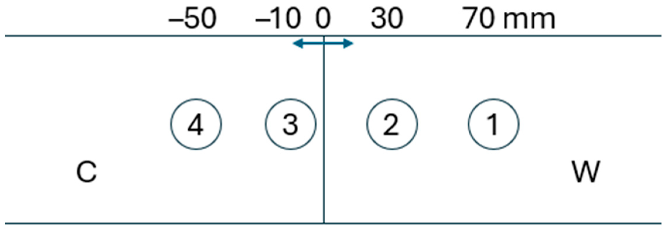
2. Materials and Methods

All coatings were deposited in an industrial PVD unit (Cemecon AG, Germany) utilizing just one sputter target sized 500 mm (length) × 88 mm (width). The target consisted of two segments of equal size, with tungsten at the top and graphite at the bottom (supplier: Avaluxe, Germany). Targets were screwed onto the cooled magnetron body using a 0.2 mm thick graphite foil to ensure sufficient heat transfer. Square turning inserts (SNGA, 12 × 12 mm) were used as samples made of either oxide ceramics or cemented carbide with 6 wt. % cobalt binder. Ceramic samples were used for analytics (EDS) to avoid tungsten underground signals. Carbide inserts were subject to erosive wear testing and XRD analysis. Sample flank faces were ground and polished to a mirror finish. Cleaning was carried out in an ultrasonically agitated detergent bath for 1 min at 50 °C, then rinsing with ethanol and wiping dry with a clean paper cloth (Kleenex type). Inserts were placed on a rod at a distance of 40 mm and positioned as shown in Figure 1 with respect to the segmented target. Pos. 1 is at 70 mm above the intersection (in front of the tungsten segment), and pos. 4 is located at −50 mm below (in front of the graphite segment). Initial studies showed that the most significant changes happen close to the intersection, with rapid hardness loss moving down the graphite target segment. All samples were rotated twofold (carousel and spindle driven by a gearbox).
The coating process itself consisted of the following steps: evacuation, radiation heating at about 700 °C (60 min), plasma etching (20 min), coating (60 min), and cooling to 250 °C before opening the coating chamber again. Mid-frequency argon etching was performed using bi-polar pulsing of the substrate table with a frequency of 240 kHz and a bias voltage of 650 V. Argon pressure was set to 0.25 Pa. Films were deposited in an argon atmosphere at 0.2 Pa base pressure. The temperature was reduced to approx. 500 °C during deposition. Table 1 summarizes the most important deposition parameters. A relatively high bias voltage was chosen to provoke noticeable differences. Bias was either kept constant at 175 V or in pulsed mode with a pulse length of 100 µs and delay of 50 µs relative to the onset of the target pulse (at a frequency of 2 kHz and on-time of 50 µs, i.e., a 10% duty cycle).
Coating thickness was determined by calotte grinding about 1 mm away from the sample edge and verified by XRF (Fischer XDAL). Thicknesses were in the range of 1.5–2 micron. The W:C elemental ratio was determined by EDS with a Phenom XL scanning electron microscope at 15 keV over an area of 130 × 130 µm (rounded average of two areas). Argon concentrations were obtained from XRF but just for qualitatively comparing any differences between the two bias pulse modes.
The mechanical properties of the films, such as universal hardness (HM), plastic hardness (Hpl), and reduced modulus (E), were measured by the nano-indentation method using a Fischerscope HM2000 according to ASTM E 2546. For better accuracy, the coated surface was polished at a slight angle to reduce the scatter of the loading/unloading curves. In order to keep the maximum indentation depth significantly smaller than the film thickness, a load of 10 mN was used without dwell time at maximum load, which resulted in a typical penetration depth of about 0.1 µm. Twelve indentations were performed on each sample, and the scatter of the results typically stayed below 5% (of the average value). Only plastic hardness is presented in this paper, as modulus was found to scale with hardness (H/E ~ 0.07).
The compressive stress σ of the films was determined by measuring the bending of steel strips (only coated on one side) according to the well-known Stoney equation:
σ = E × t2/[6(1 − v)d] × 1/R
where E, v, and t are properties of the steel strip (E = Young’s modulus, v = Poisson’s ratio, t = thickness), d is the thickness of the film deposited on the strip, and R is the radius of observed bending (coated surface of the strip bulging upward). X-ray analyses were performed with an MF600 unit (Rigaku, Japan) using Cu Kα radiation generated at a voltage of 40 kV and a 20 mA anode current. A Ni K beta filter was used in combination with a Soller slit size of 0.2 mm.
The resistance of the coated substrates against erosive wear was evaluated by dry blasting with alumina grit (average grain size of 40 µm). We chose this method to evaluate the performance of such coatings when exposed to a stream of hard particles (in a fluid or air-borne) when used, for instance, as a valve component. A pressure of 4 bar and a distance of approx. 100 mm were used. The duration of this treatment was 120 s. Material loss, i.e., wearing of the tested films, was determined by XRF measurement at 12 different locations on areas with and without treatment (serving as reference areas). The untreated surface was preserved by covering part of the flank surface with plastic tape so that no erosive attack could occur.

3. Results and Discussion

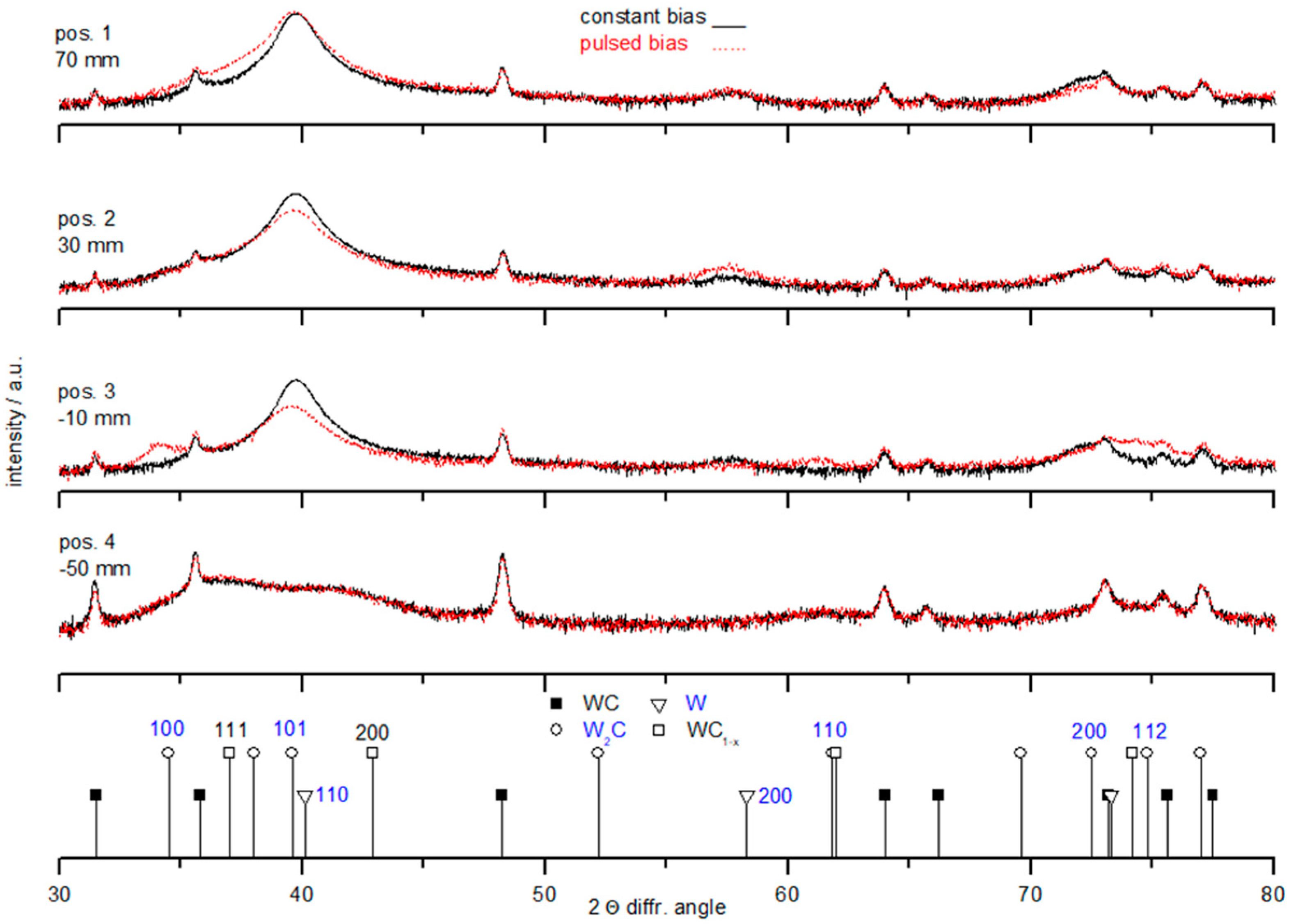
3.1. Coating Composition

Depending on the vertical positioning of the samples, concentrations of W and C will differ from top to bottom. Quantification of light elements, such as carbon, can be erroneous in EDS. So, initially, we measured a binderless reference sample of stoichiometric WC and obtained almost exactly the expected 50:50 (at. %). Therefore, we could go ahead with measuring all samples and take W:C readings of the instrument directly. The resulting values for both substrate bias voltage modes are listed in Table 2. As intended, the share of tungsten gradually decreases when moving from position 1 to 4 for both bias modes. Obviously, applying a pulsed bias voltage (with delay) leads to reduced tungsten and increased carbon contents when compared to the films deposited with constant bias. As sputtering was used in film deposition, argon can get embedded in the growing film. The argon concentration was obtained by XRF, and the value listed in brackets should be understood as just an indication (arbitrary units). Interestingly, Ar appears only in constant mode. Both trends can be explained by the findings of Hsu and Greczynski [13]. Applying a pulsed voltage with a delay to the substrates will minimize the argon bombardment, which arrives within less than about 40 µs after the pulse has started at the target itself. The less-mobile tungsten ions are delayed and arrive in larger numbers, starting at about 50 µm after the onset of the target pulse. With constant bias, there is a continuous bombardment with Ar+ that leads to the embedding of Ar in the growing film and significant re-sputtering of carbon. By using narrow bias voltage pulses, there will be much less bombardment of the growing film and consequently less re-sputtering and depletion of carbon. The decrease in Ar concentrations for films that are deposited with constant bias increasing the amounts of carbon may be explained by reduced crystallinity and stress of the film, as will be explained later.

3.2. Mechanical Properties

The plastic hardness and stress values of all films are visualized in Figure 2. The use of a pulsed bias leads to approx. 10% higher values, with a maximum hardness of 36 GPa just below the intersection of the segments. Compressive stresses increase from pos. 1 to 2 as the carbon content increases, with higher values for pulsed bias. It is interesting that the hardest films obtained at pos. 3 show the highest stress only for constant bias, whereas the value dropped considerably in the case of pulsed bias. Considering the W:C ratio (Table 2), it seems the stress is mainly driven by chemical composition and is comparable when comparing similar W:C ratios. The drop in hardness and stress at pos. 4 with the highest carbon content is likely due to the beginning of carbon precipitation [11].
For a better understanding, phase analyses by XRD, as shown in Figure 3, need to be discussed. Reflections of the substrate’s hexagonal WC phase are present but just as unchanging “background” signals and are not considered further. Films at positions 1–3 are dominated by a reflection from the W2C (101) plane. A minor presence of metallic tungsten can be inferred by the W (200) signal and possibly a concealed W (110) peak close to 40°. Position 3 is where most differences occur for the two bias modes. Whereas constant bias leads to virtually the same pattern as for position 2, pulsed bias reveals a weakening of W2C (101) and the occurrence of reflections of the (101), (102), and (110) planes. The weak W (200) signal is also gone in this case. Therefore, it is assumed that the higher compressive stress, especially for the film deposited with constant bias at position 3, is mainly due to lattice distortion of the tungsten phase by forced solution of carbon atoms. This is not the case for pulsed bias (the film at pos. 3), as the metallic phase is gone, and stress is relieved by the formation of different W2C crystal planes. Position 4 is again almost the same for both bias modes, with broad signals from the WC1-x (111) and (200) planes confirming the results of Abbad et al. [11]. This nano-crystalline structure leads to the lowest and identical stress values, possibly also due to the beginning of precipitation of unordered carbon. A TEM study would be needed to clarify the situation.

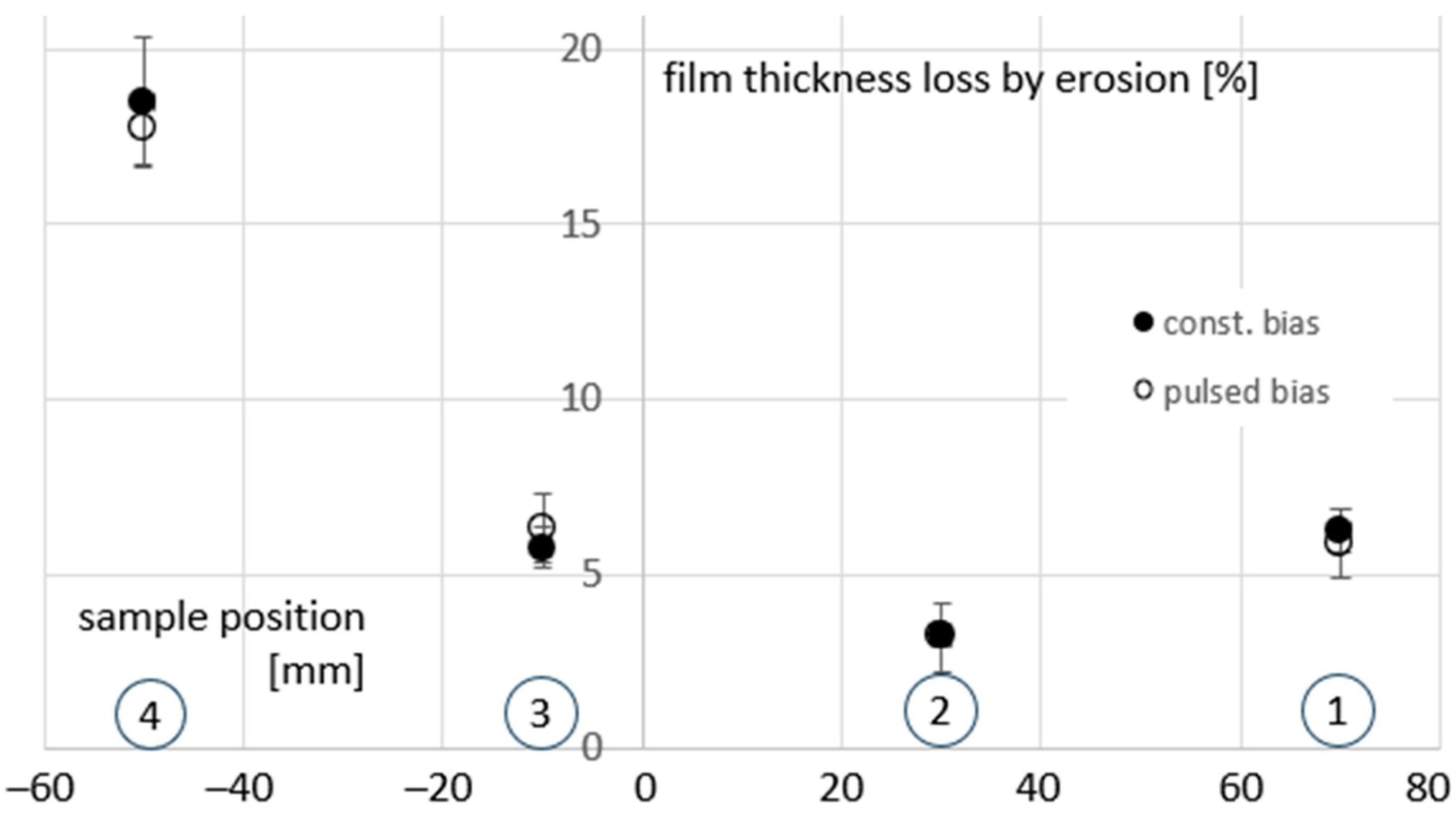
3.3. Erosive Wear Testing

The resistance of the W-C films against wear was tested by exposure to a stream of hard alumina particles, as specified in Section 2. Figure 4 shows the relative reduction of film thickness determined by XRF. The absolute reduction was not chosen to avoid distortion of thickness readings by changing W:C ratios. Instead, the relative decrease in percent relative to the initial coating thickness was taken. Results for all W-C coatings deposited in both substrate bias modes are shown. The curves reveal a very similar tendency. The softest coating (pos. 4) with a WC1-x phase also shows highest wear. However, the other coatings with H > 25 GPa hardness and all composed of mainly W2C wear comparably, losing 5–10% of their initial thickness regardless of the bias mode. It is also interesting that the hardest films of both bias modes do not offer the best protection. The reason for this saturation in wear resistance is possibly due to the highest brittleness.

4. Conclusions

Tungsten carbide films were deposited in an industrial-scale PVD unit capable of HiPIMS pulsing of both the cathode and substrate table. The W:C ratio was varied by sputtering a segmented target with a tungsten segment at the top and graphite (pure carbon) at the bottom. This allowed the sampling of multiple compositions in just one coating process, with a focus here on studying tungsten-rich compounds with the highest hardness. In addition, two modes of bias substrate voltage were applied, i.e., constant and pulsed bias (with a delay of 50 µs related to pulse onset at the sputter target). The W:C ratio decreased from about 90:10 at. % to roughly 60:40 at the vertical positions that were sampled. In pulsed bias voltage mode, no trapped Ar was detected, and carbon concentrations were systematically higher by 3–9 at. %, which was not reported before for HiPIMS of W-C. Both findings are explained by less intense bombardment compared to constant bias and capturing less Ar+ in each delayed bias pulse. The film’s crystal structure is dominated above 75 at. % W by hexagonal W2C with traces of metallic tungsten and cubic WC1-x below 60 at. % W. The highest hardness was achieved in the intermediate zone between the two segments when the W2C was about to convert to the WC1-x phase. Pulsed bias results in about 10% higher hardnesses for tungsten-rich coatings. However, we could not confirm reduced stress when applying a pulsed bias. In contrast to previous findings, tungsten-rich coatings that are W2C single-phased with about 80 at. % W showed the lowest material loss in erosive wear testing. As pointed out by other authors, if a sliding contact is involved (as in pin-on-disk testing), a low friction value becomes important, and carbon-rich films with reduced hardness are more wear-resistant than the hardest coatings dominated by the W2C phase. Further studies will include tribological testing and a direct comparison to co-sputtering with separated W and C targets (so that substrate rotation and the formation of graphitic nano-layers can have an effect).

Author Contributions

Conceptualization, J.K.; methodology, J.K.; validation, J.K. and C.B.; investigation, J.K. and C.B.; data curation, J.K.; writing—original draft preparation, J.K.; writing—review and editing, C.B.; visualization, J.K. All authors have read and agreed to the published version of the manuscript.

Funding

This research received no external funding.

Data Availability Statement

Data are contained within the article.

Conflicts of Interest

The research was conducted in the absence of any commercial or financial relationships that could be construed as a potential conflict of interest.

References

  1. Pauleau, Y.; Gouy-Pailler, P. Very hard solid-solution type tungsten carbon coatings deposited by reactive magnetron sputtering. Mater. Lett. 1992, 12, 157–160. [Google Scholar] [CrossRef]
  2. Voevodin, A.; O’Neill, J.P.; Zabinski, J.S. Tribological performance and tribochemistry of nanocrystalline WC/amorphous diamond-like carbon composites. Thin Solid Films 1999, 342, 194–200. [Google Scholar] [CrossRef]
  3. Quesnel, E.; Paulea, Y.; Monge-Cadet, P.; Brum, M. Tungsten and tungsten-carbon PVD multilayered structures as erosion-resistant coatings. Surf. Coat. Technol. 1993, 62, 474–479. [Google Scholar] [CrossRef]
  4. Rebholz, C.; Schneider, J.M.; Leyland, A.; Matthews, A. Wear behaviour of carbon-containing tungsten coatings prepared by reactive magnetron sputtering. Surf. Coat. Technol. 1999, 112, 85–90. [Google Scholar] [CrossRef]
  5. Ramirez Reyna, O.; Perez Alvarez, J.; Flores Martinez, M.; Rodriguez Castro, G.A. Evaluation of mechanical properties and tribological behavior of DLC/WC/WCN/W multilayer coatings deposited by HiPIMS. Mater. Lett. 2024, 357, 135737. [Google Scholar] [CrossRef]
  6. Efeoglu, I.; Totik, Y.; Gulten, G.; Yaylali, B.; Yesilyurt, M. Adhesion and friction-wear characterization of W-doped hydrogenated diamond-like carbon (a-C:H) coatings. Surf. Coat. Technol. 2025, 495, 131578. [Google Scholar] [CrossRef]
  7. Kurlov, A.S.; Gusev, A.I. Tungsten carbides and W-C phase diagram. Inorg. Mater. 2006, 2, 121–127. [Google Scholar] [CrossRef]
  8. Fuchs, K.; Rodhammer, P.; Bertel, E.; Netzer, F.P.; Gornik, E. Reactive and non-reactive high sputter deposition of tungsten carbide. Thin Solid Films 1987, 151, 383–395. [Google Scholar] [CrossRef]
  9. Wang, L.; Li, L.; Kuang, X. Effect of substrate bias on microstructure and mechanical properties of WC-DLC coatings deposited by HiPIMS. Surf. Coat. Technol. 2018, 352, 33–41. [Google Scholar] [CrossRef]
  10. Glechner, T.; Tomastik, C.; Badisch, E.; Polcik, P.; Riedl, H. Influence of WC/C target composition and bias potential on the structure-mechanical properties of non-reactively sputtered WC coatings. Surf. Coat. Technol. 2022, 432, 128036. [Google Scholar] [CrossRef]
  11. Abad, M.D.; Munoz Marquez, M.A.; El Mrabet, S.; Justo, A.; Sanchez Lopez, J.C. Tailored synthesis of nanostructured WC/a-C coatings by dual magnetron sputtering. Surf. Coat. Technol. 2010, 204, 3490–3500. [Google Scholar] [CrossRef]
  12. Song, R.; Chen, S.; Liu, Z.; Huo, Z.; Chen, Q. Effect of W-doping on the structure and properties of DLC films prepared by combining physical and chemical vapor deposition. Diam. Relat. Mater. 2023, 132, 109687. [Google Scholar] [CrossRef]
  13. Hsu, T.W.; Greczynski, G.; Boyd, R.; Kolozsvari, S.; Polcik, P.; Oden, M. Dense and hard TiWC protective coatings grown with tungsten ion irradiation using WC-HiPIMS/TiC-DCMS co-sputtering technique without external heating. Appl. Surf. Sci. 2023, 618, 156639. [Google Scholar] [CrossRef]
Figure 1. Schematic (rotated by 90°) of sample positioning in front of segmented target.
Coatings 15 00115 g001
Figure 2. Hardness and stress of W-C films at pos. 1–4 for both bias modes.
Coatings 15 00115 g002
Figure 3. X-ray diffraction diagrams for W-C films at pos. 1–4 for both bias modes (reference lines are taken from the ICDD database).
Coatings 15 00115 g003
Figure 4. Film thickness reduction by erosion wear testing of W-C films at pos. 1–4 for both bias modes.
Coatings 15 00115 g004
Table 1. Overview of deposition parameters (*: constant and pulsed modes).
Target PowerPulse Freq.Pulse On-TimePressureBias Voltage
6 kW2000 Hz50 µs0.43 Pa175 V *
Table 2. Elemental contents W:C (at. %) for the different positions (in mm) and bias voltage modes, with Ar concentrations in brackets (a.u.).
Bias Volt. ModePos. 1 (70)Pos. 2 (30)Pos. 3 (−10)Pos. 4 (−50)
constant90:10 (2)86:13 (1.5)79:21 (1)61:39 (0)
pulsed83:17 (0)78:22 (0)76:24 (0)55:45 (0)
Disclaimer/Publisher’s Note: The statements, opinions and data contained in all publications are solely those of the individual author(s) and contributor(s) and not of MDPI and/or the editor(s). MDPI and/or the editor(s) disclaim responsibility for any injury to people or property resulting from any ideas, methods, instructions or products referred to in the content.

