
Enhanced Wear and Corrosion Resistance of AZ91 Magnesium Alloy via Adherent Si-DLC Coating with Si-Interlayer: Impact of Biasing Voltage

Abstract
1. Introduction
2. Materials and Methods
3. Results
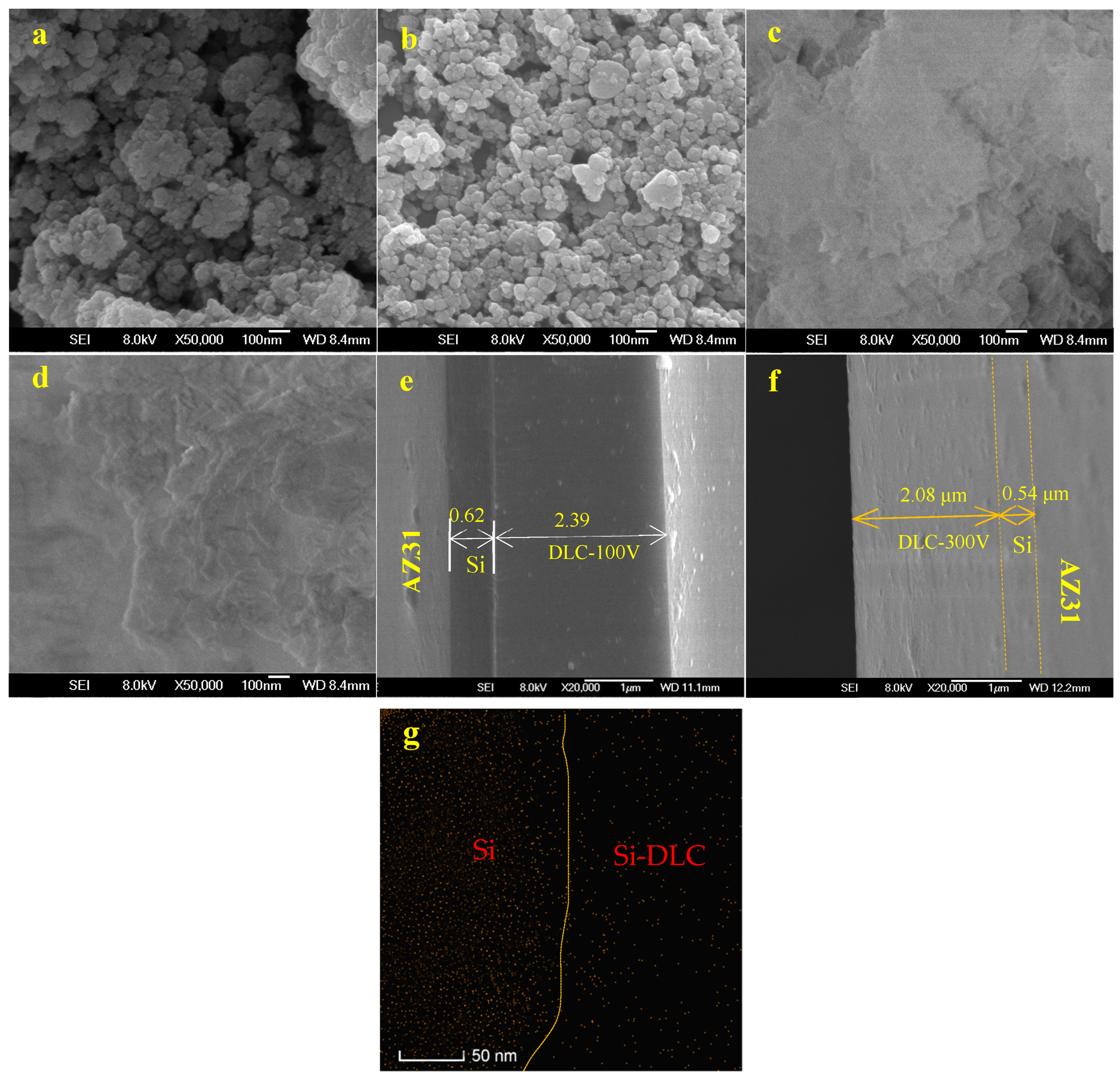
3.1. Structure
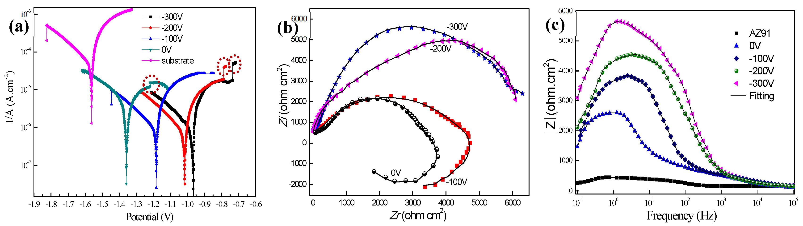
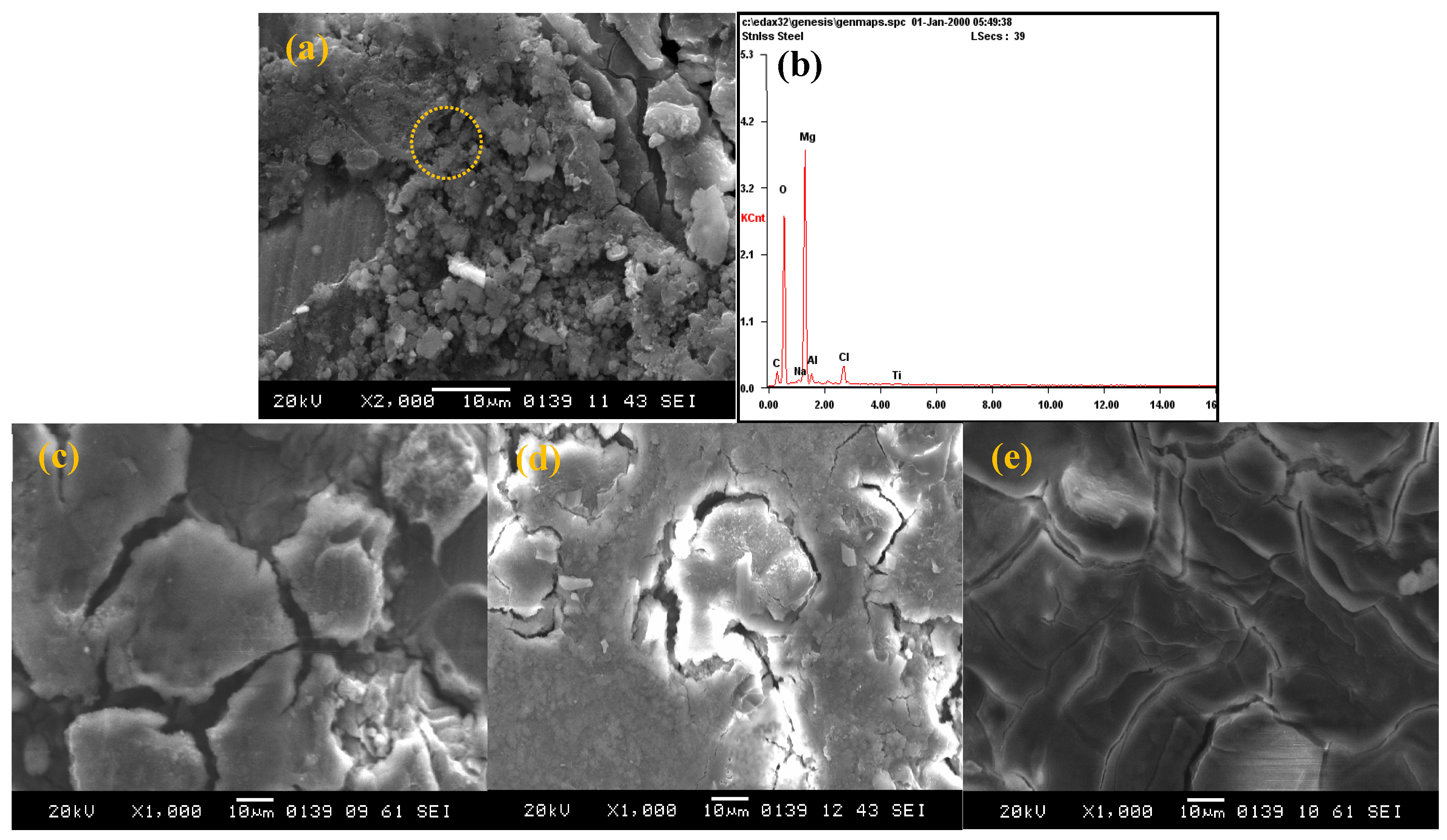
3.2. Corrosion Behavior
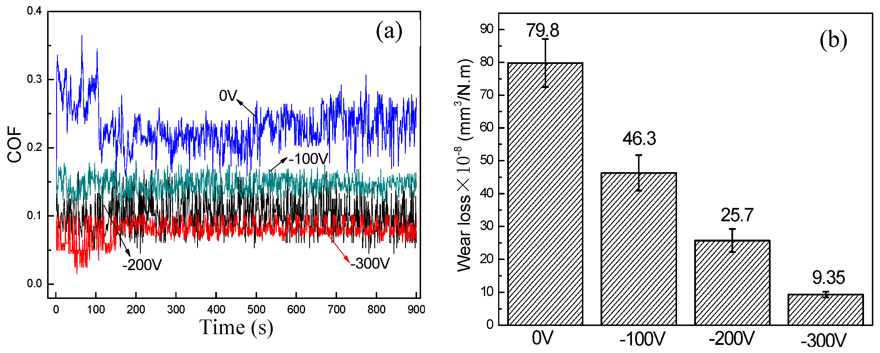
3.3. Tribological Property
4. Discussion
5. Conclusions
Author Contributions
Funding
Institutional Review Board Statement
Informed Consent Statement
Data Availability Statement
Conflicts of Interest
References
- Bai, J.Y.; Yang, Y.; Wen, C.; Chen, J.; Zhou, G.; Jiang, B.; Peng, X.D.; Pan, F.S. Applications of magnesium alloys for aerospace: A review. J. Magnes. Alloy. 2023, 11, 3609–3619. [Google Scholar] [CrossRef]
- Apelfeld, A.; Krit, B.; Ludin, V.; Morozova, N.; Vladimirov, B.; Wu, R.Z. The characterization of plasma electrolytic oxidation coatings on AZ41 magnesium alloy. Surf. Coat. Technol. 2017, 322, 127–133. [Google Scholar] [CrossRef]
- Ji, P.; Long, R.Y.; Hou, L.G.; Wu, R.Z.; Zhang, J.H.; Zhang, M.L. Study on hydrophobicity and wettability transition of Ni-Cu-SiC coating on Mg-Li alloy. Surf. Coat. Technol. 2018, 350, 428–435. [Google Scholar] [CrossRef]
- Li, H.T.; Wang, Q.; Zhuang, M.H.; Wu, J.J. Characterization and residual stress analysis of TiN/TiCN films on AZ31 magnesium alloy by PVD. Vacuum 2015, 112, 66–69. [Google Scholar] [CrossRef]
- Li, H.T.; Sun, P.F.; Cheng, D.H. Structure and properties of DLC films deposited on Mg alloy at different C2H2 flows of magnetron sputtering process. Coatings 2021, 11, 815. [Google Scholar] [CrossRef]
- Molak, R.M.; Topolski, K.; Spychalski, M.; Dulińska-Molak, I.; Morończyk, B.; Pakieła, Z.; Nieużyła, L.; Mazurkiewicz, M.; Wojucki, M.; Gebeshuber, A.; et al. Functional properties of the novel hybrid coatings combined of the oxide and DLC layer as a protective coating for AZ91E magnesium alloy. Surf. Coat. Technol. 2019, 380, 125040. [Google Scholar] [CrossRef]
- Dai, W.; Wu, G.S.; Wang, A.Y. Preparation, characterization and properties of Cr-incorporated DLC films on magnesium alloy. Diam. Relat. Mater. 2010, 19, 1307–1315. [Google Scholar] [CrossRef]
- Wu, Y.M.; Zhou, S.G.; Zhao, W.J.; Ouyang, L. Comparative corrosion resistance properties between (Cu,Ce)-DLC and Ti co-doped (Cu,Ce)/Ti-DLC films prepared via magnetron sputtering method. Chem. Phys. Lett. 2018, 705, 50–58. [Google Scholar] [CrossRef]
- Pillari, L.K.; Umasankar, V.; Sarma, A.; Gupta, M. DLC coating of magnesium nanocomposites using RF sputtering. Mater. Today Proc. 2017, 4, 6737–6742. [Google Scholar] [CrossRef]
- Zou, Y.S.; Wu, Y.F.; Yang, H.; Cang, K.; Song, G.H.; Li, Z.X.; Zhou, K. The microstructure, mechanical and friction properties of protective diamond like carbon films on magnesium alloy. Appl. Surf. Sci. 2011, 258, 1624–1629. [Google Scholar] [CrossRef]
- Su, Y.Y.; Gong, X.H.; Huang, W.J.; Zhang, T.F.; Hu, R.; Zhang, P.; Ruan, H.; Ma, Y. Enhancing the tribological property of Mo-doped DLC films in methanol using appropriate bias voltage. Diam. Relat. Mater. 2023, 135, 109795. [Google Scholar] [CrossRef]
- Li, H.T.; Sun, P.F.; Qi, A.T.; Zhang, S.J.; Zhang, F.T. Modulation of structure and corrosion behavior of Si-DLC coatings on AZ31 by applying a self-source bias. Ceram. Int. 2023, 49, 32193–32204. [Google Scholar] [CrossRef]
- Xia, L.F.; Sun, M.R.; Liao, J.X. The effect of negative bias pulse on the bonding configurations and properties of DLC films prepared by PBII with acetylene. Diam. Relat. Mater. 2005, 14, 42–47. [Google Scholar] [CrossRef]
- Bhowmick, S.; Sen, F.G.; Banerji, A.; Alpas, A.T. Friction and adhesion of fluorine containing hydrophobic hydrogenated diamond-like carbon (F-H-DLC) coating against magnesium alloy AZ91. Surf. Coat. Technol. 2015, 267, 21–31. [Google Scholar] [CrossRef]
- Cui, C.Q.; Yang, C.Y. Study of Structural, Mechanical, and Corrosion Resistance of a Nanocomposite CrSiN/CrN/Cr Coating Deposited on AZ31: Effects of Deposition Time. Coatings 2023, 13, 678. [Google Scholar] [CrossRef]
- Li, H.T.; Sun, P.F.; Cheng, D.H.; Liu, Z.M. Effects of deposition temperature on structure, residual stress and corrosion behavior of Cr/TiN/Ti/TiN films. Ceram. Int. 2021, 47, 34909–34917. [Google Scholar] [CrossRef]
- Xu, F.M.; Luo, L.; Xiong, L.; Liu, Y. Microstructure and corrosion behavior of ALD Al2O3 film on AZ31 magnesium alloy with different surface roughness. J. Magnes. Alloys. 2020, 8, 480–492. [Google Scholar] [CrossRef]
- Cao, H.S.; Qi, F.G.; Ouyang, X.P.; Zhao, N.; Zhou, Y.; Li, B.; Luo, W.; Liao, B.; Luo, J. Effect of Ti Transition Layer Thickness on the Structure, Mechanical and Adhesion Properties of Ti-DLC Coatings on Aluminum Alloys. Materials 2018, 11, 1742. [Google Scholar] [CrossRef] [PubMed]
- Jedrzejczak, A.; Szymanski, W.; Kolodziejczyk, L.; Sobczyk-Guzenda, A.; Kaczorowski, W.; Grabarczyk, J.; Niedzielski, P.; Kolodziejczyk, A.; Batory, D. Tribological Characteristics of a-C:H:Si and a-C:H:SiOx Coatings Tested in Simulated Body Fluid and Protein Environmentnt. Materials 2022, 15, 2082. [Google Scholar] [CrossRef] [PubMed]


| Samples | Position (D Peak) (cm−1) | Position (G Peak) (cm−1) | ID/IG | FWHM of G Peak (cm−1) | H at.% |
|---|---|---|---|---|---|
| 0 V | 1351.7 | 1580.1 | 1.26 | 74.69 | 18.35 |
| −100 V | 1358.5 | 1582.3 | 1.09 | 70.18 | 14.07 |
| −200 V | 1365.2 | 1584.6 | 0.72 | 67.92 | 10.84 |
| −300 V | 1367.5 | 1587.1 | 0.47 | 65.67 | 6.29 |
| Samples | Ecorr (V) | Icorr (A·cm−2) | Rcorr (mm/Year) | βc (mV) | βa (mV) |
|---|---|---|---|---|---|
| AZ91 | −1.566 | 7.84 × 10⁻⁴ | 17.77 | 480 | 322 |
| 0 V | −1.359 | 9.98 × 10⁻⁶ | 0.258 | 467 | 84 |
| −100 V | −1.185 | 7.45 × 10⁻⁶ | 0.193 | 311 | 88 |
| −200 V | −1.016 | 5.89 × 10⁻⁶ | 0.152 | 309 | 49 |
| −300 V | −0.967 | 6.02 × 10⁻⁶ | 0.156 | 226 | 40 |
Disclaimer/Publisher’s Note: The statements, opinions and data contained in all publications are solely those of the individual author(s) and contributor(s) and not of MDPI and/or the editor(s). MDPI and/or the editor(s) disclaim responsibility for any injury to people or property resulting from any ideas, methods, instructions or products referred to in the content. |
© 2024 by the authors. Licensee MDPI, Basel, Switzerland. This article is an open access article distributed under the terms and conditions of the Creative Commons Attribution (CC BY) license (https://creativecommons.org/licenses/by/4.0/).
Share and Cite
Cui, C.; Yang, C. Enhanced Wear and Corrosion Resistance of AZ91 Magnesium Alloy via Adherent Si-DLC Coating with Si-Interlayer: Impact of Biasing Voltage. Coatings 2024, 14, 341. https://doi.org/10.3390/coatings14030341
Cui C, Yang C. Enhanced Wear and Corrosion Resistance of AZ91 Magnesium Alloy via Adherent Si-DLC Coating with Si-Interlayer: Impact of Biasing Voltage. Coatings. 2024; 14(3):341. https://doi.org/10.3390/coatings14030341
Chicago/Turabian StyleCui, Changqing, and Chunyan Yang. 2024. "Enhanced Wear and Corrosion Resistance of AZ91 Magnesium Alloy via Adherent Si-DLC Coating with Si-Interlayer: Impact of Biasing Voltage" Coatings 14, no. 3: 341. https://doi.org/10.3390/coatings14030341
APA StyleCui, C., & Yang, C. (2024). Enhanced Wear and Corrosion Resistance of AZ91 Magnesium Alloy via Adherent Si-DLC Coating with Si-Interlayer: Impact of Biasing Voltage. Coatings, 14(3), 341. https://doi.org/10.3390/coatings14030341