1. Introduction
Interest in copper thin films as a subject of material science has been growing due to their outstanding properties, including their high electrical conductivity, flexibility, and ductility [
1,
2,
3,
4]. However, copper films have some disadvantages, such as their tendency to oxidize in air, which negatively influences their conductivity and even alters their color. Therefore, protective coatings are needed for certain applications [
5,
6]. These films retain the intrinsic ductility of bulk copper and exhibit exceptionally high malleability, allowing them to be bent or folded easily without fracturing [
7,
8]. This flexibility facilitates the development of wearable and flexible electronics, enabling new frontiers in technology using fabrics and other substrates [
9]. Such advancement holds particular significance in the fast-growing areas of wearable technologies and smart textiles.
The exceptional electrical conductivity, flexibility, and substrate adherence characteristics of copper thin films make them indispensable in modern electronics [
4,
10,
11]. They are widely used in integrated circuit interconnects due to their speed and reliability in transmitting signals. With the miniaturization of devices, copper thin films play a very pivotal role in enabling efficient circuit fabrication [
12]. Additionally, their ductility makes these materials suitable for flexible electronics, including bendable gadgets, wearables, and smart textiles. High thermal conductivity allows for enhanced heat dissipation, thereby protecting the electronic components from overheating, which could otherwise result in a damaged gadget or poor performance in high-power applications [
13].
Copper thin film deposition plays a prominent role in the miniaturization and development of nanoscale electronic performance [
14]. The general deposition techniques include sputtering, atomic layer deposition, chemical vapor deposition, and electroplating [
14]. Although sputtering and electroplating techniques offer industrial scalability, atomic layer deposition (ALD) and chemical vapor deposition (CVD) ensure high-purity film deposition with precision, making them suitable for microelectronic applications. Optimizations regarding grain structure, morphology, and the conductivity of copper films have been made to extend their applications in sensors and flexible electronics [
15]. However, issues such as oxidation and diffusion remain central to research that aims to fine-tune deposition parameters and explore novel solutions for specific applications [
16,
17].
Extensive studies have been conducted regarding the electrical and mechanical responses of metallic films deposited on flexible substrates, whereas only minimal studies have examined copper thin films subjected to only tensile stresses [
18,
19]. Their mechanical deformation and electrical properties must be investigated to understand their behavior in strained states and the implications for material mechanics and nanoscale metal behavior [
20]. Mechanical stress and reliability make copper films suitable for flexible devices, such as wearable electronics and medical technologies, which require survivability under mechanical strain.
Grain orientation, temperature, and strain energy are the factors that influence the mechanical behavior of copper films. Investigations have found that copper films exhibit rapid stress relaxation at high temperatures due to surface diffusion, unlike aluminum films, for which enhanced strength arises from stable oxide layers [
21,
22]. According to mechanical analyses using biaxial bulging and uniaxial tensile tests, copper thin films usually possess higher strength but lower ductility compared to bulk copper. This highlights the need for strategies that can optimize their properties [
23].
Recent developments in metallic materials for multifunctional applications corroborate the above observations. For example, in situ-generated nanoparticles of TiC in a copper matrix significantly enhance hardness and ductility, consistent with the increased reliability of films under tensile stress [
24]. Severe plastic deformation techniques may indicate that metallic materials can be strengthened via nanostructural design. Different strengthening mechanisms have been discussed for metallic materials in relation to crack initiation and propagation [
25]. Research on nanowires and ultrathin films has focused on optimizing nanostructures for high conductivity and flexibility; thus, this work is highly relevant to the study of copper thin films for flexible electronics [
26,
27].
Stress-driven phenomena, such as cracking and buckling, are common features in thin films that affect functionality and performance. Despite the research on molybdenum, chromium, and aluminum films, copper thin films present peculiar phenomena, such as gradual cracking under tensile stress, and the direct impact on electrical resistance is documented in [
28,
29,
30,
31]. In this paper, crack morphology and electrical degradation are further investigated in copper films, focusing in particular on film thickness and strain sensitivity. In comparison, this is where copper’s disparate electrical and mechanical responses to tensile loading stands out, especially when compared to other materials, such as indium tin oxide and Poly(3,4-ethylenedioxythiophene) (PEDOT) films [
32].
The work presented here introduces new insights related to crack initiation and crack propagation with respect to PCER under controlled tensile loading. While many research efforts have focused on copper thin films in terms of deposition techniques and general properties, few studies have exclusively dealt with the correlation between film thickness, mechanical strain, and electrical resistance. The obtained results are crucial for optimizing copper thin films for applications in flexible electronics and wearables, offering useful information for future technological development.
This work examines the nucleation and propagation of cracks in copper thin films due to tensile stress using scanning electron microscopy. Electrical resistance, as measured by a two-point probe ohmmeter, is correlated with strain to understand how mechanical deformation affects conductivity degradation across films of varying thickness. These findings provide detailed information about the dependencies of strain sensitivity as opposed to mechanical durability, which are mandatory to advance the structural and functional reliability of copper thin films. The insights gained will contribute to the development of flexible device technologies and establish a basis for future studies in this rapidly evolving field.
2. Research Methodology
At the beginning of the experiment, 127 µm thick PET substrates were cut into identical pieces using razor-sharp knives. The pieces were cut identically to 10 mm × 100 mm. After being cut, the substrates were cleaned and dried with extreme care to eliminate the surface impurities to ensure the best sputtering conditions. Preliminary cleaning may be performed by removing obvious contaminants, dust, or grease from the substrate using lint-free wipes, soft brushes, or compressed air. Degreasing is carried out by soaking the substrate in acetone or isopropyl alcohol to dissolve oils, followed by rigorous washing with clean acetone or isopropyl alcohol or deionized water to remove any residue. The substrates were then positioned in the sputtering chamber with a copper target. A high-quality copper target was used during the sputtering process, ensuring consistent deposition parameters. This approach resulted in fine, uniform thin films with excellent thickness control, as evidenced by the SEM images and the uniformity of the as-deposited films presented in the manuscript. These high-quality films provided a reliable baseline for subsequent mechanical and electrical testing. To provide a vacuum, the chamber was sealed, and an atmosphere was internally evacuated down to a pressure of 2.5 × 10⁻³ Pa or lower. In this case, radio frequency magnetron sputtering with an RF power of 250 W and argon gas flow of 29 sccm was used. The substrates were rotated at 20 rpm during deposition to homogeneously coat the substrates. Under such conditions, controlled one-hour deposition yielded a copper layer of 100 nm in thickness. Conversely, upon increasing the time for sputtering to two hours, a copper film of 200 nm was produced; both thicknesses were thus prepared. Precision cutting associated with substrate preparations, along with the sputtering settings, resulted in specimens with a uniform copper coating. The thickness was determined using a quartz crystal microbalance (QCM) from Beijing Technol Science Co., Ltd., Beijing, China, a widely used companion device for most sputtering systems to measure film thickness in situ. QCM operates by detecting changes in the frequency of a vibrating quartz crystal, where the frequency shift is directly correlated with the thickness of the deposited film. The thickness was selected based on the requirements for flexible electronics applications. In such applications, the thickness typically ranges from 50 nm to 500 nm. The selected thicknesses of 100 nm and 200 nm are well within this range and are considered highly appropriate. These points have been added to the text for clarification.
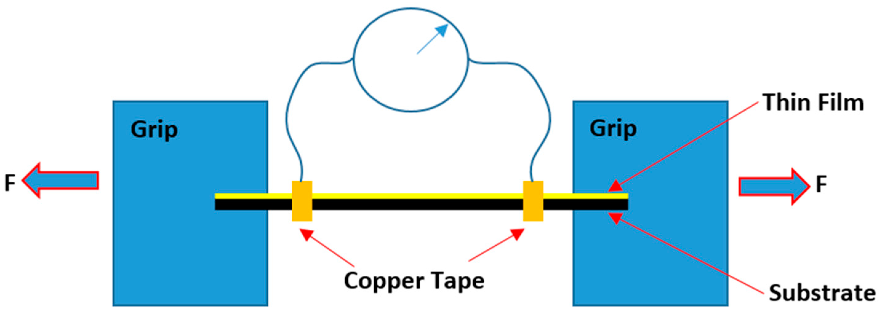
The sputtered samples were clamped on both ends with Instron grips placed 80 mm apart. In electrical resistance measurements, the ohmmeter terminals attached to the sides of the thin film with the help of copper tape were positioned 10 mm away from the grip ends, thus creating 60 mm of distance between the two terminal ends on the sample.
Figure 1: the upper grip was moved upwards at a steady rate of 1 mm/s until the final fracture of the specimen. Electrical resistance was measured and recorded continuously by using appropriate software.
A key objective of the experiment was the examination of the changes in electrical resistance during the stretching process, related to the percentage change in electrical resistance (i.e., ∆R/R0 × 100%). The work also researched the relationship between the percentage change in PCER and the magnitude of strain. To quantify the changes that occurred in the thin films upon stretching, SEM pictures were taken for samples that were stretched to strains of 2.5%, 7.5%, 10%, and 13.75%. This became a more precise means to determine what changes were occurring inside the thin films as they were being subjected to different amounts of strain. The levels were selected to capture a wide variation in deformation behavior, from the development of initial cracks to a stage where the crack has been fully developed. The lower strain levels, such as 2.5%, were included to capture the onset of mechanical and electrical changes associated with crack initiation. The intermediate levels were 7.5% and 10%, which were chosen to investigate crack development; the highest level of strain was 13.75%, corresponding to the final stages of crack development and its influence on electrical resistivity.
This range of values was selected to allow the adequate investigation of mechanical and electrical responses in the copper thin films under different levels of tensile stress. We hope that this explanation has clarified why these percentages have been chosen.
3. Results and Discussion
The present work presents novel insights regarding mechanical and electrical behaviors under tensile stress of copper thin films, where special emphasis is placed on the film thickness effect. While much work has been conducted regarding general copper films and their deposition methods, our work reveals for the first time the specific relationship between crack morphological evolution and the resultant electrical resistance change as a function of PCER. New insights into the interplay of mechanical deformation and electrical performance upon mechanical stretch illuminate new avenues for further advances in flexible electronics. The results also show that thicker films have a higher delay in crack initiation but are more sensitive to PCER at an advanced level of strain, which has not been extensively discussed in the literature. This work is bridging the gulf between mechanical reliability and electrical performance, being among the greatest challenges facing the design of flexible electronic devices. This welcome addition to the field of research not only involves conducting experiments and acquiring results but also contextualizing them within the recent progress on the microstructure and electrical properties of thin films. It further emphasizes the potential enabling applications for next-generation wearable sensors and flexible circuits.
The microstructure and composition of the deposited copper films were investigated by XRD (Alvord Systems Inc., Clairton, PA, USA) and EDS (JEOL Ltd., Tokyo, Japan)., respectively.
Figure 2: Left: the XRD patterns of 100 nm and 200 nm copper films showing a polycrystalline nature, with the predominance of peaks for Cu(111) and Cu(200). The results obtained thus far, therefore, indicate that high-quality copper films with well-defined crystalline orientations have been successfully deposited. Additionally, EDS was performed on the elemental composition of the 200 nm film, as illustrated in
Figure 1 (right). In this spectrum, the characteristic peaks for Cu Lα, Cu Kα, and Cu Kβ are notable, confirming copper as the major constituent element. Indeed, this underscores the purity and homogeneity of the deposited film. The above analyses confirm that the copper thin films are structurally and compositionally intact, thereby supporting their suitability for mechanical and electrical testing in the current work.
Figure 3 and
Figure 4 depict the SEM (JEOL Ltd., Tokyo, Japan) images of the as-deposited copper thin films with thicknesses of 100 nm and 200 nm, respectively. Both films reveal a smooth surface morphology without any visible cracks, indicating high-quality deposition. In such images, uniformity is realized, thus defining consistent baseline properties for further mechanical and electrical characterization under tensile stress. The crack initiation and propagation were monitored as a function of the increase in strain for both thicknesses.
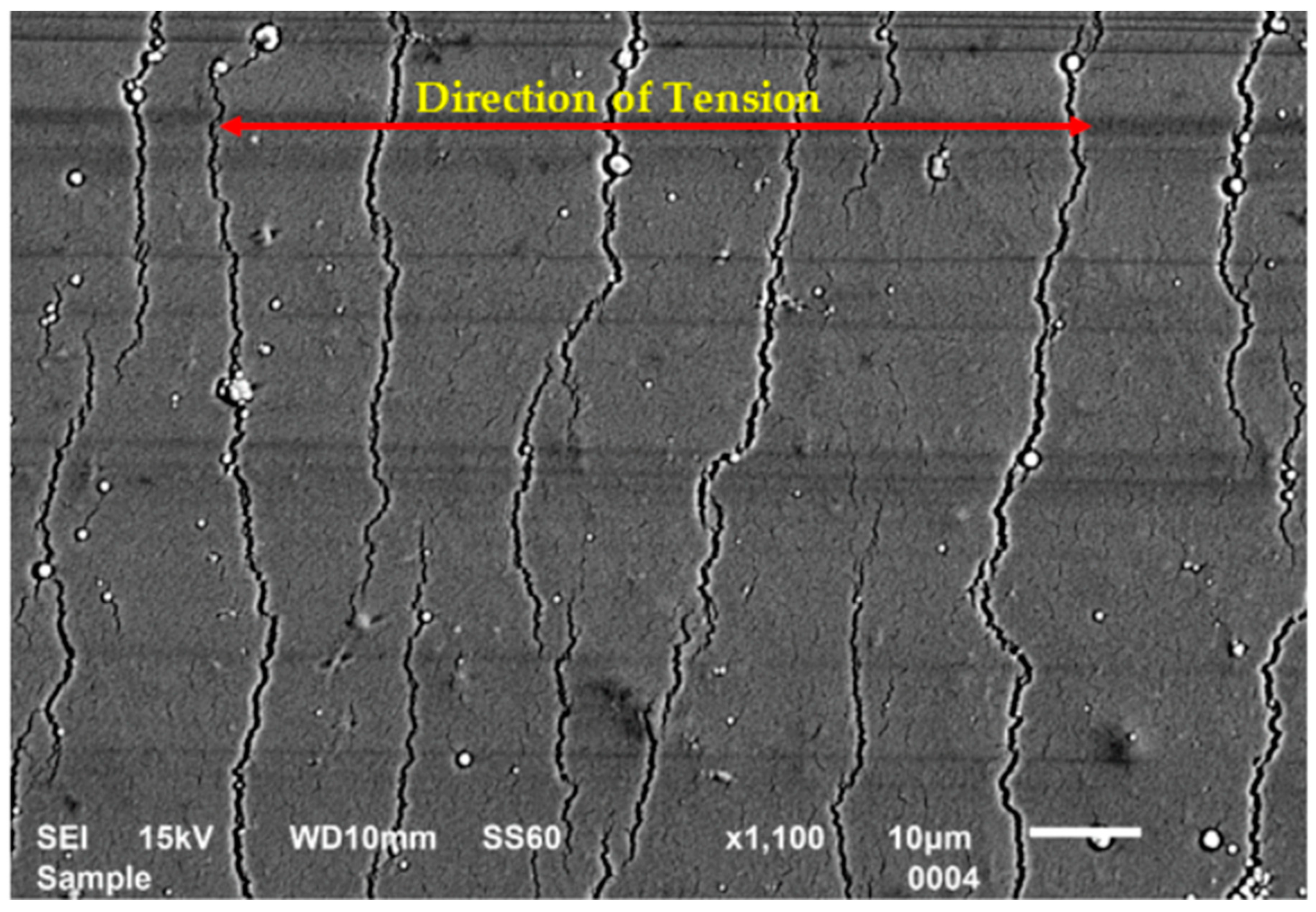
Figure 5 represents an SEM image of a copper thin film with a thickness of 100 nm, which was subjected to progressive stretching; the development of crack patterns under strain is shown. At the beginning of strains of 2.5%, the film exhibits initial cracks in the form of channels across the width of the sample perpendicular to the direction of the applied load. Deviations from linearity in such idealized linear cracks take a path other than perfectly straight, while crack faces mostly denote small angular deviations (less than 30 degrees) where it veers briefly to one side (e.g., to the right) and then returns to its forward path in either a zigzag or meandering course. The possible causes for this linearity might be due to several factors inherent to the material and to the loading conditions. The probable causes of such deviations in crack growth may be due to microstructural heterogeneities that, with grain boundaries, defects, or minor variations in thickness, perhaps could engender local stress concentrations and, therefore, slight deflections in the path of crack growth. Indeed, the presence of such imperfections upsets the homogenous course of the cracks, which adjusts their direction as they encounter regions of varying mechanical properties.
Such a behavior is presumably related to the ductile nature of the copper film. Indeed, in the case of ductile materials, crack propagation proceeds by way of a local plastic deformation process in which the material flow precedes the growth of cracks. Due to inhomogeneous distributions in the stress around a crack tip during stretching, material yield may occur locally and make the crack slightly deflect from its expected course before realigning with the tensile direction.
At 7.5% strain, the cracks have further widened and lengthened, with some of the cracks having started to branch and interlink; this is already indicative of a local failure in the film. In
Figure 6, in addition to the main cracks developed at 2.5% strain, a finer mesh-like crack network appears between these initial cracks. The inset in
Figure 6 illustrates the creation of fine mesh-like cracks. This second-order network suggests further material degradation, which is most likely driven by stress redistribution and localized strain intensification. These newer, finer cracks interweave between the existing ones, demonstrating the complexity of crack development under increasing strain, as shown in
Figure 7. The uniformity observed at lower strains gives more localized stress variations that start to disrupt the more homogeneous pattern of deformation.
At 10% strain, crack patterns are even more complicated, with excessive branching and further interconnection, revealing the material response to be even more pronounced. The original cracks continue propagating with the finer, mesh-like cracks formed at 7.5% strain, and the overall cracking is no longer uniform, implying significant variance in the film’s microstructural integrity or non-uniformity in the applied stress (
Figure 7). That level of strain clearly indicates a transition from the crack behavior described above, and the non-linear nature of the deformation of the material was further focused on inhomogeneity under additional tensile straining. The strain in copper film at 13.75% is characterized by a dense network of wide chaotic cracks, indicating intensive material damage. The linear cracking pattern of the film has completely disappeared, and the chaotic fracture network testifies that this material approaches its failure point (
Figure 7). The heavily cracked areas are bound to be the points that have experienced extreme loss in material integrity and might lead to complete failure upon further straining. As further straining increases, these initial cracks start growing both in width and length and continue spreading under the tensile load. Cracks begin to branch and interact with one another, forming a complex network of interlinking fractures. This interaction causes the redistribution of stresses within the film and thus forms new cracks at uncracked locations. These new cracks are small and localized around the so-called stress concentrators. Both crack branching and merging are manifestations of the progressive material damage involved in the elastic–plastic transition that the film undergoes. At higher strain levels, the coalescing of the cracks becomes more prominent with larger, interlinking fractures. At this stage, a critical transition of the failure mechanism occurs, since the residual load-carrying capability of the film decreases significantly. Non-linear crack propagation accelerates, and the material loses its global structural integrity. A transition from ductile behavior, where limited plastic deformation occurs with controlled crack growth, to a more brittle regime characterized by much faster growth signals that the film is approaching its mechanical limits. This understanding of the ductile-to-brittle transition will have important implications for the performance predictions of the mechanical loading of thin films and their reliability in diverse applications.
Figure 8,
Figure 9,
Figure 10,
Figure 11 and
Figure 12 through 12 depict a 200 nm copper thin film that has been stretched to 2.5%, 7.5%, 10%, and 13.75% of its original length, respectively. While the general pattern of crack development and morphology is quite similar to that observed in 100 nm thin films, subtle differences emerge upon close examination. These are discussed in greater detail in a comparative discussion regarding the two thicknesses. Various elements can be derived from crack formation and propagation when comparing copper thin films at 200 nm and 100 nm under mechanical strain. Due to the smaller area that the stress can be distributed through, the 100 nm copper thin film may develop cracks at lower strain levels. Cracks initiate faster because the thinner film is incapable of dissipating the stress being placed upon it. Conversely, the 200 nm film most likely has a higher threshold of strain for crack development due to its increased thickness. This additional volume of material would enable it to absorb stress and redistribute it better, causing the delay in crack formation. In other words, 200 nm film can sustain more deformation before cracking. The observation reflects higher ductility. Following crack nucleation, the crack propagation rate in the 200 nm film is slow compared to the 100 nm film. The greater thickness of extra material supplies greater resistance to crack advancement, with more energy dissipating before significant crack growth. Additionally, the morphology of the cracks in the 200 nm film may be different from that in the 100 nm film. In the thicker film, larger plastic deformation at the crack tips results in a wider, rougher crack. This plastic deformation is characteristic of ductile fracture, in contrast to the potentially sharper, more brittle fracture surfaces observed in the thinner film.
The crack density, or the number of cracks per unit area, is also likely to be lower in the 200 nm film at comparable strain levels. The larger deformation capability without the crack generation of the thicker film, as is common for ductile materials, reduces the number of occurring cracks. Moreover, some ductile tearing can take place in the 200 nm film, characterized by more rugged fracture surfaces, compared to the 100 nm film, where the limited volume of the material is expected to produce a more brittle fracture pattern. A further point of differentiation can be made based on the interaction of the crack path with the film’s microstructure. For the 200 nm film, one could expect to see intergranular cracking at grain sizes larger than its thickness, wherein the cracks would propagate along grain boundaries. In relation, the smaller grain size relative to thickness in the 100 nm film can enhance transgranular cracking because the cracks directly pass through the grains, since there is not much space to deflect. Surface topography also plays an important role in the crack formation process, as well as pre-existing defects. In the case of a 200 nm film, plastic deformation or a pile-up of material at the grain boundaries may be more clearly visible before crack formation, which would indicate stronger behavior against the strain for this film. Pre-existent defects, inclusions, or impurities will affect crack nucleation and propagation differently in a thicker film due to its greater volume of material, thus providing more opportunities for the better redistribution of stresses and further delays of the failure process.
While the study of copper thin films has uncovered distinct differences in the initiation, propagation, and morphology of cracks, contrasting the findings with those referenced, experiments on molybdenum-coated PET films by [
29] have demonstrated that the majority of crack initiation events occur perpendicular to the applied strain, with more irregular patterns for greater thickness and at higher strain rates. In the related work of [
30], for example, cracks in molybdenum thin films were observed to grow with secondary branching at specific angles, indicating material stress anisotropy. By contrast, the nucleation of cracks in our copper films was highly uniform for low strain levels, and the crack growth path was more linear, with fewer secondary branches, potentially indicating higher material ductility for copper.
The authors of [
31] reported that the Al thin films started to develop cracks at 2% strain, and with further strains, the crack morphology became complicated and resulted in lateral cracks. This phenomenon is somewhat consistent with our work, but copper films manifested crack formations at slightly larger strain levels due to their capacity for larger elongation prior to fracture. Meanwhile, two types of cracks were present in ITO thin films, as identified by [
32], namely, the cracks propagating perpendicular to the load and the secondary cracks branching off the primary ones at higher strains. We obtained a less pronounced degree of branching, further underlining the material-dependent nature of crack evolution. Furthermore, crack development has been reported by many other authors [
33,
34,
35].
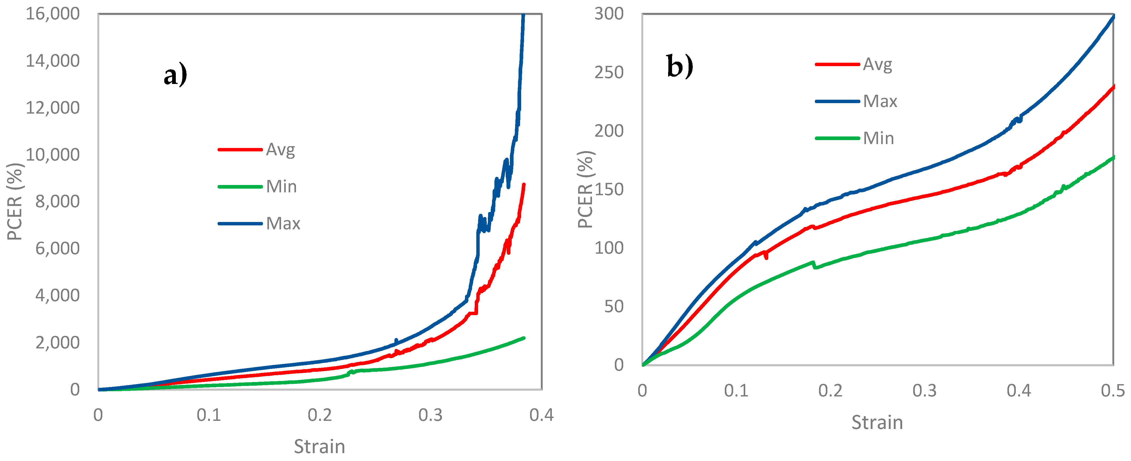
Figure 13 illustrates the mechanical strain–PCER relationship in copper thin films of different thicknesses. The mechanical strain–PCER plots present the average, minimum, and maximum PCER values obtained by four samples, in each case with the purpose of providing information about how the electrical resistance develops when the mechanical strain increases.
In
Figure 13a, the plots illustrate that the copper films have a thickness of 100 nm, and a trend can be identified wherein the PCER increases gradually as a function of strain. Beyond a certain strain threshold, the PCER does indeed increase steeply (at least its maximum values increase), suggesting that at higher strains, the electrical resistance of the film becomes substantially more sensitive to deformation. The mean curve passes through a smooth but non-linear transition as the strain increases, thereby attesting to some scatter in the response of individual specimens to strain. This may be due to the thinner cross-section of the film, which is more susceptible to localized deformation and changes in the microstructure, which in turn affect electrical properties.
In contrast,
Figure 13b, corresponding to copper films 200 nm thick, illustrates a more homogeneous and progressive rise in the PCER with strain. At high strains, the increase in PCER is also not as steep as in the case of 100 nm films. It further presents lower maximum PCER values compared to the 100 nm films, proving that the thicker films are insensitive to strain. The average response curve is similar in all the samples, featuring a gradual, smooth rise in the PCER, while this reflects the capacity of the thicker film to distribute the applied stress more evenly and resist a localized deformation.
By comparing these two figures, one may note that copper films are less sensitive to mechanical strain upon increases in film thickness. This lesser sensitivity was expected, as thicker films can distribute applied mechanical stress over a larger volume, thereby diluting effects at the same quantity of electrical resistance due to strain, whereas the thinner films, having a lower volume of material to distribute the stress in them, have larger changes in resistance and thus exhibit higher sensitivity to mechanical deformation.
These observations have practical implications as well. For example, for applications such as sensors, for which high strain sensitivity is required, a copper film with a higher PCER response would be preferable and therefore would be thinner in nature. Conversely, in applications where a wide range of strain requires more gradual or controlled changes in resistance, the thicker film may become more relevant. Of course, insights drawn from such PCER data should be considered in relation to other factors, such as mechanical stability, overall integration on devices, and the operational environment, which could all affect the long-term performance and reliability of the film.
It has been confirmed that PCER during tensile stress is the most important characteristic of film performance, representing the whole process of crack propagation in sub-micrometer metal films. The gradual increase in PCER, accompanied by sharp rises, corresponds to the last stages of the crack-formation process in the copper thin films studied here. Reference [
29] observed a very similar trend in molybdenum films, where PCER continued to increase with strain in a steady fashion, up until it exhibited a sudden surge at a higher magnitude of strain in the thicker films. Their results also indicated certain partial recoveries at the tail of PCER curves—presumably due to possible conductive realignments that were not realized in these copper films.
On the other hand, [
31] measured a substantially faster increase in PCER in aluminum thin films with crack propagation, with a strong dependence on film thickness. This attests to the more brittle nature of aluminum relative to copper. Indeed, [
32] showed that ITO films had a higher PCER sensitivity to strain when compared with PEDOT films; this was consistent with our results regarding copper’s behavior between brittle and ductile materials. Furthermore, [
30] indicated that thickness and strain rate are the two most influential parameters of PCER in molybdenum-coated films, whereas in the present study, thickness was determined to be a main factor for copper films, and the importance of the strain rate was low.
4. Conclusions and Recommendations
The present work provides an overview of the mechanical and electrical behaviors of copper thin films of two different thicknesses, namely 100 nm and 200 nm, under tensile stress. The results underline the importance of film thickness in relation to the response of the film to strain. While the thinnest films tested (100 nm) indicated higher sensitivity to mechanical deformation, with a more pronounced increase in PCER due to crack initiation and propagation at an early stage, 200 nm films exhibited greater ductility, with crack formation considerably delayed and an increase in PCER more gradual. This thickness-dependent behavior underlines the trade-off between strain sensitivity and mechanical durability in Cu films and underscores their applicability for flexible electronics and strain-sensitive sensors.
The results also suggest that with increasing strain, crack morphology evolves progressively from linear, well-defined cracks at low strains to complex branched crack networks at higher strains. The observed evolution of crack patterns with large increases in electrical resistance is especially pronounced for thinner films and suggests that the microstructural integrity of the film is severely degraded under high tensile stress. The results obtained herein provide further insight into the mechanical behavior of copper thin films, especially with respect to their electrical properties, and open an avenue toward the optimal design of copper-based thin films for specific applications.
Applications that require high strain sensitivity, such as stretchable sensors, may benefit from thinner copper films due to their heightened response to strain with PCER. Conversely, in applications that require higher mechanical stability, thicker films have proven to be more robust, with only gradual controlled changes in resistance. The study lays a foundation for further research concerning the optimization of film thickness and deposition techniques in such a manner that the desired balance between flexibility and durability and electrical performance in copper thin films and other similar materials intended for next-generation electronic devices is achieved.
Although these traditional silicon-based electronics are transitioning into the flexible substrate, the modern device design and application have been revolutionized; thus, the relevance of understanding mechanical and electrical responses to high-strain conditions in thin films has grown. This has motivated our study to establish conditions that fulfill this requirement regarding investigations into the response of copper thin films under tensile stress and to quantify the crack development related to changes in electrical resistance. The findings from this work will increasingly become relevant as electronic devices evolve toward flexible and wearable technologies. This understanding of the strain-induced morphological and electrical transformations of thin films allows one to optimize materials for high-performance applications in stretchable sensors, flexible displays, and medical devices. This work represents a part of the fundamental knowledge that will help enable flexible electronic systems and underlines the highly important role of thin film behavior in realizing durability and reliability for next-generation technologies.


 ,
, 