Abstract
In order to enhance the wear resistance of copper contacts in high-voltage switches and improve the abnormal discharge phenomenon caused by wear gaps, laser remelting technology was used to strengthen the surface of copper contacts. The surface morphology, microhardness, and wear resistance of the remelted samples were tested and characterized using scanning electron microscopy (SEM), microhardness tester, and friction and wear tester. The test results indicate that laser frequency, pulse width, and energy density parameters can directly affect the surface morphology and wear resistance of the sample, but their influencing processes vary. The laser frequency is achieved by the variation in the superposition relationship between the impact points, while the pulse width and energy density are achieved by the variation in the laser intensity at the impact points. When the pulse frequency is 10 Hz, the pulse width is 10 ms, and the energy density is 132.69 J/mm2, the sample exhibits a more balanced surface morphology, microhardness, and wear resistance.
1. Introduction
Copper has excellent conductivity and ductility, making it an indispensable and important material in modern industrial fields [1]. High-voltage switches are crucial control nodes in power systems, and copper contacts are one of the core executive components in high-voltage switches. During the use of high-voltage switches, the wear gap of the contacts can lead to abnormal discharge of the switch, which has a negative impact on the operation of power equipment [2,3,4]. Improving the surface strength of copper contacts can improve their wear resistance and is of great significance for enhancing the service life of high-voltage switches.
Laser processing is a processing technology that has emerged in recent years. Compared with other surface strengthening methods, using laser technology to treat the material surface can achieve non-contact processing, which has the advantages of small material thermal deformation and high processing efficiency [5,6]. Common laser processing methods include laser shock strengthening, laser surface cladding, etc. For example, Wang et al. [7] and Feng et al. [8], respectively, used laser shock technology to strengthen a copper surface and analyzed the effect of process parameters on the surface hardness of copper. Liu et al. [9] used laser cladding technology to prepare Ni-based anti-friction coatings on copper surfaces in order to reduce friction, and achieved good anti-wear effects.
Laser surface remelting technology utilizes the interaction between high-energy laser beams and material surfaces to generate beneficial residual stresses on the material surface, thereby improving the mechanical properties of the material surface and extending the service life of components [10,11,12]. In order to explore the influence mechanism of laser remelting technology in the surface strengthening process, scholars have carried out a series of experiments and research work around laser remelting technology. To improve the wear resistance of 15-5 PH stainless steel, Zhang et al. [13] used laser surface remelting to composite strengthen carbon powder and stainless steel, obtaining a supersaturated carbon alloy layer. The test results show that the microhardness of the sample after treatment reached 640 Hv, and the wear resistance improved by nearly 60%. He et al. [14] modified the surface of TC21 titanium alloy by laser remelting to improve the surface properties of micro arc oxidation (MAO) coatings. The density of the modified coating has been improved, and the microhardness and friction and wear performance have been significantly improved. Xiong et al. [15] prepared copper coatings on TC4 alloy by alternating laser remelting and electrochemical deposition to ensure the bonding performance between the copper coating and the substrate. Research has shown that the above methods can increase the active sites on the deposition surface, improving the deposition quality and efficiency of copper coatings. Zheng et al. [16] simulated and optimized the temperature field during laser remelting of 316 stainless steel to reduce the structural defects of the remelted sample. Xiong et al. [17] analyzed and studied the changes in the temperature field of the molten pool during the laser remelting process for strengthening gray cast iron, and explored the influence of laser parameters on the microstructure and microhardness of the sample. Liu et al. [18] investigated the effect of laser power on the microstructure transformation, mechanical properties, and strengthening mechanism of DH36 marine steel. Li et al. [19] conducted surface treatment on stainless steel with different compositions using laser remelting technology, and studied the effect of laser parameters on the corrosion resistance of stainless steel.
In order to improve the wear resistance of copper contacts in high-voltage switches, this paper uses laser remelting technology to strengthen the surface of copper. The effects of laser frequency, pulse width, and energy density on the surface morphology, microhardness, and wear resistance of the samples were analyzed and studied using equipment such as SEM, microhardness tester, and friction and wear tester. The relevant research in this article has positive significance in the application of laser strengthening technology and the improvement of high-voltage switch performance in power systems.
2. Experiment
2.1. Experimental Materials and Pre-Treatment
This article selects purple copper sheets with dimensions of 50 mm, 30 mm, and 2 mm in length, width, and height as the samples to be processed, with a purity level of industrial grade. First, we clean the copper sheet with detergent to remove any oil stains on its surface. Then, the copper sheet is polished with a grinding machine to remove the oxide layer on its surface. Finally, we put the copper sheet into an ultrasonic cleaning machine to clean for 2 min, and then blow dry for later use.
2.2. Experimental Equipment and Characterization
The sample was surface treated using laser surface remelting equipment (TY-LFS-500, Wuhan Tianzhiyi Technology Co., Ltd., Wuhan, China). The equipment adopts a longitudinal reciprocating feed and a transverse intermittent feed to scan point by point. During the strengthening process, the frequency parameters are 5 Hz, 10 Hz, and 15 Hz, respectively, the energy density is 99.52 J/mm2, 132.69 J/mm2, 165.87 J/mm2, and 199.04 J/mm2, respectively, and the pulse width parameters are 7.5 ms, 10 ms, 12.5 ms, and 15 ms, respectively. Figure 1 is a schematic diagram of the laser surface remelting process. The microhardness of the sample surface was tested using a microhardness tester (HVS-1000Z, Shanghai Optical Instrument Fifth Factory Co., Ltd., Shanghai, China). The test load is 50 g and the loading time is 15 s. The hardness result is taken as the average of 5 tests. We use a high-speed reciprocating friction and wear tester (HSR-2M, Lanzhou Zhongke Kaihua Technology Development Co., Ltd., Lanzhou, China) to test the wear resistance of the sample. The tester uses a GCr15 alloy ball with a diameter of 4 mm as the wear test ball, with a test load of 100 g, a scratch length of 5 mm, a reciprocating speed of 500 times per minute, and a loading time of 5 min. The surface morphology of the sample was characterized by scanning electron microscopy (SEM, S4800, Hitachi, Japan). The tested electronic acceleration voltage is 20 kV, and the working current is approximately 120 μA.
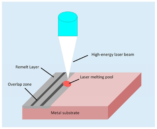
Figure 1.
Schematic diagram of laser surface melting processing process.
3. Discussion and Analysis
3.1. The Influence of Laser Parameters on the Surface Morphology
3.1.1. The Effect of Laser Frequency on the Surface Morphology
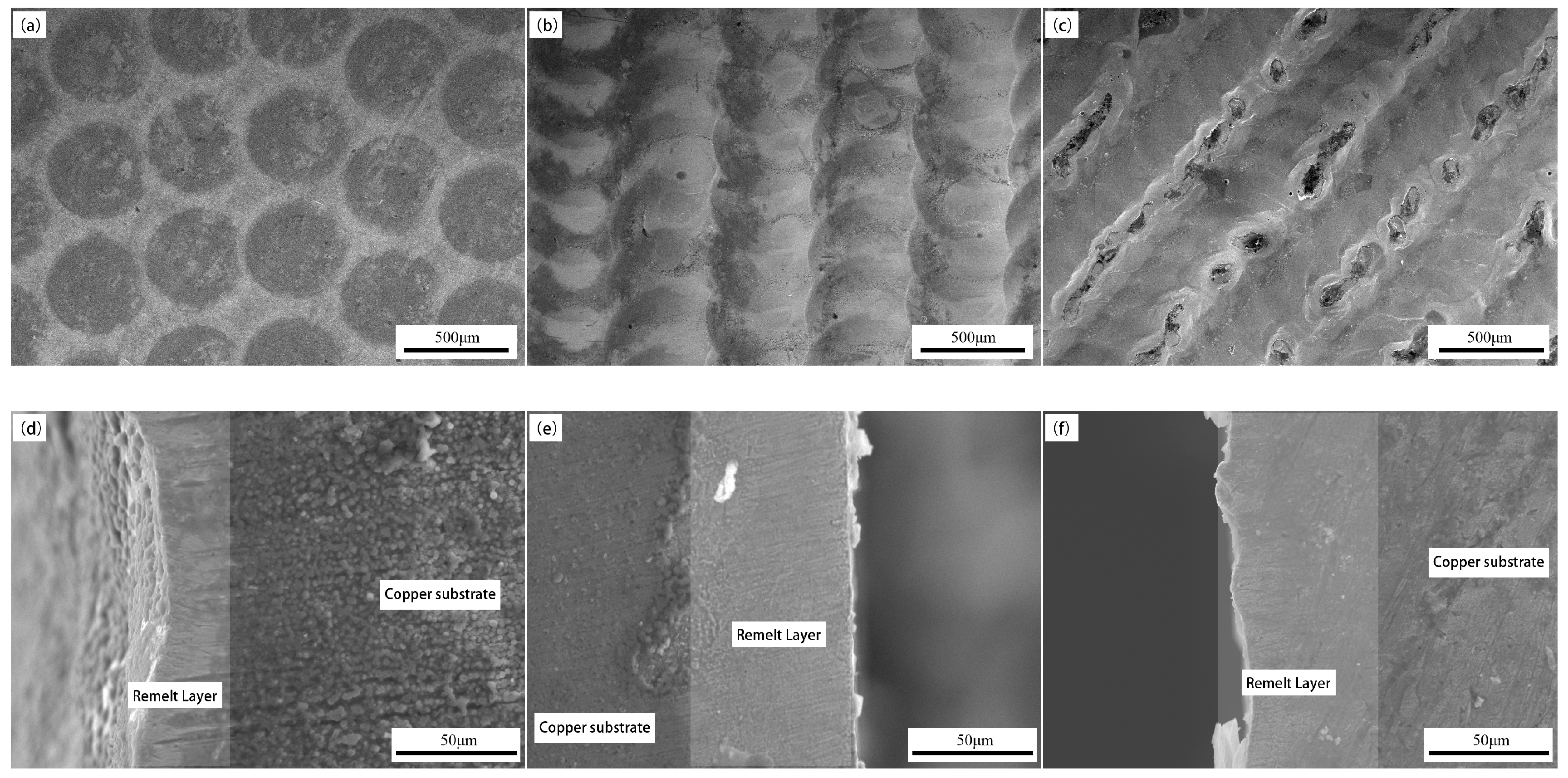
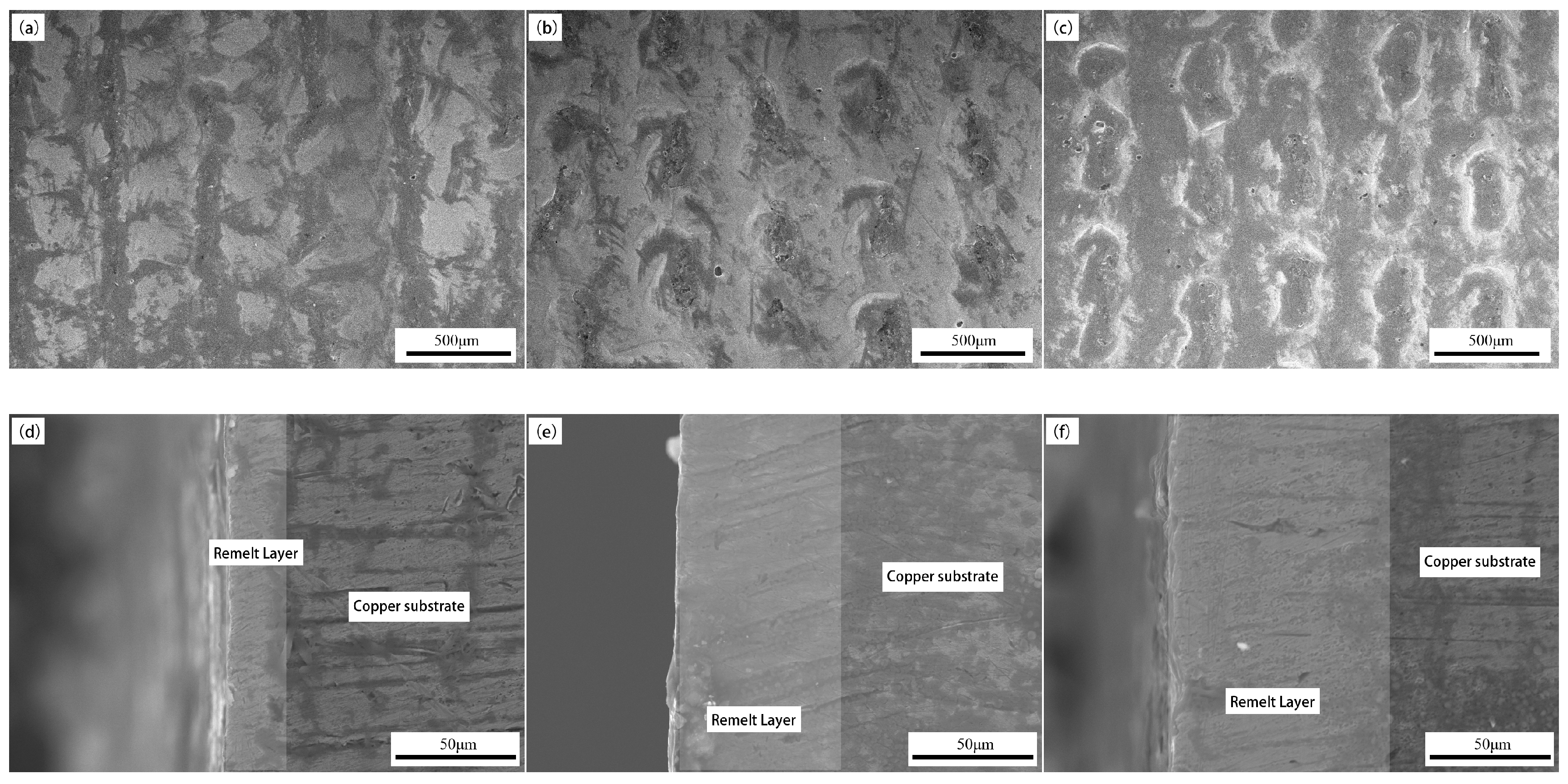
Figure 2 shows the surface and cross-sectional morphology of the sample when the energy density is kept at 132.69 J/mm2 and the pulse width is kept constant for 10 ms, and the laser pulse frequency is changed separately. As shown in Figure 2a, when the pulse frequency is 5 Hz, the laser generates regular molten spots on the copper surface, but the overall number of molten spots is relatively small, and the separation between the molten spots leads to the presence of untreated areas. When the pulse frequency is 10 Hz (Figure 2b), the surface of the sample presents a continuous strip of molten spots. The overlapping of the melting spots presents a fish scale-like hierarchical structure as a whole. The surface of the sample is flat and completely covered by the molten spot. When the pulse frequency is 15 Hz (Figure 2c), there are obvious banded pits on the sample surface, the outline of the circular melt spot becomes blurred, and the hierarchical structure of fish scales disappears. Comparing Figure 2d–f, it can be seen that when the frequency is 5 Hz, the thickness of the remelted layer is relatively thin, about 20 μm. When the pulse frequency is 10 Hz and 15 Hz, the thickness of the remelted layer increases to about 30 μm, but the thickness of the remelted layer of the sample is more uniform at 10 Hz.

Figure 2.
Surface and cross-sectional morphology of samples under different laser frequencies: (a,d) 5 Hz, (b,e) 10 Hz, (c,f) 15 Hz.
The change in surface morphology of the sample is mainly caused by the mismatch between feed rate and pulse frequency during the machining process. At the same feed rate, when the pulse frequency is 5 Hz, a lower pulse frequency will result in an insufficient number of laser remelting points generated per unit time, which cannot fully cover the feed path. When the pulse frequency is 15 Hz, there are too many remelting points generated on the surface of the sample per unit time, resulting in insufficient time and position intervals between adjacent melt spots, leading to repeated remelting.
3.1.2. The Effect of Pulse Width on the Surface Morphology
Figure 3 shows the surface and cross-sectional morphology of the sample when the laser energy density is kept at 132.69 J/mm2 and the pulse frequency is kept constant at 10 Hz, and the laser pulse width is changed separately. Compared to Figure 2b, when the pulse width is 7.5 ms (Figure 3a), the area of a single melt spot on the sample surface is small and the contour is unclear, and the overlapping area between the melt spots is small. The adjacent columns were not completely overlapped, and the surface coverage of the sample was not complete enough. When the pulse width increased to 12.5 ms (Figure 3b), molten pits with a diameter close to 200 μm appeared on the sample surface, and the pits remained relatively independent. The flatness of the sample surface decreases and the contour of the melt spot disappears. When the pulse width increases to 15 ms (Figure 3c), the size of the molten pits further increases, and there is a phenomenon of connectivity between adjacent molten pits, resulting in a further decrease in surface flatness. By comparing Figure 3d–f, it can be seen that as the pulse width gradually increases, the thickness of the remelted layer gradually increases from 15 μm to around 65 μm.
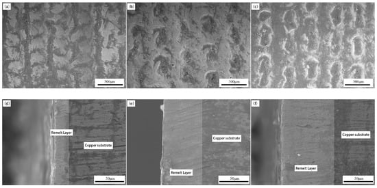
Figure 3.
Surface and cross-sectional morphology of samples under different laser pulse widths: (a,d) 7.5 ms, (b,e) 12.5 ms, (c,f) 15 ms.
The main reason for the above phenomenon may be due to the influence of pulse width on laser remelting energy. When the laser pulse width is 7.5 ms, the energy received by a single remelting point is lower, resulting in insufficient temperature rise at the remelting point and poor fluidity of the melt spot. When the laser pulse width is 12.5 ms, the energy of a single laser pulse is relatively high, and the temperature rise at the remelting point is too high. The molten material at the center of the melt pool is splashed by the impact, resulting in more obvious melt pits on the sample surface. When the laser pulse width increases to 15 ms, the energy received at the remelting point is greater, the temperature rise at the center of the molten pool intensifies, and the loss of molten material increases, leading to the connection of the molten pool.
3.1.3. The Effect of Laser Energy Density on the Surface Morphology
Figure 4 shows the surface and cross-sectional morphology of the sample when the energy density is changed separately under the condition of a laser pulse frequency of 10 Hz and a pulse width of 10 ms. From the figure, it can be seen that when the energy density is 99.52 J/mm2 (Figure 4a), the surface melt spots of the sample exhibit a regular fish scale-like hierarchical structure. However, compared to the surface morphology of 132.69 J/mm2 (Figure 2b), the overlapping area between adjacent molten spots on the sample surface is slightly smaller, and the circular contour of the molten spots is not clear enough. When the energy density is 165.87 J/mm2 (Figure 4b), a bamboo-like structure is formed on the sample surface along the feed direction, and the circular contour of the melt spot at the impact point basically disappears. There is a rope-like protrusion between adjacent columns of impact points. When the energy density increases to 199.04 J/mm2 (Figure 4c), compared with Figure 4b, the bamboo-like structure on the surface of the sample still exists, but the rope-like protrusions between adjacent rows of impact points are more obvious. Comparing Figure 2e and Figure 4d–f, it can be seen that the sample cross-section has good integrity and density. The thickness value of the remelted layer shows a gradually increasing trend as the laser energy density gradually increases, with its size increasing from 25 μm to around 50 μm.
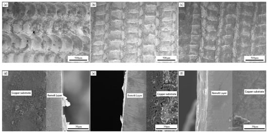
Figure 4.
Surface and cross-sectional morphology of samples under different energy density: (a,d) 99.52 J/mm2, (b,e) 165.87 J/mm2, (c,f) 199.04 J/mm2.
The reason for the above phenomenon may be that when the energy density is 99.52 J/mm2, the energy of the laser beam is lower, the temperature rise at the impact point is insufficient, and the fluidity of the molten material on the material surface is poor. When the energy density continues to increase from 132.69 J/mm2, the higher-energy laser beam significantly increases the temperature rise at the impact point. When the next melt spot is generated, the previous melt spot is still in a molten state. The interaction between the two adjacent points during the flow of molten material results in a bamboo-like morphology.
3.2. The Influence of Laser Parameters on the Surface Microhardness
3.2.1. The Effect of Laser Frequency on Surface Microhardness
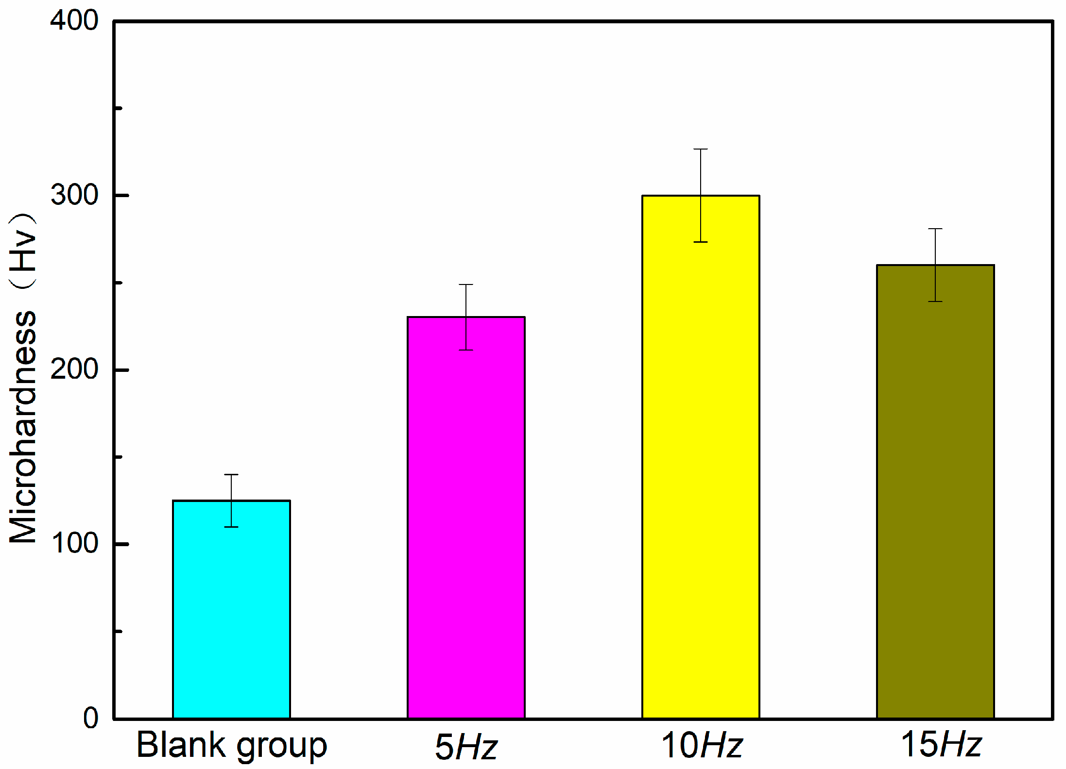
Figure 5 shows the microhardness values of the blank group and samples at different pulse frequencies. From the figure, it can be seen that the microhardness of the sample before laser treatment is about 125 Hv. Compared to the microhardness values of the blank group, the microhardness of the sample surface after laser remelting was significantly improved. The microhardness values of the sample surface at pulse frequencies of 5 Hz, 10 Hz, and 15 Hz are 230 Hv, 300 Hv, and 260 Hv, respectively. Among them, when the pulse frequency is 10 Hz, the microhardness value increases by 185, and the surface strengthening effect is significant. As the pulse frequency increases, the surface hardness value of the sample shows a trend of first increasing and then decreasing.

Figure 5.
Microhardness of the blank group and samples at different pulse frequencies.
The increase in surface microhardness of the sample is caused by the quenching hardening effect of the high-energy laser beam on the remelting point. The sharp rise and fall in temperature at the remelting point can refine the grain size of the material, generate beneficial stress on the material surface, and thereby improve the surface strength of the material [20,21]. When the laser frequency is low, the surface remelting point coverage of the sample is incomplete, resulting in a relatively low average microhardness on its surface. When the laser frequency is too high, the same remelting point is subjected to multiple pulse laser beams for a short period of time, resulting in an increase in defects such as pits and pores in the surface strengthening layer, and a decrease in microhardness value.
3.2.2. The Effect of Pulse Width on Surface Microhardness
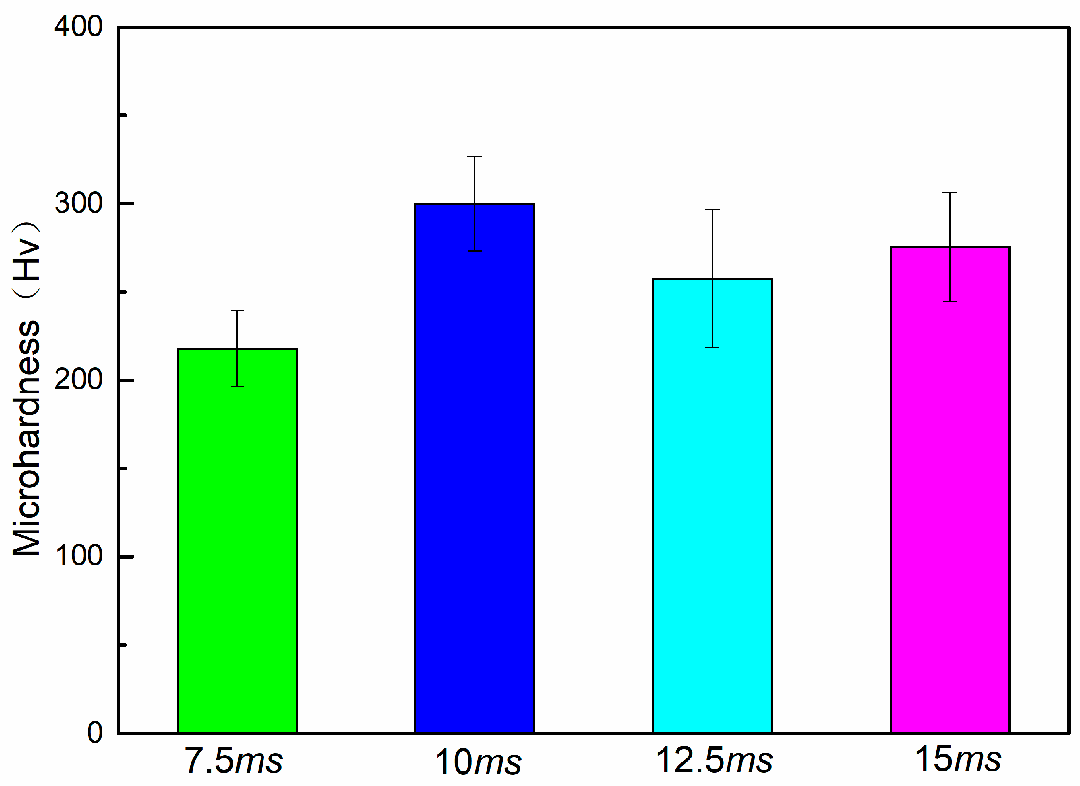
Figure 6 shows the microhardness values of the samples under different laser pulse width parameters. From the graph, it can be seen that as the pulse frequency gradually increases, the microhardness of the sample shows a slight fluctuation, but overall shows a trend of first increasing and then decreasing. The microhardness values are 218 Hv, 300 Hv, 257 Hv, and 276 Hv, respectively. Compared to the blank group, the microhardness values of the samples increased by 93, 175, 133, and 151 under different pulse width laser treatment parameters, respectively. It is worth noting that, under the premise that the sample surface is covered by remelting points, the microhardness value increases by 82 when the pulse width parameter increases from 7.5 ms to 10 ms. When the pulse width increased from 10 ms to 12.5 ms, the microhardness value decreased by 43. The microhardness value of the sample showed a significant change.

Figure 6.
Microhardness of the samples under different laser pulse widths.
The above changes in microhardness values may be due to the fact that as the pulse width increases from 7.5 ms to 10 ms, the laser remelting intensity on the sample surface gradually increases, and the thickness and uniformity of the remelted layer are improved, resulting in a gradual increase in microhardness. When the pulse is 12.5 ms, a higher laser intensity causes splashing of the molten material during the strengthening process, resulting in a lower thickness of the molten layer and more structural defects. When the pulse width increases to 15 ms, the increased laser intensity further intensifies the splashing phenomenon of molten material, but its melting depth on the surface of the sample also increases. At the depth of the molten layer, there are relatively fewer structural defects in the material, resulting in a slight increase in microhardness. It can also be inferred from the significant changes in microhardness values that the microhardness of the sample is more sensitive to changes in laser pulse width parameters.
3.2.3. The Effect of Energy Density on Surface Microhardness
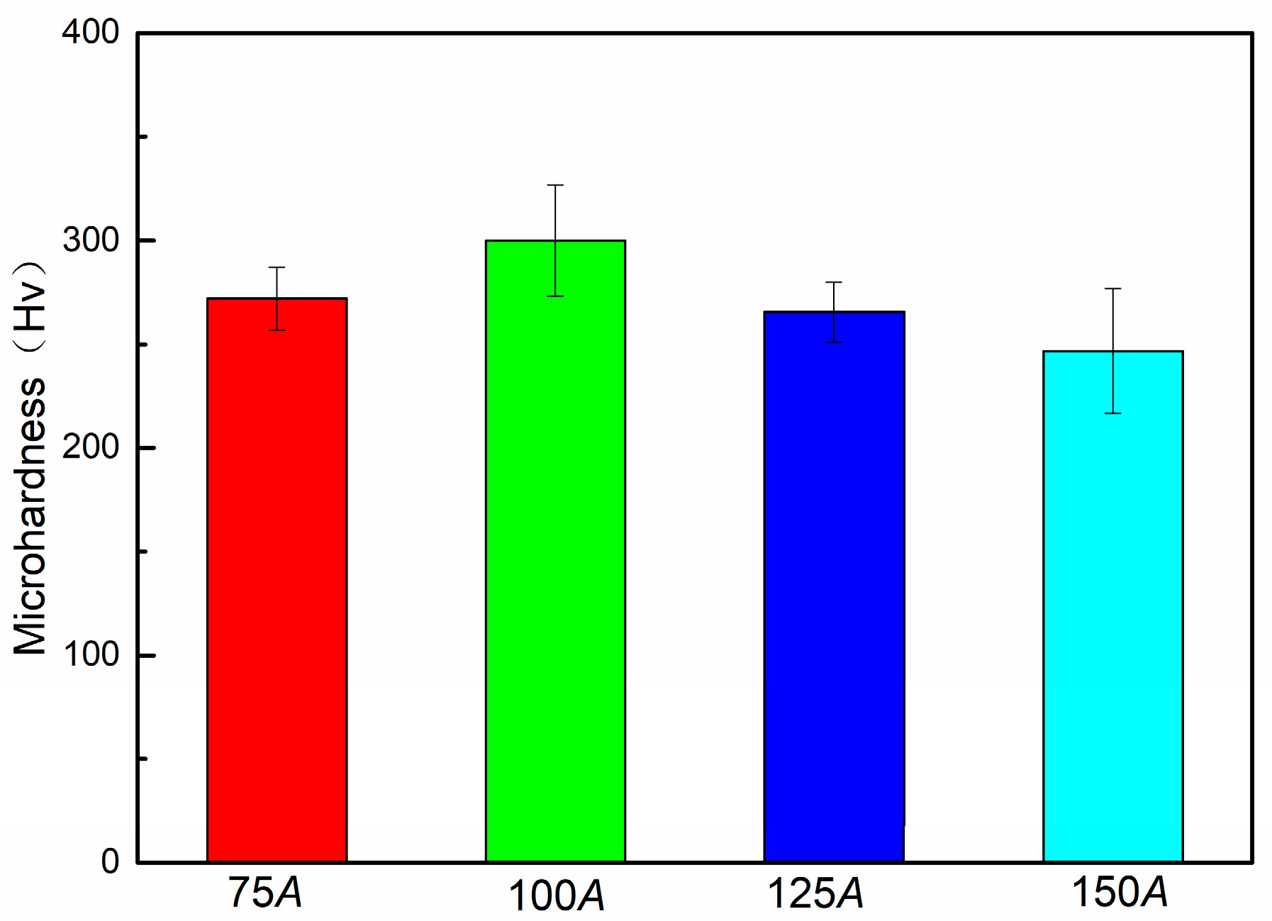
Figure 7 shows the microhardness of the sample surface under different laser energy density. From the graph, it can be seen that as the laser energy density increases, the overall microhardness value of the sample shows a small trend of first increasing and then decreasing, with microhardness values of 272 Hv, 300 Hv, 266 Hv, and 247 Hv, respectively. When the energy density increases from 99.52 J/mm2 to 199.04 J/mm2, its effect on the surface microhardness of the sample is relatively small compared to the microhardness under different frequency and pulse width parameters. Based on the surface morphology of samples under different energy density, the reason for this phenomenon may be that the changes in energy density only slightly alter the morphology of the remelted layer on the sample surface, without causing significant damage to the remelted layer. A relatively complete and regular remelting layer can reduce the number of structural defects such as pores and trachoma in the material, resulting in a relatively stable range of microhardness changes in the sample.
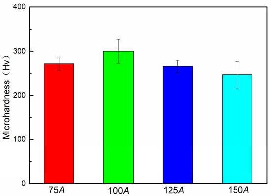
Figure 7.
Microhardness of the samples under different energy density.
3.3. The Influence of Laser Parameters on the Surface Wear Resistance
3.3.1. The Effect of Laser Frequency on the Surface Wear Resistance
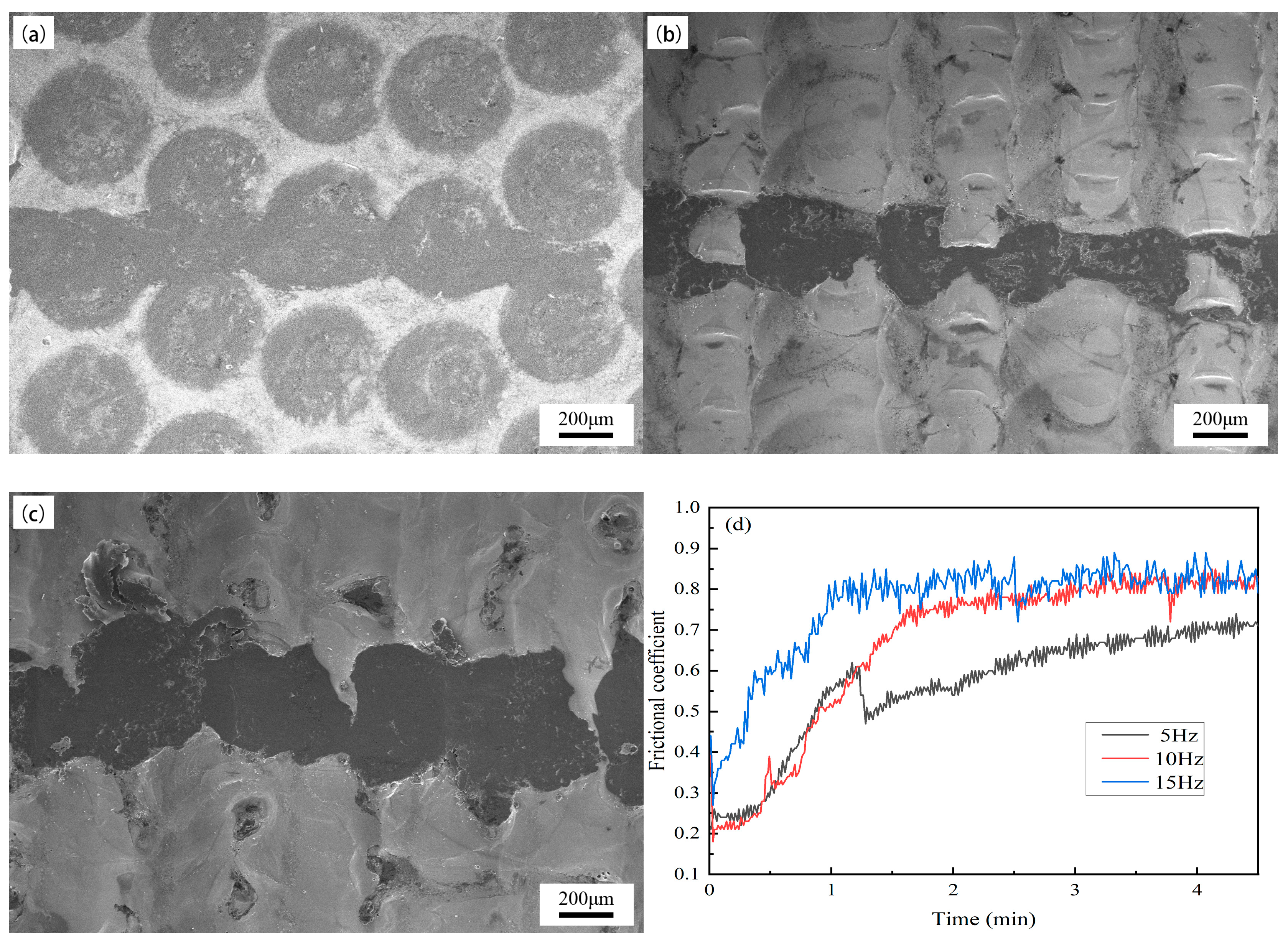
Figure 8 shows the surface morphology and friction curve of the worn samples under different frequencies. By comparing the wear marks in Figure 8a–c, it can be seen that the wear form on the sample surface is adhesive wear. As the laser frequency increases, the degree of wear on the sample surface first decreases and then increases. When the frequency is 5 Hz, the sample surface presents relatively uniform strip-like abrasions, with a width of approximately 260 μm. When the frequency increases to 10 Hz and 15 Hz, the wear marks of the sample surface are gourd-shaped. The widest point is located at the overlapping position between adjacent columns, with a width of approximately 230 μm and 490 μm. The narrow point is located at the center of the same column, with a width of approximately 120 μm and 200 μm.
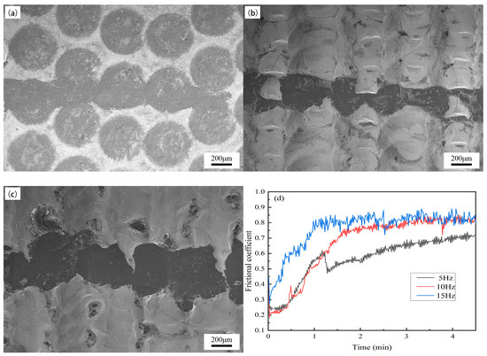
Figure 8.
Surface morphology and friction curve of the worn samples under different frequencies: (a) 5 Hz, (b) 10 Hz, (c) 15 Hz, (d) friction curve.
Based on the analysis of the wear curve in Figure 8d, the change in the shape of the wear mark is mainly caused by the change in the microhardness value. When the frequency is low, the molten spots at the impact point do not overlap, and the strengthening layer on the surface is thin and incomplete. After wearing of short duration, the strengthening layer is completely destroyed, resulting in more uniform wear marks. As the frequency increases, the molten spots between the impact points overlap. However, during the laser progressive scanning process, the time interval between adjacent columns of melting points is greater than the time interval in the same column. A larger time interval can lead to insufficient bonding strength of the stacked parts, resulting in gourd-shaped grinding marks.
3.3.2. The Effect of Pulse Width on the Surface Wear Resistance
Figure 9 shows the surface morphology and friction curve of the worn samples under different pulse width parameters. From the figure, it can be seen that as the pulse width increases, the gourd-shaped wear marks on the sample surface gradually disappear and transform into a straight line. When the pulse width is 7.5 ms, there are multiple continuous strengthening layers after wear, and the remelted layer is not completely worn. When the pulse width is 12.5 ms, the width of the wear marks is large, and the remelted layer is almost completely lost. When the pulse width continued to increase to 15 ms, compared to Figure 9b, the overall width of the wear marks slightly decreased. The phenomenon of spalling of the remelted layer is observed in both Figure 9b,c.
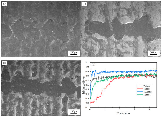
Figure 9.
Surface morphology and friction curve of the worn samples under different pulse widths: (a) 7.5 ms, (b) 12.5 ms, (c) 15 ms, (d) friction curve.
From the previous analysis of microhardness, it can be seen that the change in surface morphology at the worn area is mainly caused by the influence of pulse width on the microhardness. It is worth noting that although the microhardness value of the sample with a pulse width of 15 ms is greater than the microhardness value of 12.5 ms, in the friction curve (Figure 9d), the friction coefficient of the 12.5 ms sample is lower than that of the 15 ms sample. Based on the analysis of the surface morphology mentioned earlier, the abnormal changes in the friction curve may be caused by changes in the surface flatness of the sample.
3.3.3. The Effect of Laser Energy Density on the Surface Wear Resistance
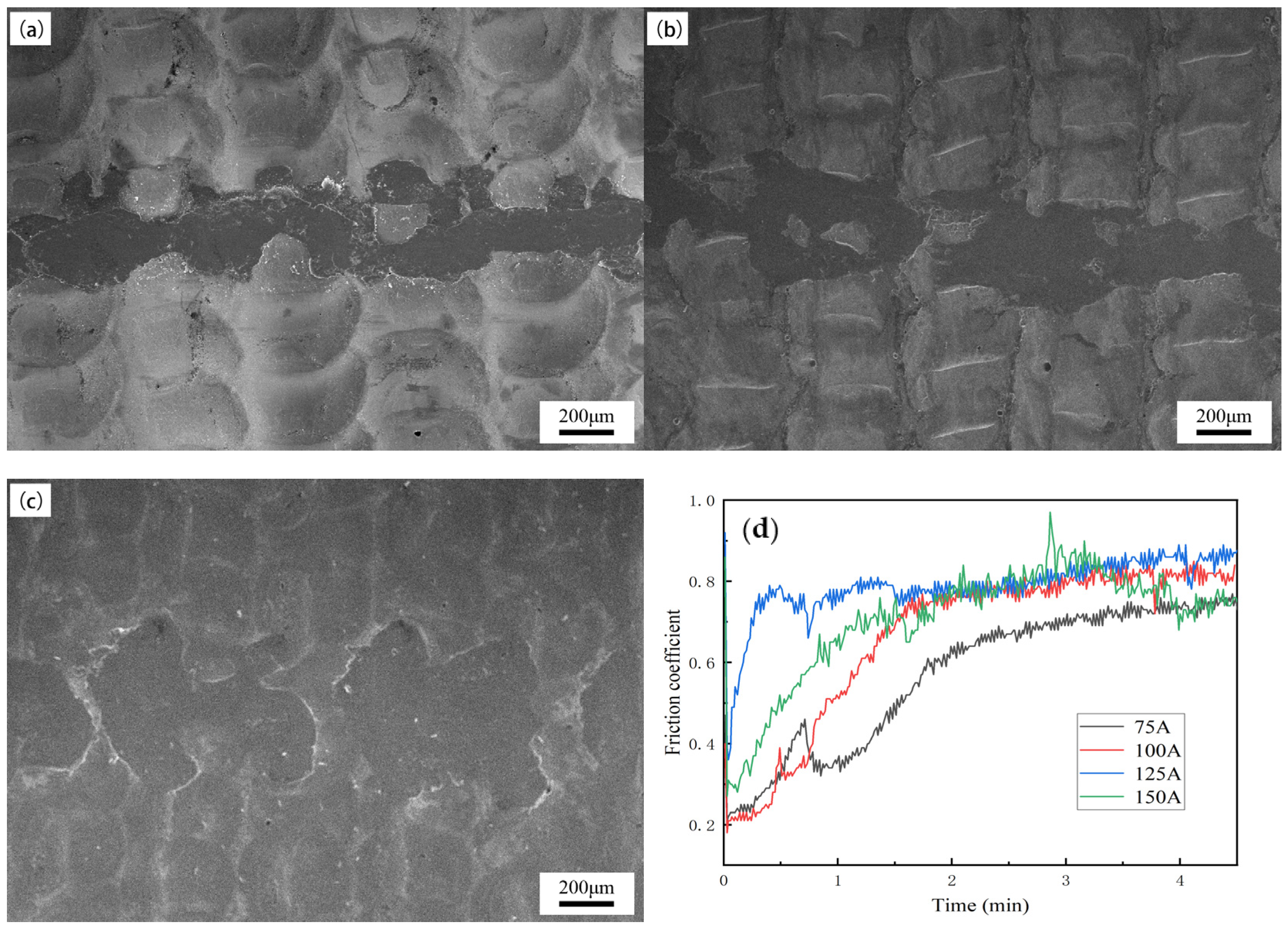
Figure 10 shows the surface morphology and friction curve of the worn samples under different energy density. From the figure, it can be seen that there is a partially remelted layer remaining on the worn surface of the sample. Compared to the surface morphology of the worn sample at 132.69 J/mm2, the wear width of the samples increases slightly when the energy density is 99.52 J/mm2 and 165.87 J/mm2, with an average value of about 180 μm and 220 μm, respectively. When the energy density is 199.04 J/mm2, the wear width of the sample further increases, with an average value of about 400 μm. The change in wear width of the sample is mainly due to the different microhardness values of the samples.
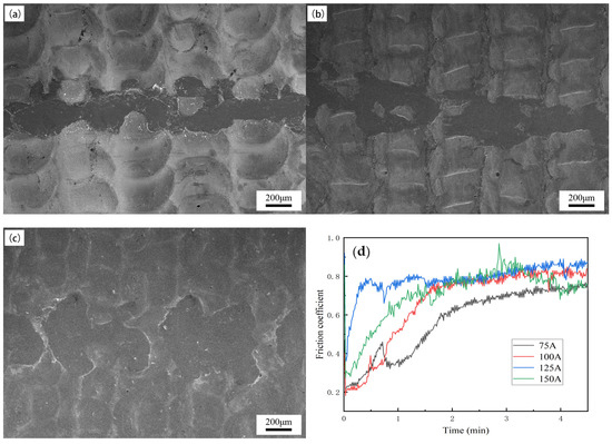
Figure 10.
Surface morphology and friction curve of the worn samples under different energy density: (a) 99.52 J/mm2, (b) 165.87 J/mm2, (c) 199.04 J/mm2, (d) friction curve.
From the friction curve of the sample, it can be seen that when the energy density is 99.52 J/mm2, the friction coefficient of the sample is slightly lower than that of 132.69 J/mm2, which is due to the better surface flatness of the sample under this parameter. About 3 min after the start of the wear test, the friction curves of samples 165.87 J/mm2 and 199.04 J/mm2 intersect, and the main reason for this phenomenon may be the change in surface flatness at the wear marks of the two samples.
4. Conclusions
This article aims to improve the surface wear resistance of copper contacts in high-voltage switches, and studies and analyzes the effects of laser frequency, pulse width, and energy density parameters on the surface morphology, microhardness, and wear resistance of copper during the laser surface remelting process. The research results indicate that the above process parameters can directly affect the wear resistance of the samples, but their influencing mechanisms are different. The effect of laser frequency on wear resistance is caused by the variation in the superposition relationship between impact points. The influence of pulse width and energy density on wear resistance is caused by changes in laser intensity at the impact point, and the changes in microhardness are more sensitive to pulse width. The results of the wear test are basically consistent with the trend of microhardness changes, but the surface flatness of the sample after remelting has a certain impact on the test curve during its wear process. When the pulse frequency is 10 Hz, the pulse width is 10 ms, and the pulse energy density is 132.69 J/mm2, the sample exhibits a more balanced surface morphology, microhardness, and wear resistance.
Author Contributions
Conceptualization, H.L.; methodology, H.L.; software, Y.C. and S.C.; validation, Y.C. and Z.T.; formal analysis, Y.C. and Z.T.; investigation, H.L.; resources, C.L.; data curation, H.L. and C.L.; writing—original draft preparation, Y.C.; writing—review and editing, Y.C. and S.C.; visualization, C.L.; supervision, H.L.; project administration, H.L.; funding acquisition, H.L. All authors have read and agreed to the published version of the manuscript.
Funding
This research was funded by the Scientific Research Foundation for Doctoral of Suzhou University (Suzhou University: 2020BS009), Anhui Province Excellent Talent Support Program for Universities (Anhui Provincial Department of Education: gxyq2020059), the Natural Science Research Project in Universities of Anhui Province in China (Anhui Provincial Department of Education: 2022AH051386, 2023AH010055), Anhui Higher Education Quality Engineering Project (Anhui Provincial Department of Education: 2022jyxm1595, 2020gnxm070, 2021jyxm1502, 2020mooc566).
Institutional Review Board Statement
Not applicable for studies not involving humans or animals.
Informed Consent Statement
Not applicable.
Data Availability Statement
Data are contained within the article.
Conflicts of Interest
The authors declare no conflict of interest.
References
- Gao, M.Y.; Xie, H.B.; Fang, Y.T.; Wang, H.T.; Liu, J.B. Progress in surface treatment techniques of copper and copper alloys. Chin. J. Nonferrous Met. 2021, 31, 1121–1133. [Google Scholar]
- Chen, C.; Guo, Z.H.; Guo, Y.Y.; Wang, R.Z.; Tang, E.L. Variable mechanism of electrical impedance for MCT high voltage switch under synergetic action of the mechanical and electric loads. Phys. Scr. 2023, 98, 105977. [Google Scholar] [CrossRef]
- Miao, J.; Chen, P.; Wu, J.F.; Fei, B.; Wu, X.; Liu, W.; Wan, J.F.; Wang, Y. Multi-spectral Characteristics of Arc Discharge in Switch Cabinet. J. Phys. Conf. Ser. 2022, 2359, 012005. [Google Scholar] [CrossRef]
- Yang, B.K.; Chen, Y.; Hao, W.K.; Han, Y.; Zhang, Q.; Li, Y.J.; Wang, X.F.; Huang, L.Y.; Lu, Y.L. The Corrosion Behavior of Different Silver Plating Layers as Electrical Contact Materials in Sulfur-Containing Environments. Coatings 2023, 13, 1796. [Google Scholar] [CrossRef]
- Ni, Y.Q.; Dong, G.N.; Tong, Z.; Li, X.; Wang, W. Effect of laser remelting on tribological properties of Babbitt alloy. Mater. Res. Express 2019, 6, 096570. [Google Scholar] [CrossRef]
- Zhu, J.; Hua, Y.T.; He, Q.S.; Liu, Y.; Huang, A.J.; Yang, Y.; Zhang, K. Research Progress on Laser Remelting in Selective Laser Melting. Rare Met. Mater. Eng. 2023, 52, 1932–1942. [Google Scholar]
- Wang, F.; Zuo, H.; Zhao, L.; Chen, M. Surface Quality and Property of Copper Treated by Laser Shock Peening. Prog. Laser Electron. 2017, 54, 041410. [Google Scholar] [CrossRef]
- Feng, Y.Y.; Ye, Y.X.; Lian, Z.C.; Xuan, T.D. Experimental Research on Effect of Surface Quality of Copper Treated by Laser Shock Peening. Laser Optoelectron. Prog. 2015, 52, 198–204. [Google Scholar]
- Liu, X.P.; Zhang, P.L.; Lu, Y.L.; Yan, H.; Lu, Z.S. Study on Tribological Properties of Ni-Based Silicide Coating on Copper by Laser Cladding. Chin. J. Lasers 2015, 42, 232–238. [Google Scholar]
- Li, K.; Fang, J.H.; Liao, R.B.; Jiang, Y.H.; Xu, J.; Li, J.Y.; Cao, H.J.; Luo, T.M.; Zhang, J. Research Status and Prospect of High-performance Metal Laser energy-field Surface Heat Treatment Technology. Chin. J. Lasers 2024, 4, 1–30. Available online: http://kns.cnki.net/kcms/detail/31.1339.TN.20231114.1007.032.html (accessed on 15 November 2023).
- Li, C.W.; Zhu, J.L.; Cai, Z.L.; Mei, L.; Jiao, X.D.; Du, X.; Wang, K. Microstructure and Corrosion Resistance of Underwater Laser Cladded Duplex Stainless Steel Coating after Underwater Laser Remelting Processing. Materials 2021, 14, 4965. [Google Scholar] [CrossRef]
- Xie, H.B.; Guan, W.M.; Lv, H.; Yang, H.Y.; Gao, M.Y.; Fang, Y.T.; Liu, J.B.; Wang, H.T. W-Cu/Cu composite electrodes fabricated via laser surface alloying. Mater. Charact. 2022, 185, 111715. [Google Scholar] [CrossRef]
- Zhang, B.; Wang, H.M.; Chen, R.; He, B.; Cao, Y.G.; Liu, D. Laser surface alloying with carbon on 15-5PH steel for improved wear resistance. Surf. Eng. 2021, 37, 669–677. [Google Scholar] [CrossRef]
- He, J.Y.; Wu, X.Q.; Xie, F.Q.; Dong, M.J.; Zhou, K.; Li, L.; He, D.D.; Wang, S.Q. Microstructure and Wear Properties of Laser Remelted Microarc Oxide Coating on Titanium Alloy. Rare Met. Mater. Eng. 2023, 52, 2424–2433. [Google Scholar]
- Xiong, T.C.; Yin, Y.Y.; Lu, D.H.; Wu, G.L.; Wang, Y.; Yao, J.H. Microstructure and Mechanism of Copper Layer Processed with Laser Remelting and Electrochemical Deposition Interaction Process. Chin. J. Lasers 2023, 50, 67–79. [Google Scholar]
- Zheng, Z.J.; Zheng, X. Temperature field simulation and process optimization of SLM forming of 316L stainless steel based on laser remelting. Mater. Rep. 2024, 38, 1–12. Available online: http://kns.cnki.net/kcms/detail/50.1078.TB.20230824.1109.002.html (accessed on 15 November 2023).
- Xiong, A.H.; Liu, Y.H.; Li, K.; Zhang, H.Y.; Fu, J.Y. Numerical Simulation and Experiments of Gray Cast Iron by Laser Surface Remelting. Laser Optoelectron. Prog. 2022, 59, 247–256. [Google Scholar]
- Liu, R.; Yu, J.C.; Yang, Q.F.; Wu, Z.J.; Xi, M.Z.; Gao, S.Y. Effect of Laser Power on Mechanical Property and Strengthening Mechanism of DH36 Marine Steel. Surf. Technol. 2023, 52, 408–417. [Google Scholar]
- Li, P.; Kong, L.H.; Huang, X.; Lian, G.F.; Yang, J.W. Corrosion Resistance of Stainless-Steel Surface Based on Laser Remelting. Spec. Cast. Nonferrous Alloys 2021, 41, 995–1000. [Google Scholar]
- Zhang, P.; Zhou, H.; Wang, C.T.; Liu, Y.; Ren, L.Q. Wear properties of H13 with micron scale and nano scale grains bionic units processed by laser remelting. Optics Laser Technol. 2013, 54, 219–224. [Google Scholar] [CrossRef]
- Amaya-Vázquez, M.R.; Sánchez-Amaya, J.M.; Boukha, Z.; El Amrani, K.; Francisco, J.B. Application of Laser Remelting Treatments to Improve the Properties of Ti6Al4V Alloy. Mater. Sci. Forum 2012, 1646, 25–30. [Google Scholar] [CrossRef]


Disclaimer/Publisher’s Note: The statements, opinions and data contained in all publications are solely those of the individual author(s) and contributor(s) and not of MDPI and/or the editor(s). MDPI and/or the editor(s) disclaim responsibility for any injury to people or property resulting from any ideas, methods, instructions or products referred to in the content. |
© 2023 by the authors. Licensee MDPI, Basel, Switzerland. This article is an open access article distributed under the terms and conditions of the Creative Commons Attribution (CC BY) license (https://creativecommons.org/licenses/by/4.0/).