Article

Influence of the Annealing Environment on the Structure and Ferroelectric Properties of Lead Titanate Thin Films

by
Aleksandras Iljinas
,
Vytautas Stankus
and
Liutauras Marcinauskas
*
Department of Physics, Kaunas University of Technology, Studentu Str. 50, LT-51368 Kaunas, Lithuania
*
Author to whom correspondence should be addressed.
Coatings 2024, 14(1), 58; https://doi.org/10.3390/coatings14010058
Submission received: 25 November 2023 / Revised: 19 December 2023 / Accepted: 27 December 2023 / Published: 30 December 2023

Abstract

:
Lead titanate thin films of pyrochlore phase were deposited using layer-by-layer reactive magnetron sputtering on a heated platinized silicon substrate. It was found that the pyrochlore phase transition to the perovskite phase was initiated at 700 °C, and the properties of the PbTiO3 films could be controlled by changing the annealing environment. The thin films annealed in air and oxygen environments (1.33 Pa) have a tetragonal structure. The highest values of remnant polarization and the coercive field were 38 μC/cm2 and 130 kV/cm, respectively, but the largest dielectric loss was determined for the films annealed in air. The remnant polarization, coercive field and dielectric loss were reduced when the annealing of films was performed using oxygen gas at 1.33 Pa pressure. The films annealed in vacuum showed a rhombohedral (and ferroelectric) structure with the lowest remnant polarization and coercive field values. Such a structure was not observed for lead titanate at room temperature. It was observed that the surface morphology strongly depended on the reaction rate, which was influenced by the oxygen concentration in the environment.

1. Introduction

Ferroelectric materials and thin films are widely used in broad application areas such as actuators, transducers, ferroelectric random-access memories (FeRAMs), pyroelectric sensors, energy storage capacitors, solar cells, etc. [1,2,3,4,5,6,7,8,9,10]. Lead titanate (PbTiO3) is a well- known perovskite-type structure of ferroelectric material due to its unique ferroelectric, piezoelectric and pyroelectric properties [4,11,12]. Bulk ceramics of lead titanate are already used in many devices. Meanwhile, PbTiO3 thin films are a very perspective material and have great potential for use in electronics devices, such as pyroelectric infrared detectors [5,6], capacitors [7], ultrasonic transducers [8], microsensors, actuators [9] and nonvolatile memories (FRAMs) [4,5,6,7,8]. Ferroelectric memories are one of the most promising technologies of future memories. Perovskite-type lead titanate has a high Curie temperature (490 °C), large tetragonality (c/a = 1.063), relatively low permittivity, a large pyroelectric coefficient and easy spontaneous polarization [4,9,10,13]. These films are still under intense research due to their unique properties. PbTiO3 films, as with other ferroelectric films, have been synthesized by many physical and chemical methods [10,13,14,15,16]. Many of them have not yet solved the problem of a dense, well-ordered crystal structure and the required or controlled stoichiometry films. The buffer layers, such as SrRuO3, SrTiO3, etc., are used in growing lead titanate thin films. These buffer layers provide the required lattice match and promote formation of the desirable crystallographic orientation of PbTiO3 films [2,15]. Some methods report lead loss in high temperature substrates [17], cracks in the microstructure [18], stoichiometry problems [19] and nonuniformity of the film surface.
Pulse laser deposition enables precise control of the growth rate to deposit dense, high purity thin ferroelectric films with the required composition. However, the use equipment is expensive, and to obtain the desirable film composition, an adapted target composition is required [15,16]. Magnetron sputtering is one of the most prospective methods for PbTiO3 thin film formation because of its high deposition rate, the possibility of using commercially available large area deposition systems, the control of the substrate temperature during the deposition and the relatively low cost [12,15,17,20,21,22,23,24].
R. Nishino et al. [15] investigated thin PbTiO3 films synthesized using pulsed laser deposition and discovered that the remnant polarization depended on the thickness of the PbTiO3 films. Y. Fu et al. [25] found that the low thermal conductivity of PbTiO3 is due to the presence of low frequency optical phonons associated with the polar modes. F. Zhang et al. [26] observed that the increase in the axial ratio (c/a from 1.1 to 1.45) of supertetragonal perovskites induces a large polarization due to the coupling between the unit cell and ion displacements, which results in better ferroelectric properties. Y. Feng et al. [27] showed that the increase in thickness of the PbTiO3 films enlarges the width of the stripe domains. J. Sakai et al. [16] found that the phase structure and ferroelectric properties of the PbTiO3 films prepared using pulsed laser deposition depended on the used areal ratios of the PbO:TiO2 target. H. W. Shin et al. [28] observed that the ferroelectric properties, c/a ratio and the leakage current characteristics of the PbTiO3 films were enhanced with the increase in the band gap values from 3.8 eV to 4.0 eV. H. El Hosiny Ali et al. [14] demonstrated that the crystallinity and ferroelectric properties of the lead titanate films strongly depend on the annealing temperature. O. Azaroual et al. [29] found that the PbTiO3 films deposited using the sol–gel technique and annealed at 650 °C showed a remnant polarization of 18 μC/cm2 and coercive field of 121 kV/cm. Our previous studies [20,21,22] demonstrated that the phase structure, surface morphology and ferroelectric properties of the PbTiO3 films strongly depended on the substrate temperature or postdeposition annealing conditions. It was observed that the c/a ratio and crystallite size of the PbTiO3 films annealed at 770 oC depend on the Pb/Ti ratio [21]. The PbTiO3 films formed in situ on the hot substrates (temperature varied from 450 to 550 °C) showed a remnant polarization of 60 μC/cm2 and coercive field of 150 kV/cm [20]. The structure and ferroelectric properties of PbTiO3 films annealed in air at various temperatures are studied the most [14,17,29]. It should be noted that there is a lack of research that allows us to compare the structure and properties of lead titanate thin films annealed in various environments.
The aim of this work was to synthesize lead titanate thin films using layer-by-layer reactive magnetron sputtering at a substrate temperature of 400 °C and to investigate the influence of the postannealing environments on the structural and ferroelectric properties.

2. Materials and Methods

The lead titanate oxide thin films were deposited on platinized silicon substrate using reactive magnetron layer-by-layer deposition in O2 gas environment (p = 1.33 Pa). The purity of the oxygen gas used for the formation of the films and postannealing was 99.999%. Multilayer system Pt/Ti/SiO2/Si was used as substrate, with a thickness of Pt, TiO2 and SiO2 layer of 200 nm, 50 nm and 1 µm, respectively. The SiO2 thin film on Si (100) substrate was grown using thermal oxidation method. The Pt and TiO2 layers deposited using magnetron sputtering at room temperature were (111) oriented. The deposition of lead titanate was realized using substrate periodic and parallel to cathode motion over the magnetrons (layer by layer). The period of motion was 3 s. Pb and Ti disc targets of 3 inches in diameter (from Kurt. J. Lesker Company, Jefferson Hills, PA, USA, purity 99.95%) were used. The distance between magnetrons and substrate was kept at 65 mm. The Ti and Pb target currents were fixed at 1.0 A and 0.3 A, respectively. The samples were heated during this magnetron deposition at 400 °C. TiO2 and PbO deposition rates were constant (8 nm/min and 9 nm/min, respectively). The total time of deposition process was 30 min. The total thickness was chosen and determined as 0.50 ± 0.01 µm. The thickness was determined using Linnic micro-interferometer and tested with profilometer (Ambios XP-200 Profiler, Ambios Technology Inc., Santa Cruz, CA, USA). The changes in crystallo-graphic composition and surface properties of the deposited film structures were investigated after annealing process for one hour at 700 °C in air, O2 gas environment (p = 1.33 Pa) and vacuum (p = 5 × 10⁻³ Pa).
The films were analyzed using scanning electron microscope (SEM) (RAITH-e-LiNE, Raith GmbH, Dortmund, Germany). The SEM images of the thin films were captured at 10,000 (for surface) and 20,000 (for cross-section) magnifications and using acceleration voltage of 10 kV. Working distance was changed from 6 mm to 10 mm, depending on the analyzed film. The gun vacuum was ~1.9 × 10⁻⁷ Pa, and system vacuum was ~5.8 × 10⁻⁴ Pa during the measurements. The crystallographic structure of thin films was investigated using X-ray diffraction (XRD) (Bruker D8 series diffractometer, Bruker AXS from GmbH, Bruker Corporation, Billerica, MA, USA) using 40 kV, 30 mA, monochromatic Cu Kα radiation (λ = 1.5405 Å), with a scan speed of 2θ = 5 min−1 in the scan range from 20° to 60° 2θ using Bragg–Brentano geometry. The average size of crystallites of thin films was determined from the peak broadening using single line and multiple line analysis. The peaks were analyzed using WinFit software (Version 1.2, 1996.), and the average size of thin film crystallites was determined from the peak broadening by the single line and multiple line analyses and was checked using the Scherrer equation:
D = K λ β cos θ
where D is the mean crystallite size, λ is diffraction wavelength, β is the line broadening at full width at half maximum after subtracting the instrumental line broadening, θ is the diffraction angle, and K is a dimensionless shape factor, with a value close to unity. The shape factor of 0.9 was used.
The top electrodes used to perform traditional ferroelectric measurements (creating a capacitor structure) were deposited using aluminum thermal evaporation through a mask. The electrode matrix consisted of 5–10 disk-shaped electrodes (thickness ~100 nm, surface area ~1.23 mm2). Polarization dependence on the electric field strength (P-E loop measurements) was performed by means of the Sawyer and Tower method by supplying the created capacitor structure with up to 50 V AC sine voltages. The frequency was kept at 50 Hz during the measurements [30]. Multifunctional data acquisition (DAQ) NI USB-6361 device (National Instruments Corporation, Austin, TX, USA.) was used for faster scientific research and analysis.

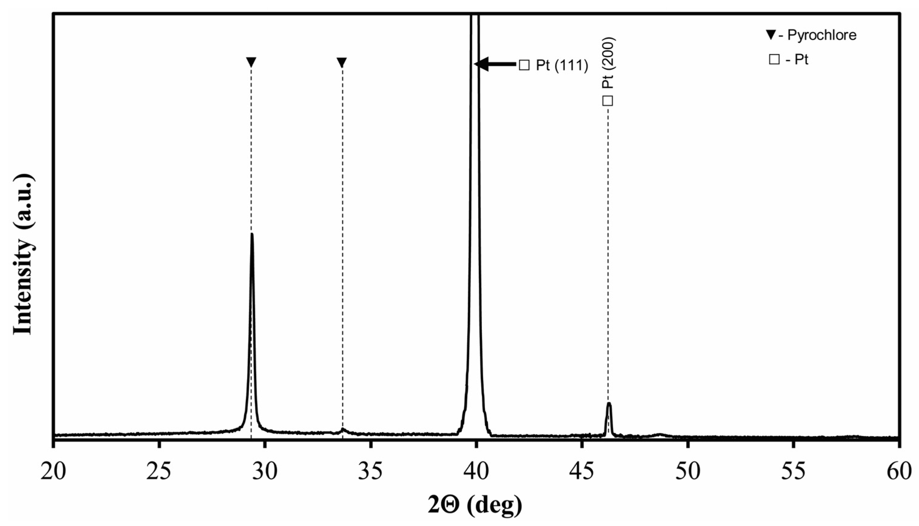
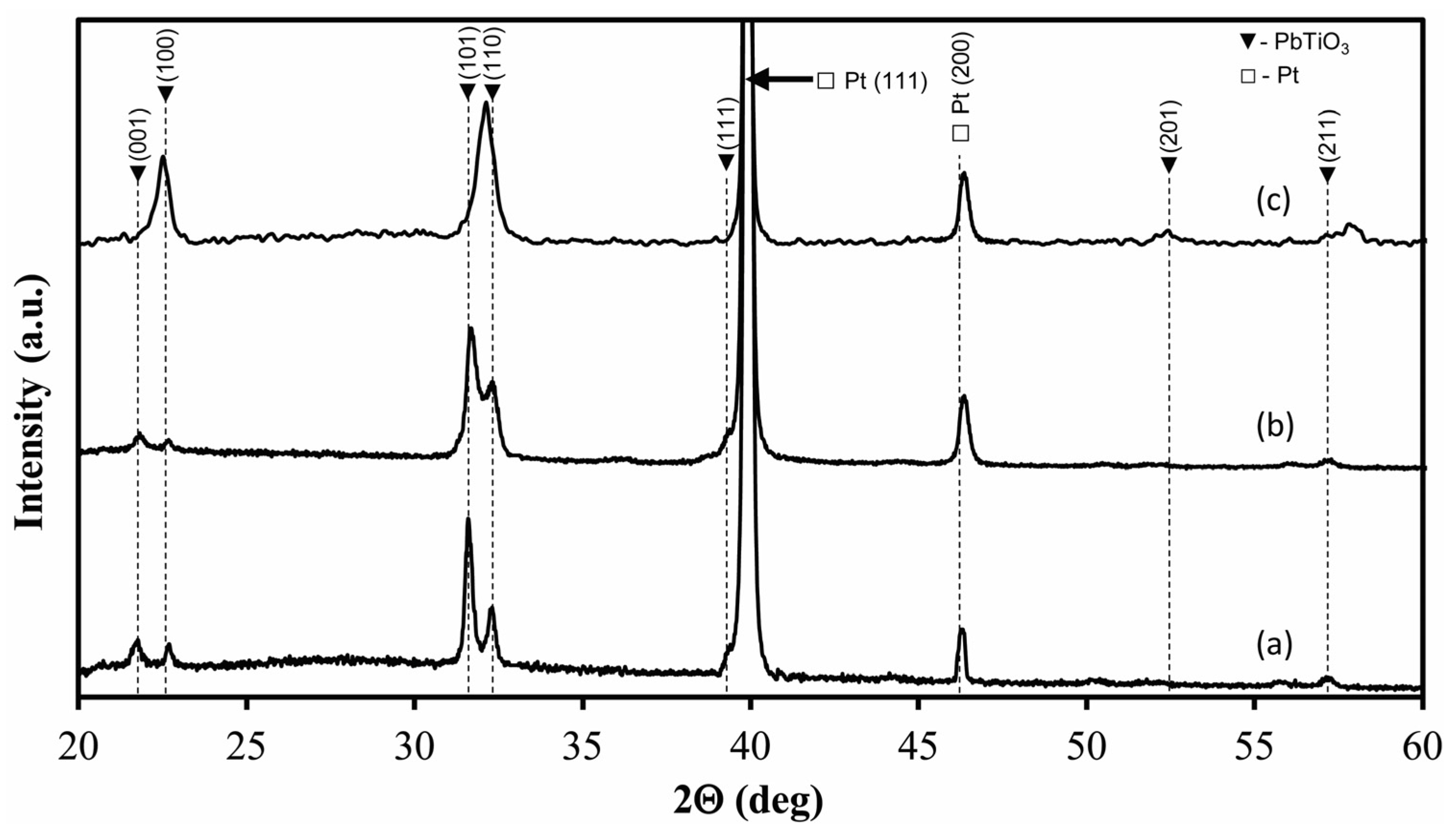
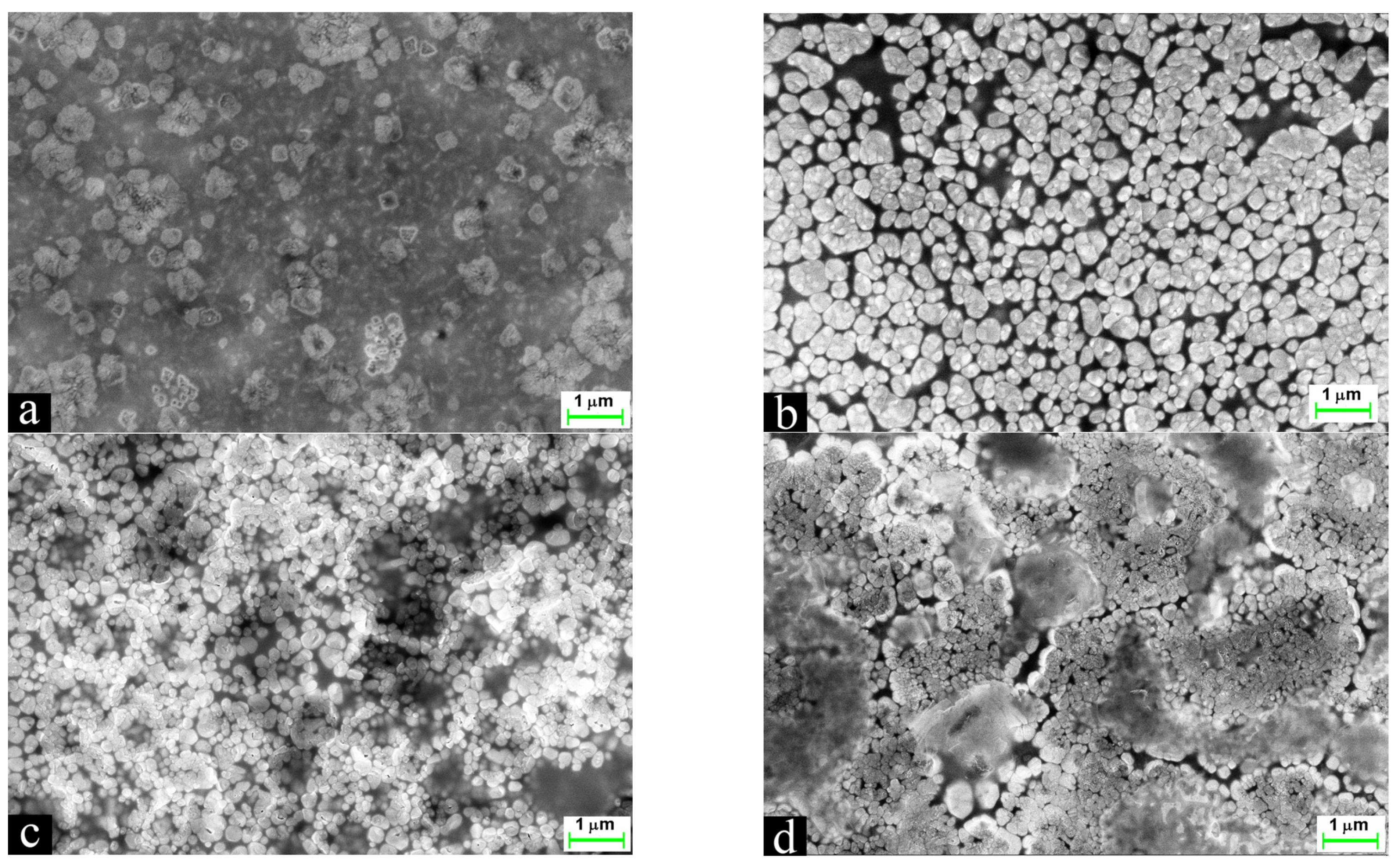
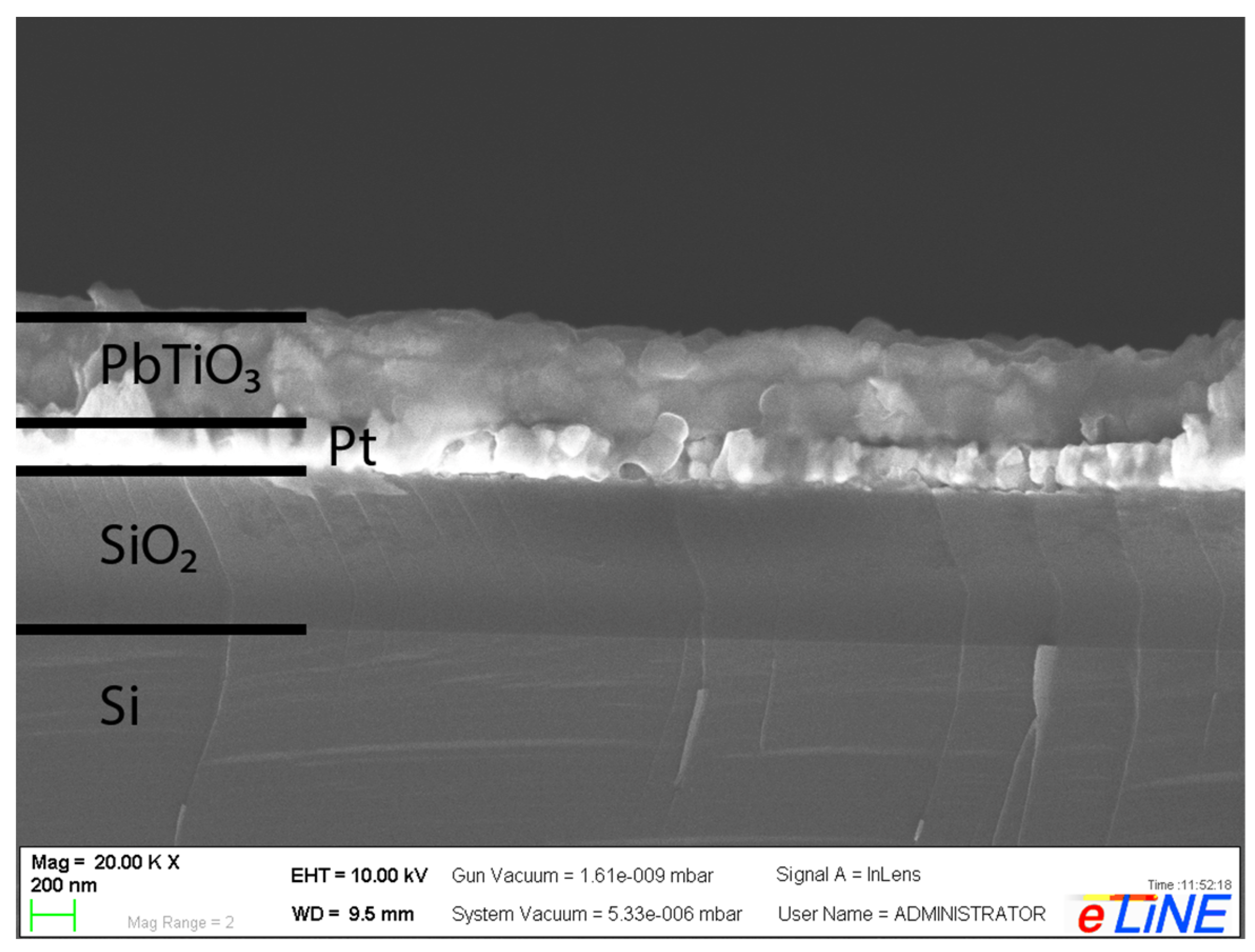
3. Results and Discussion

It should be noted that the crystalline nature of PbTiO3 thin films strongly depends on the substrate material and the substrate temperature when films are grown using direct current magnetron sputtering [20,22]. A silicon substrate does not fit for lead titanate formation because of the large lattice mismatch between Si and lead titanate. A platinum coating was used as a buffer layer and as a metallic electrode between PbTiO3 and Ti/SiO2/Si, as lead titanate and Pt have lattice mismatches only of 0.5% [13]. The XRD patterns of sputtered thin film are given in Figure 1. The high intensity peak at ~29.34° and low intensity peak at 34.05° are attributed to the lead titanate pyrochlore (Pb2Ti2O6) phase (Figure 1). The nonferroelectric pyrochlore phase Pb2Ti2O6 is the metastable polymorph of the perovskite phase [11,31]. These results indicate that the 400 °C substrate temperature is too low for the direct formation of the PbTiO3 perovskite phase during film growth. It was found that the lead titanate films pyrolyzed at 250 °C, 300 °C and 400 °C demonstrate mixed pyrochlore and perovskite phases [11]. Several authors [14,32] indicated that 400 °C is the lowest temperature observed for the crystallization of PbTiO3 thin films.
The lead titanate films were postannealed at 700 °C temperatures for one hour in different environments in order to induce a phase transition and produce a tetragonal perovskite phase in the deposited films. The XRD patterns of lead titanate films annealed in different environments are presented in Figure 2. The presence of a pure PbTiO3 perovskite phase was observed for all annealed thin films. The highest intensity peak at ~39.9° was assigned to the platinum (111) planes due to the used buffer layer. The peaks at 2θ = 21.78°, 22.72°, 31.59°, 32.29°, 39.59° and 57.22° were assigned to the (001), (100), (101), (110), (111) and (211) PbTiO3 planes, respectively [20]. The appearance of these peaks indicates formation of the tetragonal PbTiO3 phase in the film [14,18,32]. The dominant peak in the film annealed in air was related to the (101) plane. Signals of the PbTiO3 (111) planes were of a low intensity and overlapped with the peak attributed to the platinum for the films annealed in air and oxygen environments. The main reason could be due to the contrast of the recording not being sufficiently high to resolve the smaller top layer reflection in the immediate vicinity of the broad Pt substrate signal. The film annealed in the oxygen gas environment demonstrated the same peaks attributed to the tetragonal PbTiO3 phase (Figure 2b). However, the intensity of the peak related to the (110) plane was enhanced, while the intensity of the peak attributed to the (100) plane was reduced (Figure 2b).
The XRD measurements clearly indicated that the postannealing at various environments affected the crystalline structure and lattice type of the PbTiO3 films. The main differences were found in the crystal structure, crystallite sizes and tetragonality. The thin films annealed in air exhibit the tetragonal phase, with the largest lattice spacing “c”–to “a” ratio or c/a = 1.042 and are close to the bulk c/a value [33] (Figure 2a). The crystallite size was determined as 26 nm. Our previous investigations [21] indicated that the c/a ratio was 1.047, and the average crystallite size was 65 nm when the PbTiO3 films were annealed at 770 °C in air. Different results were obtained after annealing as-deposited film in an oxygen environment at 1.33 Pa pressure (Figure 2b). The tetragonality of the lattice space was reduced to 1.039. The crystallite size slightly decreased to 23 nm. The higher c/a ratio in the PbTiO3 films usually leads to better ferroelectric properties [28]. H.E.H Ali et al. [14] demonstrated that the c/a ratio of the lead titanate films was reduced from 1.052 to 1.044 with the increase in the temperature from 400 to 650 °C. It was found that a deficiency of lead in the composition of PbTiO3 films does not lead to the formation of the perovskite phase, even after annealing at 700 °C [34].
It should be noted that annealing in vacuum had a totally different effect on the crystalline structure of the formed PbTiO3 film compared to films annealed in air or using an oxygen gas environment. The XRD patterns shown in Figure 2c do not match with the tetragonal PbTiO3 phase but show a similarity with the rhombohedral (ferroelectric) or cubic (paraelectric) structure [35] of PbTiO3. The (101) peak is almost merged with the stronger (110) peak occurring on the lower 2θ angle position (32.15°). The peak of the (001) plane obtained in the films annealed in air and oxygen also merged. The broad and high intensity peak appeared at 22.54°. This effect was observed in perovskite solid solutions such as PZT [36,37], PMN-PT [38], PIN–PT [39] and NBT [40] but was never observed in PbTiO3. The lead titanate perovskite phase at room temperature typically exists in a tetragonal crystal structure [33,41,42] but exhibits a cubic structure above the Curie temperature (490 °C) [42]. We discovered that annealing in vacuum resulted in the transition of the pyrochlore phase not to a tetragonal but to a rhombohedral or cubic structure, and the induced phase was stable at room temperature. The formation of the rhombohedral phase was observed in the BiScO3–PbTiO3 ceramics when the lowest fraction of PbTiO3 was used. The increase in the concentration of PbTiO3 led to the transition from the rhombohedral to the tetragonal phase [43]. We think that it happens because of lattice deformation due to oxygen atom deficiency. This deficiency already exists in the previous (pyrochlore) phase. It means that additional oxygen atoms are needed to form the tetragonal perovskite structure during annealing and phase transformation. Very low covalency of Pb–O bonds [44], interruption of these bonds during annealing at a high temperature and evaporation of oxygen atoms can also influence this process. But it did not happen when the films were annealed in oxygen or air environments. The crystallite size of the film annealed in vacuum was determined as 20 nm.
Hysteresis loops of the polarization of each film as a function of applied voltage were measured at 1 kHz (Figure 3). All postannealed films exhibit ferroelectric properties, with different coercive fields, remnant polarizations and hysteresis areas (Table 1). The highest values of polarization (38 μC/cm2) and coercive field (130 kV/cm) were determined in the film annealed in air. The highest area shows the largest dielectric loss there is in the films. The annealing of the film in the oxygen reduced the polarization value to 20 μC/cm2 and the coercive field to 70 kV/cm, respectively. These values are smaller, but the dielectric loss was also reduced. The lowest polarization and coercive field values were obtained after annealing the film in vacuum. The polarization was only ~7 μC/cm2, which was more than five times lower compared to the film annealed in air. The coercive field was 30 kV/cm. Although these values are minimal, the thin film exhibits slight ferroelectric properties. Therefore, based on the weak ferroelectric properties, we can assume that the crystal structure of thin film annealed in vacuum is not cubic but rhombohedral. It should be noted that the P-E loops of all annealed films demonstrated a slightly higher negative voltage than the positive voltage values (Figure 3). Strong asymmetric polarization hysteresis curves were observed in lead zirconate titanate ceramics [44]. The authors indicated that such an effect is due to a unipolar polarization orientation. The shift in electric field is attributed to a domain pinning effect caused by defects existing in the structure [45,46]. It was demonstrated that the domain pinning could be reduced when measurements are performed at a higher temperature. The rearrangement of defects with the ferroelectric polarization at a higher temperature is stipulated, and freeze-in upon cooling resulted in a stabilized polarization [44].
Figure 4 shows the SEM images of thin films deposited and annealed in different environments. The deposited pyrochlore film has a dense structure with some defects (Figure 4a). Various irregular shape grains with size ranking from 200 nm up to 1 µm were formed. The morphology of thin film drastically changes after annealing due to recrystallization-induced phase transition. Granular or most likely agglomerated structures of (200–800 nm) sizes were obtained after annealing of the film in air. As it was seen, these grains are separated by gaps of various sizes. The postannealing of the film resulted in phase recrystallization from the pyrochlore to the perovskite phase. The remnants of the pyrochlore phase may be present, but the dark areas observed in the surface image are most likely attributed to voids or pores between the individual grain columns. Anyway, an XRD analysis did not show any pyrochlore phase remnants in the film annealed in air. An SEM cross-section was performed to answer this question.
The cross-section image of the film shows a dense structure with some voids (Figure 5). Therefore, we must presume that the dark areas in the surface images (Figure 4a) are indicating the existence of pores and voids but not remnants of the pyrochlore phase. Annealing in an oxygen environment (1.33 Pa) leads to the formation of a similar surface morphology, with a smaller size grain (100–500 nm) and more dense structure (Figure 4c). The film annealed in vacuum showed the smallest grained structure (50–300 nm), but the grains are grouped in a few micrometer-size blocks (Figure 4d). It is seen that oxygen concentration in an annealing environment affects the morphology of thin films differently. It is well known that the structure and morphology of lead titanate depends on the reaction rate from the pyrochlore to the perovskite phase [47].
J.I. Jang et al. [34] observed that significant lead excess in the composition of lead titanate films influenced the crystallization of the perovskite phase in the temperature range from 550 °C to 700 °C. However, the annealed films had a porous microstructure, apparently due to the loss of the excess PbO. L. Haimin et al. [48] found that 0.7 BiFeO3–0.3 PbTiO3 films annealed in air and O2 flow were fully crystallized and demonstrated the preferred (100) orientation. The addition of O2 gas was useful to prevent the generation of oxygen vacancies in the films. The crystallization and formation of the large size grains was observed after annealing PbTiO3 films at 650 °C [49].
Typically, the reaction rate depends on the temperature. In our case, the reaction rate is influenced by the oxygen concentration in the environment too. According to M. Avrami’s theory [50], the grain size depends on two factors: the initial nucleation center number growth rate and the phase grain growth rate. In our case, the increase in the oxygen concentration gives the increase in reaction rate from the pyrochlore to the perovskite phase, and it explains why the grain sizes (and crystallite size) are larger. On the other hand, the decrease in oxygen influences the growth of the large size nucleation centers and, therefore, the grain sizes (and the crystallites) were smaller. The postannealed PbTiO3 thin films had pores and voids, which could also affect the electric properties. Several authors indicated that porosity reduced the remnant polarization values of ferroelectric materials and thin films. The porous ceramic materials or films have a lower fraction of the active component compared to more dense materials and will have a smaller level of polarization [51,52,53]. The increase in the porosity also reduces the coercive field values in ceramics. The electric field distribution in dense materials or films is more homogeneous. Meanwhile, the permittivity of pores or voids is significantly lower. Thus, the applied electric field would be concentrated in the low permittivity region of pores. As a result, an inhomogeneous electric field distribution will be created throughout the film structure, leading to domain switching at different applied electric fields [52,53,54]. V. Stancu et al. [52] demonstrated that the porous Pb(Zr0.2Ti0.8)O3 films showed hysteresis loops, with remnant polarization values lower compared to the dense film. Additionally, it was stated that the asymmetry of the hysteresis loop and the leakage current increased with the porosity values. K.J. Kormandy et al. [54] indicated that the ferroelectric properties of the BaTiO3 films depended on the porosity and tetragonality values. The coercive field was higher for the dense films with higher tetragonality. The PbTiO3 film annealed at 500 °C had a higher c/a value and similar grain size but was less porous compared to the film annealed at 400 °C. It led to higher remnant polarization but lower coercive field values [14]. The PbTiO3 film annealed in air demonstrated the hysteresis loop shape closest to a rectangle. Such behavior could be due to faster polarization reversal related to the lower porosity values, highest crystallite sizes and tetragonality of the lattice space [28,33,52].

4. Conclusions

Lead titanate thin films were deposited using layer-by-layer reactive magnetron sputtering. The thin films deposited at 400 °C substrate temperatures demonstrated the lead titanate pyrochlore phase. Phase transitions from the PbTiO3 pyrochlore phase to the perovskite phase in the films were successfully initiated by a solid-state reaction in various environments by annealing at 700 °C for one hour. It was observed that the tetragonality, crystallite sizes and electrical properties of PbTiO3 films strongly depended on the annealing environment (oxygen content). The films annealed in air and oxygen (1.33 Pa) environments showed a tetragonal structure. The thin film annealed in vacuum showed the crystalline structure most likely attributed to the rhombohedral (ferroelectric) phase of lead titanate. The highest values of remnant polarization (38 μC/cm2) and coercive field (130 kV/cm) were determined for the film annealed in air due to the highest c/a ratio, the largest crystallites and the lowest porosity. After annealing the film in an oxygen environment, the remnant polarization decreased to 20 μC/cm2, and the coercive field decreased to 70 kV/cm, respectively. The lowest polarization and coercive field values were obtained for the film annealed in vacuum. The surface morphology strongly depended on the reaction rate influenced by the oxygen concentration in the environment. The largest grains were obtained in films annealed in air and the smallest in the PbTiO3 films annealed in vacuum.

Author Contributions

Conceptualization, A.I.; methodology, A.I. and V.S.; software, V.S.; validation, A.I. and V.S.; formal analysis, A.I., V.S. and L.M.; investigation, A.I. and V.S.; resources, A.I. and L.M.; data curation, A.I and V.S.; writing—original draft preparation, A.I., V.S. and L.M.; writing—review and editing, A.I., V.S. and L.M.; visualization, V.S.; supervision, V.S. and A.I. All authors have read and agreed to the published version of the manuscript.

Funding

This research received no external funding.

Institutional Review Board Statement

Not applicable.

Informed Consent Statement

Not applicable.

Data Availability Statement

Data are contained within the article.

Conflicts of Interest

The authors declare no conflicts of interest.

References

  1. Li, S.; Wang, Y.; Yang, M.; Miao, J.; Lin, K.; Li, Q.; Chen, X.; Deng, J.; Xing, X. Ferroelectric Thin Films: Performance Modulation and Application. Mater. Adv. 2022, 3, 5735–5752. [Google Scholar] [CrossRef]
  2. Martin, L.W.; Rappe, A.M. Thin-Film Ferroelectric Materials and Their Applications. Nat. Rev. Mater. 2016, 2, 16087. [Google Scholar] [CrossRef]
  3. Singh, R.; Tripathi, A.; Gautam, M. 23—Ferroelectric Perovskite Thin Films as Nonvolatile Computer Memories. In Perovskite Metal Oxides; Moharana, S., Badapanda, T., Satpathy, S.K., Mahaling, R.N., Kumar, R., Eds.; Elsevier: Amsterdam, The Netherlands, 2023; pp. 595–616. [Google Scholar] [CrossRef]
  4. Müller, M.; Efe, I.; Sarott, M.F.; Gradauskaite, E.; Trassin, M. Ferroelectric Thin Films for Oxide Electronics. ACS Appl. Electron. Mater. 2023, 5, 1314–1334. [Google Scholar] [CrossRef]
  5. Sun, L.L.; Tan, O.K.; Liu, W.G.; Zhu, W.G.; Yao, X. Poling of Multilayer Pb(Zr0.3Ti0.7)O3/PbTiO3 Thin Film for Pyroelectric Infrared Sensor Application. Infrared Phys. Technol. 2003, 44, 177–182. [Google Scholar] [CrossRef]
  6. Fang, B.; Qian, K.; Yuan, N.; Ding, J.; Zhao, X.; Luo, H. Large Pyroelectric Response of 0.8Pb(Mg1/3Nb2/3)O3–0.2PbTiO3 Ceramics Prepared by Reaction-Sintering Method. Mater. Lett. 2012, 84, 91–93. [Google Scholar] [CrossRef]
  7. Szwagierczak, D.; Kulawik, J. Thick Film Capacitors with Relaxor Dielectrics. J. Eur. Ceram. Soc. 2004, 24, 1979–1985. [Google Scholar] [CrossRef]
  8. Cochran, S. 1—Piezoelectricity and Basic Configurations for Piezoelectric Ultrasonic Transducers. In Ultrasonic Transducers; Nakamura, K., Ed.; Woodhead Publishing: Sawston, UK, 2012; pp. 3–35. [Google Scholar] [CrossRef]
  9. Muralt, P. Ferroelectric Thin Films for Micro-Sensors and Actuators: A Review. J. Micromech. Microeng. 2000, 10, 136. [Google Scholar] [CrossRef]
  10. Czekaj, D.; Jaszczyszyn, E.; Orkisz, T.; Kozielski, L.; Lisinska-Czekaj, A.; Federowicz, E.; Modelski, J. Synthesis and Basic Properties of Ferroelectric Thin Films. Methods Materials and Novel Applications. In Proceedings of the 2006 International Conference on Microwaves, Radar & Wireless Communications, Krakow, Poland, 22–24 May 2006; pp. 692–699. [Google Scholar]
  11. Lima, E.C.; Guerra, J.D.S.; Rodrigues, A.D.; Bernardi, M.I.B.; M’Peko, J.C.; Hernandes, A.C. Investigation of the Structural Properties of PbTiO3 thin films. In Proceedings of the 2021 IEEE International Symposium on Applications of Ferroelectrics (ISAF), Virtual, 16–21 May 2021; pp. 1–4. [Google Scholar]
  12. Luo, C.; Li, D.; Liu, J.; Ma, Z. Investigation of Dielectric Constant for PbTiO3 Film in THz Range. Ferroelectrics 2023, 613, 22–30. [Google Scholar] [CrossRef]
  13. Palkar, V.R.; Purandare, S.C.; Pinto, R. Ferroelectric Thin Films of PbTiO3 on Silicon. J. Phys. D Appl. Phys. 1999, 32, R1. [Google Scholar] [CrossRef]
  14. Ali, H.E.H.; Ricote, J.; Calzada, M.L.; Bretos, I.; Jiménez, R. The Influence of the Crystallization Temperature on the Reliability of PbTiO3 Thin Films Prepared by Chemical Solution Deposition. J. Eur. Ceram. Soc. 2017, 37, 1449–1458. [Google Scholar] [CrossRef]
  15. Nishino, R.; Fujita, T.C.; Kagawa, F.; Kawasaki, M. Evolution of Ferroelectricity in Ultrathin PbTiO3 Films as Revealed by Electric Double Layer Gating. Sci. Rep. 2020, 10, 10864. [Google Scholar] [CrossRef] [PubMed]
  16. Sakai, J.; Roque, J.M.; Vales-Castro, P.; Padilla-Pantoja, J.; Sauthier, G.; Santiso, J. Pulsed Laser Deposition of Epitaxial Non-Doped PbTiO3 Thin Films from PbO–TiO2 Mosaic Targets. Coatings 2021, 11, 662. [Google Scholar] [CrossRef]
  17. Basit, N.A.; Kim, H.K.; Blachere, J. Temperature Dependence of Lead Loss in R.F. Magnetron Sputtering of a Stoichiometric Pb(Zr,Ti)O3 Target. Thin Solid Film. 1997, 302, 155–161. [Google Scholar] [CrossRef]
  18. Pontes, F.M.; Rangel, J.H.G.; Leite, E.R.; Longo, E.; Varela, J.A.; Araújo, E.B.; Eiras, J.A. Low Temperature Synthesis and Electrical Properties of PbTiO3 Thin Films Prepared by the Polymeric Precursor Method. Thin Solid Film. 2000, 366, 232–236. [Google Scholar] [CrossRef]
  19. Harjuoja, J.; Kosola, A.; Putkonen, M.; Niinistö, L. Atomic Layer Deposition and Post-Deposition Annealing of PbTiO3 Thin Films. Thin Solid Film. 2006, 496, 346–352. [Google Scholar] [CrossRef]
  20. Iljinas, A.; Marcinauskas, L.; Stankus, V. In Situ Deposition of PbTiO3 Thin Films by Direct Current Reactive Magnetron Sputtering. Appl. Surf. Sci. 2016, 381, 6–11. [Google Scholar] [CrossRef]
  21. Iljinas, A.; Stankus, V.; Kaliasas, R. Synthesis of PbTiO3 Thin Films by Annealing Multilayer Oxide Structures in Vacuum. Acta Phys. Pol. A 2016, 129, 121–124. [Google Scholar] [CrossRef]
  22. Iljinas, A.; Stankus, V.; Čyvienė, J.; Abakevičienė, B. Formation of PbTiO3 Thin Films on Seed Layers Using DC Magnetron Layer-by-Layer Deposition. Vacuum 2015, 122, 310–313. [Google Scholar] [CrossRef]
  23. Wu, J.-G.; Zhu, J.-L.; Xiao, D.-Q.; Zhu, J.-G.; Tan, J.-Z.; Zhang, Q.-L. Preparation and Properties of PbTiO3/(Pb1−xLax)TiO3/PbTiO3 Multi-Layer Films by Rf Magnetron Sputtering. Ferroelectrics 2007, 357, 271–275. [Google Scholar] [CrossRef]
  24. Weymann, C.; Lichtensteiger, C.; Fernandez-Peña, S.; Cordero-Edwards, K.; Paruch, P. Improved Thin Film Growth Using Slow Kinetics Intermittent Sputtering. Appl. Surf. Sci. 2020, 516, 146077. [Google Scholar] [CrossRef]
  25. Fu, Y.; Singh, D.J. Thermal Conductivity of Perovskite KTaO3 and PbTiO3 from First Principles. Phys. Rev. Mater. 2018, 2, 094408. [Google Scholar] [CrossRef]
  26. Zhang, F.; Zhang, J.; Jing, H.; Li, Z.; Wang, D.; Jia, C.-L. Correlations between Polarization and Structural Information of Supertetragonal PbTiO3. Phys. Rev. B 2022, 105, 024106. [Google Scholar] [CrossRef]
  27. Feng, Y.; Tang, Y.; Ma, D.; Zhu, Y.; Zou, M.; Han, M.; Ma, J.; Ma, X. Thickness-Dependent Evolution of Piezoresponses and Stripe 90° Domains in (101)-Oriented Ferroelectric PbTiO3 Thin Films. ACS Appl. Mater. Interfaces 2018, 10, 24627–24637. [Google Scholar] [CrossRef] [PubMed]
  28. Shin, H.W.; Son, J.Y. Tetragonally Strained Crystal Structure and Ferroelectric Properties of Epitaxial PbTiO3 Thin Films Grown on Single-Crystal Rh Substrates. Mater. Chem. Phys. 2021, 264, 124477. [Google Scholar] [CrossRef]
  29. Azaroual, O.; El Hasnaoui, M.; Akharchach, B.; Narjis, A. Ferroelectric Properties and Structural Characterisation of Lead Titanate Thin Films Prepared by Polymeric Precursor Method. Adv. Mater. Process. Technol. 2022, 8, 3674–3684. [Google Scholar] [CrossRef]
  30. Beklešovas, B.; Iljinas, A.; Stankus, V.; Čyvienė, J.; Andrulevičius, M.; Ivanov, M.; Banys, J. Structural, Morphologic, and Ferroelectric Properties of PZT Films Deposited through Layer-by-Layer Reactive DC Magnetron Sputtering. Coatings 2022, 12, 717. [Google Scholar] [CrossRef]
  31. Banerjee, R.; Purandare, S.C.; Palkar, V.R.; Pinto, R. Effect of Silicon on the Microstructure of Pulsed Laser Ablated Ferroelectric PbTiO3 Thin Films. J. Phys. D Appl. Phys. 2001, 34, 1037. [Google Scholar] [CrossRef]
  32. Martín-Arbella, N.; Bretos, Í.; Jiménez, R.; Calzada, M.L.; Sirera, R. Photoactivation of Sol–Gel Precursors for the Low-Temperature Preparation of PbTiO3 Ferroelectric Thin Films. J. Am. Ceram. Soc. 2011, 94, 396–403. [Google Scholar] [CrossRef]
  33. Schulze, G.F.; Jona, F.; Shirane, G. Ferroelectric Crystals. 402 S. Oxford/London/New York/Paris 1962. Pergamon Press. Preis Geb. 84 S. Net. Z. Angew. Math. Mech. 1963, 43, 512. [Google Scholar] [CrossRef]
  34. Yang, J.I.; Welsh, A.; Sbrockey, N.M.; Tompa, G.S.; Polcawich, R.G.; Potrepka, D.M.; Trolier-McKinstry, S. Annealing Behavior and Electrical Properties of Atomic Layer Deposited PbTiO3 and PZT Films. J. Cryst. Growth 2018, 493, 45–50. [Google Scholar] [CrossRef]
  35. Kobertz, D.; Müller, M.; Molak, A. Vaporization and Caloric Studies on Lead Titanate. Calphad 2014, 46, 62–79. [Google Scholar] [CrossRef]
  36. Li, H.-L.; Zhang, Y.; Zhou, J.-J.; Zhang, X.-W.; Liu, H.; Fang, J.-Z. Phase Structure and Electrical Properties of xPZN–(1−x)PZT Piezoceramics near the Tetragonal/Rhombohedral Phase Boundary. Ceram. Int. 2015, 41, 4822–4828. [Google Scholar] [CrossRef]
  37. Oliveira, C.A.; Longo, E.; Varela, J.A.; Zaghete, M.A. Synthesis and Characterization of Lead Zirconate Titanate (PZT) Obtained by Two Chemical Methods. Ceram. Int. 2014, 40, 1717–1722. [Google Scholar] [CrossRef]
  38. Tipakontitikul, R.; Ananta, S.; Yimnirun, R. Phase Formation and Transitions in the Lead Magnesium Niobate–Lead Zirconate Titanate System. Curr. Appl. Phys. 2006, 6, 307–311. [Google Scholar] [CrossRef]
  39. Wongsaenmai, S.; Tan, X.; Ananta, S.; Yimnirun, R. Dielectric and Ferroelectric Properties of Fine Grains Pb(In1/2Nb1/2)O3–PbTiO3 Ceramics. J. Alloys Compd. 2008, 454, 331–339. [Google Scholar] [CrossRef]
  40. He, C.; Zhang, Y.; Sun, L.; Wang, J.; Wu, T.; Xu, F.; Du, C.; Zhu, K.; Liu, Y. Electrical and Optical Properties of Nd3+-Doped Na0.5Bi0.5TiO3 Ferroelectric Single Crystal. J. Phys. D Appl. Phys. 2013, 46, 245104. [Google Scholar] [CrossRef]
  41. Rujiwatra, A.; Jongphiphan, J.; Ananta, S. Stoichiometric Synthesis of Tetragonal Phase Pure Lead Titanate under Mild Chemical Conditions Employing NaOH and KOH. Mater. Lett. 2005, 59, 1871–1875. [Google Scholar] [CrossRef]
  42. Idrissi, H.; Aboujalil, A.; Deloume, J.P.; Fantozzi, G.; Durand, B. Molten Salt Prepared Lead Titanate: Powder Characterization, Sintering and Physical Properties. J. Eur. Ceram. Soc. 1999, 19, 1997–2004. [Google Scholar] [CrossRef]
  43. Chen, J.; Shi, H.; Liu, G.; Cheng, J.; Dong, S. Temperature Dependence of Dielectric, Piezoelectric and Elastic Properties of BiScO3–PbTiO3 High Temperature Ceramics with Morphotropic Phase Boundary (Mpb) Composition. J. Alloys Compd. 2012, 537, 280–285. [Google Scholar] [CrossRef]
  44. de Lazaro, S.; Longo, E.; Sambrano, J.R.; Beltrán, A. Structural and Electronic Properties of PbTiO3 slabs: A Dft Periodic Study. Surf. Sci. 2004, 552, 149–159. [Google Scholar] [CrossRef]
  45. Kamel, T.M.; de With, G. Poling of Hard Ferroelectric Pzt Ceramics. J. Eur. Ceram. Soc. 2008, 28, 1827–1838. [Google Scholar] [CrossRef]
  46. He, C.; Wang, Z.; Li, X.; Yang, X.; Long, X.; Ye, Z.-G. Self-Polarized High Piezoelectricity and Its Memory Effect in Ferroelectric Single Crystals. Acta Mater. 2017, 125, 498–505. [Google Scholar] [CrossRef]
  47. Stankus, V.; Dudonis, J.; Pranevicius, L.; Pranevičius, L.L.; Milcius, D.; Templier, C.; Riviere, J.P. On the Mechanism of Synthesis of PbTiO3 Thin Films by Thermal Annealing of Pb/Ti Layers in Air at Atmospheric Pressure. Thin Solid Film. 2003, 426, 78–84. [Google Scholar] [CrossRef]
  48. Haimin, L.; Chunli, Q.; Jianguo, Z.; Mingzhe, H.; Qingsong, Y. Effect of Different Annealing Atmosphere on Ferroelectric Properties of 0.7BiFeO3-0.3PbTiO3 Thin Films. Rare Met. Mater. Eng. 2016, 45, 1449–1454. [Google Scholar] [CrossRef]
  49. Hsu, M.-C.; Sun, Y.-M.; Leu, I.-C.; Hon, M.-H. Structural and Electrical Characterizations of PbTiO3 Thin Films Grown on LaNiO3-Buffered Pt/Ti/SiO2/Si Substrates by Liquid Phase Deposition. J. Electrochem. Soc. 2006, 153, F260. [Google Scholar] [CrossRef]
  50. Avrami, M. Granulation, Phase Change, and Microstructure Kinetics of Phase Change. III. J. Chem. Phys. 1941, 9, 177–184. [Google Scholar] [CrossRef]
  51. Castro, A.; Ferreira, P.; Rodriguez, B.J.; Vilarinho, P.M. The Role of Nanoporosity on the Local Piezo and Ferroelectric Properties of Lead Titanate Thin Films. J. Mater. Chem. C 2015, 3, 1035–1043. [Google Scholar] [CrossRef]
  52. Stancu, V.; Lisca, M.; Boerasu, I.; Pintilie, L.; Kosec, M. Effects of Porosity on Ferroelectric Properties of Pb(Zr0.2Ti0.8)O3 Films. Thin Solid Film. 2007, 515, 6557–6561. [Google Scholar] [CrossRef]
  53. Zhang, Y.; Roscow, J.; Lewis, R.; Khanbareh, H.; Topolov, V.Y.; Xie, M.; Bowen, C.R. Understanding the Effect of Porosity on the Polarisation-Field Response of Ferroelectric Materials. Acta Mater. 2018, 154, 100–112. [Google Scholar] [CrossRef]
  54. Kormondy, K.J.; Popoff, Y.; Sousa, M.; Eltes, F.; Caimi, D.; Rossell, M.D.; Fiebig, M.; Hoffmann, P.; Marchiori, C.; Reinke, M.; et al. Microstructure and Ferroelectricity of BaTiO3 thin Films on Si for Integrated Photonics. Nanotechnology 2017, 28, 075706. [Google Scholar] [CrossRef]
Figure 1. XRD diagrams of thin films deposited on platinized silicon substrate at 400 °C.
Coatings 14 00058 g001
Figure 2. XRD diagrams of thin films deposited on platinized silicon substrate at 400 °C and postannealed at 700 °C temperatures for one hour in: (a) air, (b) O2 gas environment, (c) vacuum.
Coatings 14 00058 g002
Figure 3. Hysteresis loops for PbTiO3 thin films annealed in air, oxygen environment and vacuum.
Coatings 14 00058 g003
Figure 4. SEM images of thin films (a) as deposited, (b) annealed in air, (c) annealed in O2 gas environment (p = 1.33 Pa), (d) annealed in vacuum (p = 5 × 10⁻³ Pa).
Coatings 14 00058 g004
Figure 5. Cross-section image of lead titanate film annealed in air.
Coatings 14 00058 g005
Table 1. The crystallographic and dielectric parameters of the coatings.
Filmc/a RatioCrystallite Size, nmRemnant Polarization, μC/cm2Coercive Field, kV/cm
Annealed in air1.0422638130
Annealed in oxygen gas1.039232070
Annealed in vacuum-20730
Disclaimer/Publisher’s Note: The statements, opinions and data contained in all publications are solely those of the individual author(s) and contributor(s) and not of MDPI and/or the editor(s). MDPI and/or the editor(s) disclaim responsibility for any injury to people or property resulting from any ideas, methods, instructions or products referred to in the content.

