Abstract
This study investigates fully printed methylamine vapour-treated methylammonium lead iodide (MAPbI3) hole transport layer (HTL)-free perovskite solar cells (PSCs) with a carbon electrode. We describe a method that can be used to deposit MAPbI3 films in an ambient environment with doctor blading that is entirely free of spin coating and has precise morphology control, in which the varying input N2 pressure affects the film morphology. Consequently, a fully printed perovskite solar cell with an ITO/SnO2/MAPbI3/carbon structure was fabricated using a doctor-blading SnO2 electron transport layer and a screen-printed carbon counter electrode. The low-temperature-derived PSCs exhibited a superior power conversion efficiency (PCE) of 14.17% with an open-circuit voltage (Voc) of 1.02 V on a small-active-area device and the highest efficiency of >8% for an illumination exposure area of 1.0 cm2, with high reproducibility. This work highlights the potential of doctor blading and methylamine vapour treatment as promising methods for fabricating high-performance perovskite solar cells. A doctor-blading approach offers a wide processing window for versatile high-performance perovskite optoelectronics in the context of large-scale production.
1. Introduction
Perovskite photovoltaics (PVs) have gained significant attention in recent years due to their high power conversion efficiency (PCE) [1]. The accelerated development of applications for energy storage [2,3] is largely attributable to the superior photovoltaic properties of perovskite materials [4,5,6] and the solution approach for film fabrication [7,8]. The most prevalent method for preparing perovskite films for efficient devices is the combination of a single-step spin-coating methodology and an antisolvent strategy [9,10]. However, this method has limitations, such as a constrained timeframe for incorporating the antisolvent substance; this can result in a restricted threshold during the device’s development and potentially hinder the productivity and repeatability of perovskite production, particularly mass production [11,12]. Moreover, spin coating applies a potent rotational force to coat the thin films and extract superfluous solutions during film fabrication. Non-uniform gravitational pull at various substrate locations can result in substantial thickness disparities in the developed films, which is undesirable for large-area devices and multi-device units [13,14,15]. In short, it is difficult to scale up the spin-coating/antisolvent method to accommodate large-area surfaces and bulk production. Currently, numerous scalable approaches are being devised to address these issues for green energy [16,17], including spray deposition [18,19], printing deposition [20,21,22], brush-painting deposition [23], electrodeposition [24,25], slot-die deposition [26,27], soft-cover deposition [28], a pressure-processing method [29], inkjet printing [30], a blade-coating method [31] and a gas-assisted method [32], which need to be addressed for successful commercialization, especially the suppression of the coffee-ring [33] effect that can cause film non-uniformity and poor device reproducibility and increase film defects. The demand for effective, scalable techniques has not yet been adequately met. The efficacy of devices fabricated using these procedures is still subpar compared to those manufactured using spin coating. Some of these approaches can only be utilized for perovskite film deposition. Conversely, spin-coating strategies are still needed for the deposition of further layers in devices (such as electron transport layers (ETLs) and hole transport layers (HTLs)) [34,35]. Nevertheless, some of these approaches still employ antisolvent procedures; gas-assisted strategies, for instance, were designed to produce perovskite devices without spin-coating and antisolvent procedures. However, the device’s performance (e.g., efficiency, hysteresis, and stability) requires significant research and advancement. In addition, the scalability of these technologies for the efficient manufacturing of large-area devices has not been established. In short, it is still challenging to construct highly scalable, spin-coating- and antisolvent-free perovskite solar cells with high efficiency.
The doctor blade, with nitrogen gas blown via an air knife with varying input pressure, which can create a uniform sheet of laminar airflow, is a commonly used type of industrial equipment employed to coat thin films, eradicate extraneous particles/liquids, and evaporate liquid coatings. Typically, the doctor-blading approach for thin film coating uses a steady airflow and linearly moving airflow to apply the solution onto the substrates that are being coated [36,37,38,39]. In contrast to spin coating, the continuous airflow with a linear trajectory induces consistent thrust for thin film formation; consequently, the doctor-blading approach does not lead to homogeneity concerns for the thin films. Moreover, doctor blading can result in the swift removal of the reagent from the moist films, which may contribute to the formation of films. In light of these benefits, doctor blading is a viable technology for producing perovskite photovoltaic cells without spin-coating and antisolvent procedures. In particular, the entire mechanism for the doctor-blading method was built in industry for mass production. Because of this, the doctor-blading technique in the perovskite area can offer perovskite technology significant commercialization potential. Doctor blading is also a scalable process, making it a promising solution for the commercial production of perovskite solar cells. In conclusion, doctor blading is a promising alternative to spin coating for perovskite solar cell fabrication, offering an improved performance and scalability.
In this study, we propose a doctor-blading technique for depositing thin films with a tuneable thickness and assembling whole perovskite solar cells without spin coating. All of the films in the device’s construction, including the ETLs, perovskite films, and carbon electrodes, are fabricated using a simple doctor-blading and screen-printing approach. Notably, the doctor-blading technique for perovskite film deposition can be used to coat the precursor solution and vaporise the water-soluble solvent from the perovskite precursor solution, thereby producing a dense, uniform/compact perovskite film. The resultant MAPbI3 solar cells with low-temperature-printed carbon electrodes demonstrate a PCE of up to 14.17%. In addition, the doctor-blading method’s mechanism for producing high-quality and reproducible perovskite films is thoroughly investigated [40,41]. Regarding the solar cell’s characteristics, we conducted a comprehensive comparison (Table S1) of our findings with those reported in the literature using the same absorbing layer (MAPbI3). These findings imply that the doctor-blading method is a viable, reproducible technique for thin film deposition and device creation, offering numerous opportunities for real-world applications of perovskite technology.
2. Experimental Section
2.1. Materials
All the chemicals and solvents were employed as obtained. Tin (IV) oxide (SnO2, 15 wt in H2O colloidal dispersion) and acetonitrile were attained from Alfa Aesar. The Sinopharm Chemical Reagent Corporation, Ltd. (Shanghai, China) supplied a 30% solution of methylamine in ethanol. The methylammonium lead iodide (MAPbI3, 99.9%) was from Xi’an p-OLED. Shanghai MaterWin New Materials CO., LTD. (Shanghai, China) supplied the conductive carbon material.
2.2. Formation of SnO2 ETLs
A total of 1 g of the initial SnO2 dispersion was diluted alongside 5 g of DI water in order to formulate the SnO2 as a precursor, which was then sonicated for an hour and filtered through a 0.45 m polytetrafluoroethylene (TPFE) filter. The thin SnO2 layer was formed on the UV-treated ITO substrate by doctor blading 50 µL of SnO2 dispersion in DI water at 50 mms−1 with an input N2 flow pressure of 0.4 MPa, after which it underwent calcination at 150 °C for 30 min an ambient environment.
2.3. Preparation of Perovskite Films with Doctor Blading and Fabrication of Devices
Our prior work discussed the perovskite precursor method [42], and Figure 1 demonstrates film formation with doctor blading. A MAPbI3 precursor solution (30 µL) was deposited on surfaces of 2 cm × 2 cm, and a doctor blade was used to coat the precursor. The dimensions of the length and girth of the air knife (N2 knife) were 1 mm and 2.5 cm, respectively, and the blade coater length was 10 cm. The air-knife-to-substrate angle was kept constant at 55°, and the doctor blade moved at a steady rate of 50 mms−1. The pressure of the N2 flow supply fluctuated between 0.2 and 0.6 MPa. The coated films were subsequently annealed at 130 °C for 20 min on a heated plate in order to produce perovskite films. In fact, our investigations demonstrated that 25 µL of precursor solution was sufficient to generate perovskite films on a 2 cm × 2 cm surface with comparable device functionality using the doctor-blading method. Optimizing the supplied N2 flow pressure, the framework of the doctor blade, and the distance between the air knife and the substrate surface, a better material productivity should be feasible for the doctor-blading mechanism. The perovskite films were wholly manufactured in an ambient environment with a relative humidity of ~50%. Carbon pastes were then screen-printed onto the perovskite layer, and the materials were baked for 20 min at 115 °C.
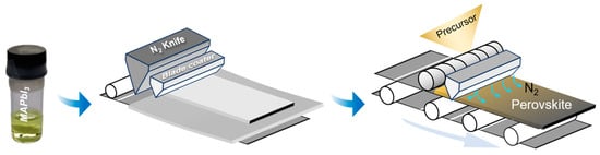
Figure 1.
Schematic of the doctor-blading procedure for perovskite film deposition.
2.4. Characterizations
The morphological and crystallographic properties of the films were observed using a scanning electron microscope (JSM-6307, JEOL Inc., Tokyo, Japan) and an X-ray diffractometer (SMART LAB, Rigaku, Tokyo, Japan), respectively. The UV–Vis transmission spectra of the films were measured with a JASCO V-570 UV/VIS/NIR Spectrometer. Using a fluorescence spectrometer (FLS980, Edinburgh Instruments, Livingston, UK), the photoluminescence (PL) and time-resolved photoluminescence (TRPL) spectra were acquired. To measure the J–V curves of the manufactured devices, a PV-IV-201V I-V Station (Newport Oriel, Irvine, CA, USA) was used. Previously, the source of illumination was rectified using a Newport 91150 V reference cell system. The J–V contours were scanned at 0.1 Vs−1, either from −0.1 V to 1.2 V or in the opposite direction. A Qtest Station 1000ADX (Growntech, Inc., Brentwood, Tennessee) was used to measure the external quantum efficiency (EQE) spectra of the devices. Electrochemical impedance spectroscopy (EIS) was performed using a Chenhua, Shanghai CHI660E electrochemical workstation.
3. Results and Discussion
Figure 2a demonstrates that the XRD patterns of the MAPbI3 films of varying thickness are identical, suggesting that N2 pressure does affect the structural properties of doctor-bladed perovskite films. All the samples show a pure phase of MAPbI3 with characteristic diffraction peaks at 14.2°, 28.5°, and 31.8°, which can be indexed to the (110), (220), and (222) planes of the MAPbI3, respectively. The mean crystal size was calculated using the Scherrer equation, which relates the FWHM of the XRD peaks to the crystal size. Using this equation, we calculated the high-intensity peak (110) for various N2 pressures of 0.2, 0.3, 0.4, 0.5, and 0.6 MPa and crystallite sizes of 694.41, 689.63, 656.69, 648.92, and 648.22 nm, respectively. The diffraction peak intensity decreases with the increase in N2 pressure, which should be ascribed to the decrease in film thickness, as demonstrated in Figure 2d. The optical absorption spectra in Figure 2c indicate that the MAPbI3 films have the same absorption onset. Nonetheless, the light absorption beyond the bandgap gradually decreases with reduced thickness. Figure 2d shows the MAPbI3 film thickness as a function of N2 flow pressure, indicating that the film thickness is inversely proportional to the N2 pressure. The corresponding cross-sectional SEM images are depicted in Figure 3.
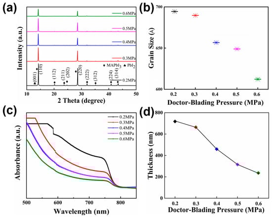
Figure 2.
(a) XRD patterns of MAPbI3 films. (b) Crystalline size of as-prepared MAPbI3 films fabricated with varying N2 input pressures during the doctor-blading process with the structure of ITO/Sn2O/MAPbI3. (c) Absorbance spectra of perovskite films deposited with different input N2 pressures on bare glass substrates. (d) The thickness of perovskite films as a function of the pressure of the input N2 gas.
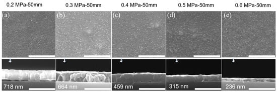
Figure 3.
Top-view and cross-sectional SEM images (a–e) of the MAPbI3 fabricated with varying N2 input pressures during the doctor-blading process. Scale bars 5 µm and 1 µm, respectively.
The top-view scanning electron microscopy (SEM) images in Figure 3a–e portray the morphology of perovskite films (on glass substrates) prepared via doctor blading, from which it can be observed that the grain size of the doctor-bladed films is larger than that of the conventional-method-produced film (which is consistent with the literature [43]). Increasing the N2 pressure during blade coating can result in more uniform film formation and enhanced surface coverage, which can facilitate the growth of larger grains and improve the overall crystallinity of the material. On the other hand, decreasing the N2 pressure can reduce the spread of the solution and result in a more porous and less compact, thicker film with a smaller grain size and reduced crystallinity. For the sake of simplicity, we solely examined the thickness control of 2 cm × 2 cm substrates. During the doctor-blading process, we regulated the pressure of the input N2 flow to customize the thickness of the MAPbI3 films. The thickness of the MAPbI3 film was inversely proportional to the N2 flow pressure. Figure 3a–e illustrates the SEM images of the respective top views and cross-sections. Since thickness can significantly affect film quality, perovskite films of varying thicknesses were evaluated to determine the ideal thickness for PV devices. The MAPbI3 films showed similar structural properties after tuning their thickness, while the optical and optoelectronic properties varied with different thicknesses.
Steady-state photoluminescence (PL) spectra were obtained to reveal the quality of the perovskite films deposited on quartz with varying input N2 pressure, with the subsequent outcomes shown in Figure 4a. The photoluminescence (PL) intensity of perovskite films can vary with the N2 pressure used during deposition, mainly when blade coating is employed. This is because the N2 pressure can impact the growth conditions and the film quality, affecting the PL performance. On the one hand, high N2 pressure can result in denser and more compact films, leading to a better PL performance. However, if the pressure is too high, it can also cause defects or inhomogeneities in the film, which can degrade the PL. On the other hand, low N2 pressure can lead to less compact and more porous films, resulting in reduced PL intensity. Therefore, identifying the optimal N2 pressure that balances the trade-off between film quality and PL performance can be challenging, and the ideal pressure can vary depending on the specific blade-coating conditions. In doctor blading, the most vigorous PL emission arises at a sample input N2 pressure of 0.5 MPa. Figure 4b shows the TRPL measurements, which provide additional evidence for the PL spectrum. The PL decay curves clearly exhibit biexponential decay behaviour, which can be modelled using the following biexponential equation [44]:
where A1 and A2 represent the decay amplitudes, τ1 and τ2 represent the carrier lifetime, and y0 represents an offset constant. The constants for trap-mediated nonradiative recombination and free carrier recombination from the bulk perovskite are the fast decay component τ1 and slow decay component τ2 [45,46]. The detailed results of the calibration are listed in Table 1. Using the equation below, the average carrier lifetime (τavg) can be calculated [47]:
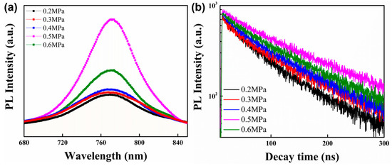
Figure 4.
(a) Steady-state PL and (b) TRPL spectra of perovskite films deposited via doctor blading on glass substrates with varying input N2 pressure.

Table 1.
A concise overview of the fitted parameters for the TRPL of perovskite films on bare glass substrates with varying N2 pressure inputs.
The average carrier lifetimes for the doctor-bladed films created with varying input N2 pressures (0.2, 0.3, 0.4, 0.5, and 0.6 MPa) are 91.54, 117.45, 120.21, 151.28, and 130.31 ns, respectively. The 0.5 MPa film’s carrier lifetime is longer than that of the other films, which can be attributed to its slower recombination rate and lower defect density than the other doctor-bladed films.
To fabricate fully printed perovskite solar cells, we tried to deposit SnO2 layers using the doctor-blading method and compared them with the spin-coated SnO2 layers. The top-view and cross-sectional SEM images in Figure S1 (see Supplementary Materials) illustrate the morphology of the SnO2 films (on the glass/ITO substrates) fabricated via spin-coating and doctor-blading procedures, respectively. It is clear that the doctor-bladed SnO2 film is thicker than the spin-coated SnO2 film. The transmission spectra in Figure S2 demonstrate that the spin-coated SnO2 film is comparable with the doctor-bladed SnO2 film. To investigate the effect of varying N2 pressure on cell performance, as shown in Figure 5a, we manufactured spin-coating-free PSCs with ITO/SnO2/perovskite utilizing methylamine-treated MAPbI3 as the light absorber. Figure 5b depicts a cross-sectional SEM image of a solar cell constructed with a MAPbI3 film at an N2 pressure input of 0.5 MPa. The overall device is highly consistent in appearance, and the ITO layer and perovskite film are around 190 and 315 nm thick, respectively. The SnO2 ETL is too thin to be discernible in the SEM image. Figure 5c demonstrates the J–V curves for the best-performing carbon devices with various perovskite films, whereas Table 2 summarises the full photovoltaic parameters. The device deposited with a 0.5 MPa N2 pressure yielded the highest PCE, with a PCE of 14.17%, Voc of 1.01 V, Jsc of 22.77 mA cm−2, and FF of 0.61.
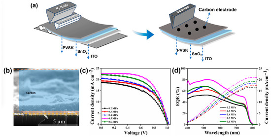
Figure 5.
(a) Diagrammatic structure of the manufactured device. (b) SEM image of the bilayer PSC in sections. (c) J–V curves for the best-performing devices. (d) EQE and integrated current density curves for the devices with perovskite layers with varied input N2 pressure. With an AM 1.5G illumination, the J–V curves were scanned in reverse directions.
Table 2.
Average photovoltaic parameters for the best-performing PSC devices manufactured with different N2 pressures.
Figure 5d conveys the external quantum efficiency (EQE) spectra for the devices, and the integral current densities for the fluctuating input N2 pressure (0.2, 0.3, 0.4, 0.5, and 0.6 MPa) devices are 16.65 mA cm−2, 17.33 mA cm−2, 18.44 mA cm−2, 20.97 mA cm−2, and 19.20 mA cm−2, respectively, which are comparable to those obtained from the J–V curves. We also attempted to create bigger devices, and Figure S3 depicts an example of a typical carbon-printed device pattern (over a square-inch substrate). This finding is consistent across multiple samples, indicating that the devices created with doctor blading are uniform. Figure S3 shows the related J–V curves and reliable PCE output; a stabilized output PCE 8.38% was attained. As demonstrated previously, the lower PCE with a greater cell size is primarily due to the reduced fill factor (FF) associated with higher series resistance.
We further performed electrochemical impedance measurements under light illumination to investigate the impact of varying input N2 pressure on the charge carrier behaviour of the devices under working conditions. Figure 6 shows the Nyquist plots with different N2 pressures under 1 sun illumination without bias at a minor voltage fluctuation (5 mV). By fitting the Nyquist plots to the equivalent circuit depicted in Figure 6, the charge transfer resistance of the devices at a given voltage could be determined. The curves are separated into two regions, with a high-frequency-area semicircle representing the charge transfer resistance (Rct) and a low-frequency-zone incomplete semicircle representing the recombination resistance (Rrec), and the resulting values are displayed in Table 3. These results verify an improved charge collection at a 0.5 MPa N2 pressure, consistent with the TRPL and stabilized output results. However, the 0.5 MPa sample, in the case of the N2 pressure input device, demonstrates the most substantial recombination resistance among all the samples, indicating efficient carrier extraction and less recombination [47], which enriches the device’s performance (FF) [44,47].
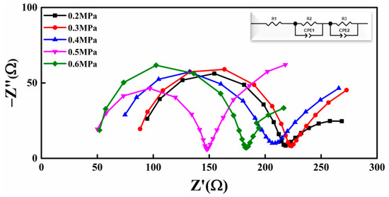
Figure 6.
The impedance spectra of PSCs of varying input N2 pressures under 1 sun illumination (AM 1.5 G, 100mW cm−2), with the insert depicting the equivalent circuit employed to fit the Nyquist plots.
Table 3.
Fitting parameters for EIS of PSC devices based on doctor blading with varying input N2 pressure.
All types of devices were constructed in many batches in order to further test for repeatability, and Figure 7a–d depicts the statistical results for the photovoltaic parameters. The device’s performance characteristics are constrained to an equitably slight range, and the device with an 0.5 MPa N2 pressure shows some variation among all the parameters.
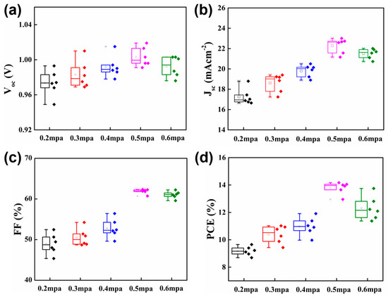
Figure 7.
Statistical photovoltaic parameters of (a) Voc, (b) Jsc, (c) FF, and (d) PCE were determined from different devices with perovskite layers and varying input N2 pressure in the reverse-scan mode with an AM 1.5G illumination.
4. Conclusions
In this study, we made a monumental breakthrough in the realm of doctor-blading techniques for the deposition of perovskite films and ETLs and the fabrication of entirely air-printed perovskite photovoltaic devices. We demonstrated a strategy for depositing MAPbI3 films in an ambient environment with doctor blading that is entirely free of spin coating and has precise morphological control. Consequently, fully printed perovskite solar cells with the structure of ITO/SnO2/MAPbI3/carbon were fabricated using a doctor-bladed SnO2 electron transport layer and a screen-printed carbon counter electrode. The device with an input N2 pressure of 0.5 MPa obtained a superior PCE of 14.17%, whereas the large-area device, with an active area of 1 cm2, yielded a stabilised PCE of 8.38%. This work addressed ambient-processed, fully spin-coating-free PSCs with the merits of industrialization, scalability, and stability. This research could have significant implications for the development of efficient and cost-effective perovskite solar cells.
Supplementary Materials
The following supporting information can be downloaded at: https://www.mdpi.com/article/10.3390/coatings13081338/s1, Figure S1: The top-view and cross-sectional SEM images of SnO2 films deposited using the spin-coating process and the doctor-blading process; Figure S2: Transmission spectra of SnO2 films deposited via spin-coating and doctor-blading processes on glass substrates; Figure S3: Doctor-bladed MAPbI3 film J–V characteristics of the best-performing device with an illumination exposure area of 1.0 cm2, Table S1: A summary of all the highest-performing carbon-based HTL-free PSCs reported thus far. The top-view and cross-sectional SEM images of SnO2 films deposited using spin-coating and doctor-blading process, transmission spectra of SnO2 films deposited using doctor-blading and spin-coating processes on the glass/ITO substrates, and doctor-bladed MAPbI3 film J–V characteristics of the best-performing device with an illumination-exposure area of 1.0 cm2. References [48,49,50,51,52,53,54,55,56,57,58,59,60,61,62,63,64,65,66,67,68,69,70,71,72] are cited in the supplementary materials.
Author Contributions
Writing—original draft, S.I.; Writing—review and editing, B.W., J.Z. (Jiawei Zhang), M.Z.N. and J.Z. (Jide Zhang); Supervision, X.Y. and W.Q. All authors have read and agreed to the published version of the manuscript.
Funding
This work was funded by the Fundamental Research Funds for the Central Universities (xzy 012022090).
Institutional Review Board Statement
Not applicable.
Informed Consent Statement
Not applicable.
Data Availability Statement
Data sharing is not applicable to this article.
Acknowledgments
The SEM work was conducted at the International Center for Dielectric Research. The authors sincerely thank Hang Guo of the Instrument Analysis Center of Xi’an Jiaotong University for her assistance with the PL and TRPL analyses.
Conflicts of Interest
The authors declare no conflict of interest.
References
- NREL. NREL Efficiency Chart. Available online: https://www.nrel.gov/pv/assets/pdfs/best-research-cell-efficiencies.pdf (accessed on 3 March 2023).
- Xu, L.; Chon, M.J.; Mills, B.; Thompson, C.V. Mechanical stress and morphology evolution in RuO2 thin film electrodes during lithiation and delithiation. J. Power Sources 2022, 552, 232260. [Google Scholar] [CrossRef]
- Xu, L.; Thompson, C.V. Mechanisms of the cyclic (de) lithiation of RuO2. J. Mater. Chem. A 2020, 8, 21872–21881. [Google Scholar] [CrossRef]
- Zhao, Y.; Zhu, K. Organic–inorganic hybrid lead halide perovskites for optoelectronic and electronic applications. Chem. Soc. Rev. 2016, 45, 655–689. [Google Scholar] [CrossRef] [PubMed]
- Zhang, W.; Eperon, G.E.; Snaith, H.J. Metal halide perovskites for energy applications. Nat. Energy 2016, 1, 16048. [Google Scholar] [CrossRef]
- Hajjiah, A.; Gamal, M.; Kandas, I.; Gorji, N.E.; Shehata, N. DFT and AMPS-1D simulation analysis of all-perovskite solar cells based on CsPbI3/FAPbI3 bilayer structure. Sol. Energy Mater. Sol. Cells 2022, 248, 112026. [Google Scholar] [CrossRef]
- Li, X.; Bi, D.; Yi, C.; Décoppet, J.-D.; Luo, J.; Zakeeruddin, S.M.; Hagfeldt, A.; Grätzel, M. A vacuum flash–assisted solution process for high-efficiency large-area perovskite solar cells. Science 2016, 353, 58–62. [Google Scholar] [CrossRef]
- Ding, B.; Li, Y.; Huang, S.-Y.; Chu, Q.-Q.; Li, C.-X.; Li, C.-J.; Yang, G.-J. Material nucleation/growth competition tuning towards highly reproducible planar perovskite solar cells with efficiency exceeding 20%. J. Mater. Chem. A 2017, 5, 6840–6848. [Google Scholar] [CrossRef]
- Han, Q.; Ding, J.; Bai, Y.; Li, T.; Ma, J.-Y.; Chen, Y.-X.; Zhou, Y.; Liu, J.; Ge, Q.-Q.; Chen, J. Carrier dynamics engineering for high-performance electron-transport-layer-free perovskite photovoltaics. Chem 2018, 4, 2405–2417. [Google Scholar] [CrossRef]
- Wu, Y.; Xie, F.; Chen, H.; Yang, X.; Su, H.; Cai, M.; Zhou, Z.; Noda, T.; Han, L. Thermally stable MAPbI3 perovskite solar cells with efficiency of 19.19% and area over 1 cm2 achieved by additive engineering. Adv. Mater. 2017, 29, 1701073. [Google Scholar] [CrossRef]
- Yang, M.; Zhou, Y.; Zeng, Y.; Jiang, C.S.; Padture, N.P.; Zhu, K. Square-centimeter solution-processed planar CH3NH3PbI3 perovskite solar cells with efficiency exceeding 15%. Adv. Mater. 2015, 27, 6363–6370. [Google Scholar] [CrossRef]
- Xiao, M.; Huang, F.; Huang, W.; Dkhissi, Y.; Zhu, Y.; Etheridge, J.; Gray-Weale, A.; Bach, U.; Cheng, Y.B.; Spiccia, L. A fast deposition-crystallization procedure for highly efficient lead iodide perovskite thin-film solar cells. Angew. Chem. Int. Ed. 2014, 53, 9898–9903. [Google Scholar] [CrossRef] [PubMed]
- Chen, H.; Ye, F.; Tang, W.; He, J.; Yin, M.; Wang, Y.; Xie, F.; Bi, E.; Yang, X.; Grätzel, M. A solvent-and vacuum-free route to large-area perovskite films for efficient solar modules. Nature 2017, 550, 92–95. [Google Scholar] [CrossRef]
- Ye, F.; Chen, H.; Xie, F.; Tang, W.; Yin, M.; He, J.; Bi, E.; Wang, Y.; Yang, X.; Han, L. Soft-cover deposition of scaling-up uniform perovskite thin films for high cost-performance solar cells. Energy Environ. Sci. 2016, 9, 2295–2301. [Google Scholar] [CrossRef]
- Padhiar, M.A.; Wang, M.; Ji, Y.; Yang, Z.; Zhou, Y.; Qiu, H.; Wang, H.; Shah, A.A.; Bhatti, A.S. Stable CsPbX3 (Br/Cl) Perovskite Nanocrystal Layer Passivated with Al-Doped CdSe for Blue Light-Emitting Diodes. ACS Appl. Nano Mater. 2021, 5, 908–916. [Google Scholar] [CrossRef]
- Xu, L.; Meng, T.; Zheng, X.; Li, T.; Brozena, A.H.; Mao, Y.; Zhang, Q.; Clifford, B.C.; Rao, J.; Hu, L. Nanocellulose-Carboxymethylcellulose Electrolyte for Stable, High-Rate Zinc-Ion Batteries. Adv. Funct. Mater. 2023, 33, 2302098. [Google Scholar] [CrossRef]
- Wu, M.; Zhang, Y.; Xu, L.; Yang, C.; Hong, M.; Cui, M.; Clifford, B.C.; He, S.; Jing, S.; Yao, Y. A sustainable chitosan-zinc electrolyte for high-rate zinc-metal batteries. Matter 2022, 5, 3402–3416. [Google Scholar] [CrossRef]
- Huang, H.; Shi, J.; Zhu, L.; Li, D.; Luo, Y.; Meng, Q. Two-step ultrasonic spray deposition of CH3NH3PbI3 for efficient and large-area perovskite solar cell. Nano Energy 2016, 27, 352–358. [Google Scholar] [CrossRef]
- Barrows, A.T.; Pearson, A.J.; Kwak, C.K.; Dunbar, A.D.; Buckley, A.R.; Lidzey, D.G. Efficient planar heterojunction mixed-halide perovskite solar cells deposited via spray-deposition. Energy Environ. Sci. 2014, 7, 2944–2950. [Google Scholar] [CrossRef]
- Zuo, C.; Vak, D.; Angmo, D.; Ding, L.; Gao, M. One-step roll-to-roll air processed high efficiency perovskite solar cells. Nano Energy 2018, 46, 185–192. [Google Scholar] [CrossRef]
- Wei, Z.; Chen, H.; Yan, K.; Yang, S. Inkjet printing and instant chemical transformation of a CH3NH3PbI3/nanocarbon electrode and interface for planar perovskite solar cells. Angew. Chem. Int. Ed. 2014, 53, 13239–13243. [Google Scholar] [CrossRef]
- Mei, A.; Li, X.; Liu, L.; Ku, Z.; Liu, T.; Rong, Y.; Xu, M.; Hu, M.; Chen, J.; Yang, Y. A hole-conductor–free, fully printable mesoscopic perovskite solar cell with high stability. Science 2014, 345, 295–298. [Google Scholar] [CrossRef] [PubMed]
- Lee, J.-W.; Na, S.-I.; Kim, S.-S. Efficient spin-coating-free planar heterojunction perovskite solar cells fabricated with successive brush-painting. J. Power Sources 2017, 339, 33–40. [Google Scholar] [CrossRef]
- Koza, J.A.; Hill, J.C.; Demster, A.C.; Switzer, J.A. Epitaxial electrodeposition of methylammonium lead iodide perovskites. Chem. Mater. 2016, 28, 399–405. [Google Scholar] [CrossRef]
- Deng, Y.; Peng, E.; Shao, Y.; Xiao, Z.; Dong, Q.; Huang, J. Scalable fabrication of efficient organolead trihalide perovskite solar cells with doctor-bladed active layers. Energy Environ. Sci. 2015, 8, 1544–1550. [Google Scholar] [CrossRef]
- Di Giacomo, F.; Shanmugam, S.; Fledderus, H.; Bruijnaers, B.J.; Verhees, W.J.; Dorenkamper, M.S.; Veenstra, S.C.; Qiu, W.; Gehlhaar, R.; Merckx, T. Up-scalable sheet-to-sheet production of high efficiency perovskite module and solar cells on 6-in. substrate using slot die coating. Sol. Energy Mater. Sol. Cells 2018, 181, 53–59. [Google Scholar] [CrossRef]
- Vak, D.; Hwang, K.; Faulks, A.; Jung, Y.S.; Clark, N.; Kim, D.Y.; Wilson, G.J.; Watkins, S.E. 3D printer based slot-die coater as a lab-to-fab translation tool for solution-processed solar cells. Adv. Energy Mater. 2015, 5, 1401539. [Google Scholar] [CrossRef]
- Ye, F.; Tang, W.; Xie, F.; Yin, M.; He, J.; Wang, Y.; Chen, H.; Qiang, Y.; Yang, X.; Han, L. Low-Temperature Soft-Cover Deposition of Uniform Large-Scale Perovskite Films for High-Performance Solar Cells. Adv. Mater. 2017, 29, 1701440. [Google Scholar] [CrossRef] [PubMed]
- Luo, J.; Xia, J.; Yang, H.; Sun, C.; Li, N.; Malik, H.A.; Shu, H.; Wan, Z.; Zhang, H.; Brabec, C.J. A pressure process for efficient and stable perovskite solar cells. Nano Energy 2020, 77, 105063. [Google Scholar] [CrossRef]
- Schackmar, F.; Eggers, H.; Frericks, M.; Richards, B.S.; Lemmer, U.; Hernandez-Sosa, G.; Paetzold, U.W. Perovskite solar cells with all-inkjet-printed absorber and charge transport layers. Adv. Mater. Technol. 2021, 6, 2000271. [Google Scholar] [CrossRef]
- Li, S.; Xie, H.; Dong, Q.; Jing, S.; Li, T.; Xu, L.; Hu, L. Synthesizing Carbon-Supported, High-Loading, Ultra-Small Pt3Ni Nanoparticles via Tuning the Surface Electrostatic Effect. Small Struct. 2023, 4, 2200176. [Google Scholar] [CrossRef]
- Song, S.; Hörantner, M.T.; Choi, K.; Snaith, H.J.; Park, T. Inducing swift nucleation morphology control for efficient planar perovskite solar cells by hot-air quenching. J. Mater. Chem. A 2017, 5, 3812–3818. [Google Scholar] [CrossRef]
- Chalkias, D.A.; Mourtzikou, A.; Katsagounos, G.; Karavioti, A.; Kalarakis, A.N.; Stathatos, E. Suppression of Coffee-Ring Effect in Air-Processed Inkjet-Printed Perovskite Layer toward the Fabrication of Efficient Large-Sized All-Printed Photovoltaics: A Perovskite Precursor Ink Concentration Regulation Strategy. Sol. RRL 2022, 6, 2200196. [Google Scholar] [CrossRef]
- He, M.; Li, B.; Cui, X.; Jiang, B.; He, Y.; Chen, Y.; O’Neil, D.; Szymanski, P.; Ei-Sayed, M.A.; Huang, J. Meniscus-assisted solution printing of large-grained perovskite films for high-efficiency solar cells. Nat. Commun. 2017, 8, 16045. [Google Scholar] [CrossRef] [PubMed]
- Zhang, C.; Yin, X.; Chen, G.; Sang, Z.; Yang, Y.; Que, W. High-Performance Photodetector with a-IGZO/PbS Quantum Dots Heterojunction. ACS Photonics 2023, 10, 790–800. [Google Scholar] [CrossRef]
- Zhang, Y.; Cui, Q.-p.; Shao, F.-q.; Wang, J.-s.; Zhao, H.-y. Influence of air-knife wiping on coating thickness in hot-dip galvanizing. J. Iron Steel Res. Int. 2012, 19, 70–78. [Google Scholar] [CrossRef]
- Cho, T.-S.; Kwon, Y.-D.; Kwon, S.-B. A study of the influence of air-knife tilting on coating thickness in hot-dip galvanizing. J. Therm. Sci. 2009, 18, 262–267. [Google Scholar] [CrossRef]
- Ghosh, A.K.; Jeong, B.-H.; Huang, X.; Hoek, E.M. Impacts of reaction and curing conditions on polyamide composite reverse osmosis membrane properties. J. Membr. Sci. 2008, 311, 34–45. [Google Scholar] [CrossRef]
- Kwon, S.-B.; Lee, D.-W.; Kwon, Y.-D. Experimental and computational studies on Coanda nozzle flow for the air knife application. J. Therm. Sci. 2007, 16, 164–169. [Google Scholar] [CrossRef]
- Zhou, Y.; Zhao, Y. Chemical stability and instability of inorganic halide perovskites. Energy Environ. Sci. 2019, 12, 1495–1511. [Google Scholar] [CrossRef]
- Maity, K.; Pal, U.; Mishra, H.K.; Maji, P.; Sadhukhan, P.; Mallick, Z.; Das, S.; Mondal, B.; Mandal, D. Piezo-phototronic effect in highly stable CsPbI3-PVDF composite for self-powered nanogenerator and photodetector. Nano Energy 2022, 92, 106743. [Google Scholar] [CrossRef]
- Iqbal, S.; Xie, H.; Yin, X.; Guo, Y.; Zhang, C.; Liu, D.; Wang, B.; Gao, B.; Que, W. Methylamine-Based Method to Deposit MAPbI3 Nanoscale-Thick Films for Efficient Perovskite Solar Cells with Carbon Electrodes. ACS Appl. Nano Mater. 2022, 5, 4112–4118. [Google Scholar] [CrossRef]
- Jeon, N.J.; Noh, J.H.; Kim, Y.C.; Yang, W.S.; Ryu, S.; Seok, S.I. Solvent engineering for high-performance inorganic–organic hybrid perovskite solar cells. Nat. Mater. 2014, 13, 897–903. [Google Scholar] [CrossRef] [PubMed]
- Zhang, Z.; Men, B.; Liu, Y.; Gao, H.; Mao, Y. Effects of precursor solution composition on the performance and IV hysteresis of perovskite solar cells based on CH3NH3PbI3-xClx. Nanoscale Res. Lett. 2017, 12, 84. [Google Scholar] [CrossRef]
- Liu, G.; Zheng, H.; Xu, X.; Zhu, L.; Alsaedi, A.; Hayat, T.; Pan, X.; Dai, S. Efficient solar cells with enhanced humidity and heat stability based on benzylammonium–caesium–formamidinium mixed-dimensional perovskites. J. Mater. Chem. A 2018, 6, 18067–18074. [Google Scholar] [CrossRef]
- Yang, D.; Yang, R.; Ren, X.; Zhu, X.; Yang, Z.; Li, C.; Liu, S. Hysteresis-suppressed high-efficiency flexible perovskite solar cells using solid-state ionic-liquids for effective electron transport. Adv. Mater. 2016, 28, 5206–5213. [Google Scholar] [CrossRef]
- Miao, Y.; Chen, Y.; Chen, H.; Wang, X.; Zhao, Y. Using steric hindrance to manipulate and stabilize metal halide perovskites for optoelectronics. Chem. Sci. 2021, 12, 7231–7247. [Google Scholar] [CrossRef]
- Zhou, H.; Shi, Y.; Wang, K.; Dong, Q.; Bai, X.; Xing, Y.; Du, Y.; Ma, T. Low-Temperature Processed and Carbon-Based Zno/Ch3nh3pbi3/C Planar Heterojunction Perovskite Solar Cells. J. Phys. Chem. C 2015, 119, 4600–4605. [Google Scholar] [CrossRef]
- Cheng, N.; Liu, P.; Qi, F.; Xiao, Y.; Yu, W.; Yu, Z.; Liu, W.; Guo, S.-S.; Zhao, X.-Z. Multi-walled carbon nanotubes act as charge transport channel to boost the efficiency of hole transport material free perovskite solar cells. J. Power Sources 2016, 332, 24–29. [Google Scholar] [CrossRef]
- Nouri, E.; Mohammadi, M.R.; Lianos, P. Inverted perovskite solar cells based on lithium-functionalized graphene oxide as an electron-transporting layer. Chem. Commun. 2017, 53, 1630–1633. [Google Scholar] [CrossRef]
- Xu, X.; Zhang, H.; Cao, K.; Cui, J.; Lu, J.; Zeng, X.; Shen, Y.; Wang, M. Lead Methylammonium Triiodide Perovskite-Based Solar Cells: An Interfacial Charge-Transfer Investigation. Chemsuschem 2014, 7, 3088–3094. [Google Scholar] [CrossRef]
- Li, J.; Yao, J.X.; Liao, X.Y.; Yu, R.L.; Xia, H.R.; Sun, W.T.; Peng, L.M. A contact study in hole conductor free perovskite solar cells with low temperature processed carbon electrodes. RSC Adv. 2017, 7, 20732–20737. [Google Scholar] [CrossRef]
- Xiao, Y.; Cheng, N.; Kondamareddy, K.K.; Wang, C.; Liu, P.; Guo, S.; Zhao, X.Z. W-doped TiO2 mesoporous electron transport layer for efficient hole transport material free perovskite solar cells employing carbon counter electrodes. J. Power Sources 2017, 342, 489–494. [Google Scholar] [CrossRef]
- Chen, M.; Zha, R.H.; Yuan, Z.Y.; Jing, Q.S.; Huang, Z.Y.; Yang, X.K.; Yang, S.M.; Zhao, X.H.; Xu, D.L.; Zou, G.D. Boron and phosphorus co-doped carbon counter electrode for efficient hole-conductor-free perovskite solar cell. Chem. Eng. J. 2017, 313, 791–800. [Google Scholar] [CrossRef]
- Zhang, C.; Luo, Y.; Chen, X.; Chen, Y.; Sun, Z.; Huang, S. Effective improvement of the photovoltaic performance of carbon-based perovskite solar cells by additional solvents. Nanomicro. Lett. 2016, 8, 347–357. [Google Scholar]
- Duan, M.; Hu, Y.; Mei, A.; Rong, Y.; Han, H. Printable carbon-based hole-conductor-free mesoscopic perovskite solar cells: From lab to market. Mater. Today Energy 2018, 7, 221–231. [Google Scholar] [CrossRef]
- Chen, J.; Xiong, Y.; Rong, Y.; Mei, A.; Sheng, Y.; Jiang, P.; Hu, Y.; Li, X.; Han, H. Solvent effect on the hole-conductor-free fully printable perovskite solar cells. Nano Energy 2016, 27, 130–137. [Google Scholar] [CrossRef]
- Rong, Y.; Hou, X.; Hu, Y.; Mei, A.; Liu, L.; Wang, P.; Han, H. Synergy of ammonium chloride and moisture on perovskite crystallization for efficient printable mesoscopic solar cells. Nat. Commun. 2017, 8, 14555. [Google Scholar] [CrossRef]
- Liu, Z.; Zhang, M.; Xu, X.; Bu, L.; Zhang, W.; Li, W.; Zhao, Z.; Wang, M.; Cheng, Y.-B.; He, H. p-Type mesoscopic NiO as an active interfacial layer for carbon counter electrode based perovskite solar cells. Dalton Trans. 2014, 44, 3967–3973. [Google Scholar] [CrossRef]
- Liu, H.; Dong, M.; Huang, W.; Gao, J.; Dai, K.; Guo, J.; Zheng, G.; Liu, C.; Shen, C.; Guo, Z. Lightweight conductive graphene/thermoplastic polyurethane foams with ultrahigh compressibility for piezoresistive sensing. J. Mater. Chem. C 2016, 5, 73–83. [Google Scholar] [CrossRef]
- Chang, X.; Li, W.; Chen, H.; Zhu, L.; Liu, H.; Geng, H.; Xiang, S.; Liu, J.; Zheng, X.; Yang, Y.; et al. Colloidal precursor-induced growth of ultra-even CH3NH3PbI3 for high-performance paintable carbon-based perovskite solar cells. ACS Appl. Mater. Interfaces 2016, 8, 30184–30192. [Google Scholar] [CrossRef]
- Tsai, C.-M.; Wu, G.-W.; Narra, S.; Chang, H.-M.; Mohanta, N.; Wu, H.-P.; Wang, C.-L.; Diau, E.W.-G. Control of preferred orientation with slow crystallization for carbon-based mesoscopic perovskite solar cells attaining efficiency 15%. J. Mater. Chem. A 2016, 5, 739–747. [Google Scholar] [CrossRef]
- Chen, H.; Wei, Z.; He, H.; Zheng, X.; Wong, K.S.; Yang, S. Solvent engineering boosts the efficiency of paintable carbon-based perovskite solar cells to beyond 14%. Adv. Energy Mater. 2016, 6, 1502087. [Google Scholar] [CrossRef]
- Chen, H.; Zheng, X.; Li, Q.; Yang, Y.; Xiao, S.; Hu, C.; Bai, Y.; Zhang, T.; Wong, K.S.; Yang, S. An amorphous precursor route to the conformable oriented crystallization of CH3NH3PbBr3in mesoporous scaffolds: Toward efficient and thermally stable carbon-based perovskite solar cells. J. Mater. Chem. A 2016, 4, 12897–12912. [Google Scholar] [CrossRef]
- Yue, G.; Chen, D.; Wang, P.; Zhang, J.; Hu, Z.; Zhu, Y. Low-temperature prepared carbon electrodes for hole-conductor-free mesoscopic perovskite solar cells. Electrochim. Acta 2016, 218, 84–90. [Google Scholar] [CrossRef]
- Zheng, X.; Chen, H.; Li, Q.; Yang, Y.; Wei, Z.; Bai, Y.; Qiu, Y.; Zhou, D.; Wong, K.S.; Yang, S. Boron Doping of Multiwalled Carbon Nanotubes Significantly Enhances Hole Extraction in Carbon-Based Perovskite Solar Cells. Nano Lett. 2017, 17, 2496–2505. [Google Scholar] [CrossRef] [PubMed]
- Wei, Z.; Chen, H.; Yan, K.; Zheng, X.; Yang, S. Hysteresis-free multi-walled carbon nanotube-based perovskite solar cells with a high fill factor. J. Mater. Chem. A 2015, 3, 24226–24231. [Google Scholar] [CrossRef]
- Feng, J.; Wang, W.J.; Hai, X.; Yu, Y.L.; Wang, J.H. Green preparation of nitrogen-doped carbon dots derived from silkworm chrysalis for cell imaging. J. Mater. Chem. B 2016, 4, 387–393. [Google Scholar] [CrossRef]
- Jena, A.K.; Miyasaka, T. Hysteresis Characteristics and Device Stability. In Organic-Inorganic Halide Perovskite Photovoltaics; Park, N.G., Grätzel, M., Miyasaka, T., Eds.; Springer: Cham, Switzerland, 2016. [Google Scholar] [CrossRef]
- Chen, J.; Rong, Y.; Mei, A.; Xiong, Y.; Liu, T.; Sheng, Y.; Jiang, P.; Hong, L.; Guan, Y.; Zhu, X.; et al. Hole-conductor-free fully printable mesoscopic solar cell with mixed-anion perovskite CH3NH3PbI (3−x)(BF4) x. Adv. Energy Mater. 2016, 6, 1502009. [Google Scholar] [CrossRef]
- Cao, K.; Cui, J.; Zhang, H.; Li, H.; Song, J.; Shen, Y.; Cheng, Y.; Wang, M. Efficient mesoscopic perovskite solar cells based on the CH 3 NH 3 PbI 2 Br light absorber. J. Mater. Chem. A 2015, 3, 9116–9122. [Google Scholar] [CrossRef]
- Liu, Z.; Shi, T.; Tang, Z.; Sun, B.; Liao, G. Using a low-temperature carbon electrode for preparing hole-conductor-free perovskite heterojunction solar cells under high relative humidity. Nanoscale 2016, 8, 7017–7023. [Google Scholar] [CrossRef]
Disclaimer/Publisher’s Note: The statements, opinions and data contained in all publications are solely those of the individual author(s) and contributor(s) and not of MDPI and/or the editor(s). MDPI and/or the editor(s) disclaim responsibility for any injury to people or property resulting from any ideas, methods, instructions or products referred to in the content. |
© 2023 by the authors. Licensee MDPI, Basel, Switzerland. This article is an open access article distributed under the terms and conditions of the Creative Commons Attribution (CC BY) license (https://creativecommons.org/licenses/by/4.0/).