Article

Optical Characterization of Al Island Films: A Round Robin Test

by
Jordi Sancho-Parramon
1,*,
Tatiana Amochkina
2,†,
Steffen Wilbrandt
3,†,
Hrishikesh Kamble
1,
Vesna Janicki
1,
Krešimir Salamon
1,
Olaf Stenzel
3 and
Michael Trubetskov
2,4
1
Ruđer Bošković Institute, Bijenička Cesta 54, 10000 Zagreb, Croatia
2
OTF Studio GmbH, Watzmannring 71, 85748 Garching, Germany
3
Fraunhofer Institute for Applied Optics and Precision Engineering, Albert-Einstein-Str. 7, 07745 Jena, Germany
4
Max-Planck Institute of Quantum Optics, Hans-Kopfermann Str. 1, 85748 Garching, Germany
*
Author to whom correspondence should be addressed.
These authors contributed equally to this work.
Coatings 2023, 13(6), 1073; https://doi.org/10.3390/coatings13061073
Submission received: 5 May 2023 / Revised: 2 June 2023 / Accepted: 4 June 2023 / Published: 9 June 2023

Abstract

:
The determination of the effective optical constants of metal island films is an essential step towards the practical incorporation of this kind of films in optical coatings. In this work, the optical properties of aluminium island films deposited by electron beam evaporation on quartz substrates are investigated using different approaches employed by three research groups. The effective optical constants of the island films are inferred from optical measurements (spectrophotometry and spectroscopic ellipsometry) using: (i) a parameter-free dispersion model, (ii) a multiple oscillator model based on Gaussian line-shapes and (iii) the  β  distributed oscillator model. All the used approaches provide similar physical insights, i.e., an increase in the effective thickness of the metal island film, a red-shift and broadening of the plasmon resonance and an enhancement of the infrared absorption as the amount of deposited material increases. However, the optimal values of the effective optical constants and thickness significantly depend on the employed model and the experimental data used for data fitting.

1. Introduction

Metals islands films (MIFs) are nearly two-dimensional random or regular arrangements of nano-clusters that may be obtained during the first stages of metal deposition on dielectric surfaces [1]. They exhibit a highly tunable optical behaviour due to isolated nanoparticles’ localized surface plasmon resonance, which is strongly dependent on particle morphology and interparticle distance. A Drude-like response can also be observed if a conductive network of clusters is formed [2]. As a result, MIFs are used in a wide variety of photonic applications, including lithography-free metasurfaces [3], colour coatings [4,5] and selective absorbers [6,7].
In order to incorporate MIFs as building blocks in the design of optical coatings, a precise knowledge of their optical properties is needed [8]. The most common approach consists of modelling MIFs as homogeneous films with effective thicknesses and effective optical constants inferred from optical measurements. However, in contrast to standard metals or dielectrics used in optical coatings technology, the optimal dispersion model that can represent the effective optical constants of MIFs over a wide spectral range is not well settled. Classical effective medium theories, such as the Bruggeman or Maxwell-Garnett models, provide only a rough approximation [9] and have to be extended by explicitly incorporating a distribution of depolarization factors that arises from the particle size and shape distribution [10,11]. Alternatively, multiple-oscillator approaches [12,13] or non-parametric models with regularized smooth dispersion [14] have been successfully used to describe the optical response of MIFs. It has been shown that the classical Lorentz oscillator inaccurately describes the optical constants of such films, for it has wide absorption tails that are not observed experimentally. Instead, the Gaussian oscillator provides an absorption line shape more confined around the resonance frequency and better describes experimental data [15,16]. The Gaussian oscillator can be understood as a limiting case of a broad Gaussian distribution of Lorentzian resonances [17]. The absorption line-shape of island films often displays inhomogeneous line broadening that mathematically requires the use of two or more symmetric oscillators per resonance [9]. In this context, a  β -distribution of Lorentzian resonances inherently provides such inhomogeneous line broadening [18] along with a clear physical interpretation of the model parameters [19] and has been validated in the case of island films [20] and compact thin metal films [21]. On the other hand, non-parametric models make no a priori assumption on the optical constants dispersion and therefore are more flexible than models based on dispersion equations [14,22]. Nevertheless, non-parametric modelling treats real and imaginary parts of the optical constants as independent quantities and it is usually required to use penalty or regularization functions to avoid non-physical solutions [23].
In the present work, we investigate different approaches employed by three research groups for the optical characterization of MIFs using spectrophotometry and spectroscopic ellipsometry. In particular, we compare the results obtained using: (i) a non-parametric model [22,24], (ii) a multiple oscillator approach based on Gaussian line-shapes [15] and (iii) the  β -distributed oscillator model [18]. Aluminium island films were chosen for this round-robin test since they have a strong potential for the practical implementation of plasmonic-based structural colours [25]. In addition, interband transitions in the near-infrared range that overlaps with the free-electron response, possible Al oxidation during deposition even in near ultra high vacuum conditions [26], and the presence of a thin Al 2 O 3  layer covering the Al islands make the characterization of Al MIFs particularly challenging [27,28].

2. Materials and Methods

2.1. Fabrication and Measurements

Al island films were deposited on 1 mm thick quartz substrates by electron beam evaporation in a modified Varian chamber. In order to enhance island formation, the substrates were pre-heated at 220 °C before Al deposition and the deposition rate was ≈0.5 Å/s. Film mass thickness was controlled by quartz crystal monitoring and the deposition rate was adjusted by regulating the electron beam power. The base pressure was kept to 10 6  torr. Al islands films with mass thicknesses ( d A l ) of 3, 10, 12, 15, 24 and 32 nm were obtained. Under these deposition conditions, partial Al oxidation might take place [26]. In order to avoid further Al oxidation upon exposure to the atmosphere, the islands were coated with a thin Al 2 O 3  film (10 nm mass thickness). Al island films were deposited from the evaporation of Al wires while Al 2 O 3  films were deposited from Al 2 O 3  pellets. Characterization of single Al 2 O 3  film confirmed that the films were stoichiometric.
Transmission (normal incidence) and reflectance (6° incidence) spectra were taken in the range 250–1100 nm using 1 nm intervals with a UV/Vis Lambda 25 Perkin Elmer spectrophotometer. A Perkin Elmer Standard calibrated mirror (PE1000192) was used as a reference for reflectance measurements. Ellipsometric angles ( Δ , Ψ ) and degrees of depolarization (percentage of light that becomes unpolarized upon reflection) were obtained with a J. A. Woollam V-VASE ellipsometer in the spectral range between 0.57–5 eV (approximately 250–2175 nm) at 0.02 eV steps. Ellipsometric measurements were performed at angles of incidence of 45°, 55° and 65°. Depolarization essentially appears as a result of light reflected from the substrate backside, that reaches the detector and is added incoherently to the light reflected from the film side.
Scanning electron microscopy (SEM) measurements were done to connect the insights obtained by optical measurements with the sample morphology. In order to avoid sample charging issues, measurements were performed on Al islands deposited on Si wafers coated with a SiO 2  layer. To better observe islands morphology, these samples were not coated with the Al 2 O 3  overlayer. Plain view images were taken using a field-emission microscope Jeol JSM 7000F at an acceleration voltage of 1 kV. Surface elemental analysis was done by energy dispersive spectroscopy (EDS) with an EDS/INCA 350 (energy dispersive X-ray analyzer) unit linked to the microscope. X-ray diffraction (XRD) measurements were performed on selected samples to verify the island composition and to check for possible contamination/oxidation issues.

2.2. Optical Characterization Approaches

We used three different methods based on the inverse synthesis approach [29] that are usually employed by the groups involved in the joint study. In all cases, the samples were modelled as three-layer systems: glass substrate, Al island film and Al 2 O 3  overlayer. It was observed that more elementary modelling, such as considering the Al film and the Al 2 O 3  as a single homogeneous medium, was unable to provide good data fits for most of the samples.
The optical constants of the glass substrate and the Al 2 O 3  overlayer were fixed to literature values [30] and to results obtained from single layer characterization, respectively. The effective thickness of the Al island film ( d M I F ) and the Al 2 O 3  overlayer ( d A l 2 O 3 ) were allowed to differ from the deposited mass thickness to account for the island geometry of the film and the possible partial Al oxidation during the deposition process. The main differences among the approaches were (i) the modelling of the MIF effective optical constants dispersion and (ii) the definition of the discrepancy function that quantifies the difference between experimental and computed data and that can account for several types of experimental data and possible parameter regularization during the optimization process.
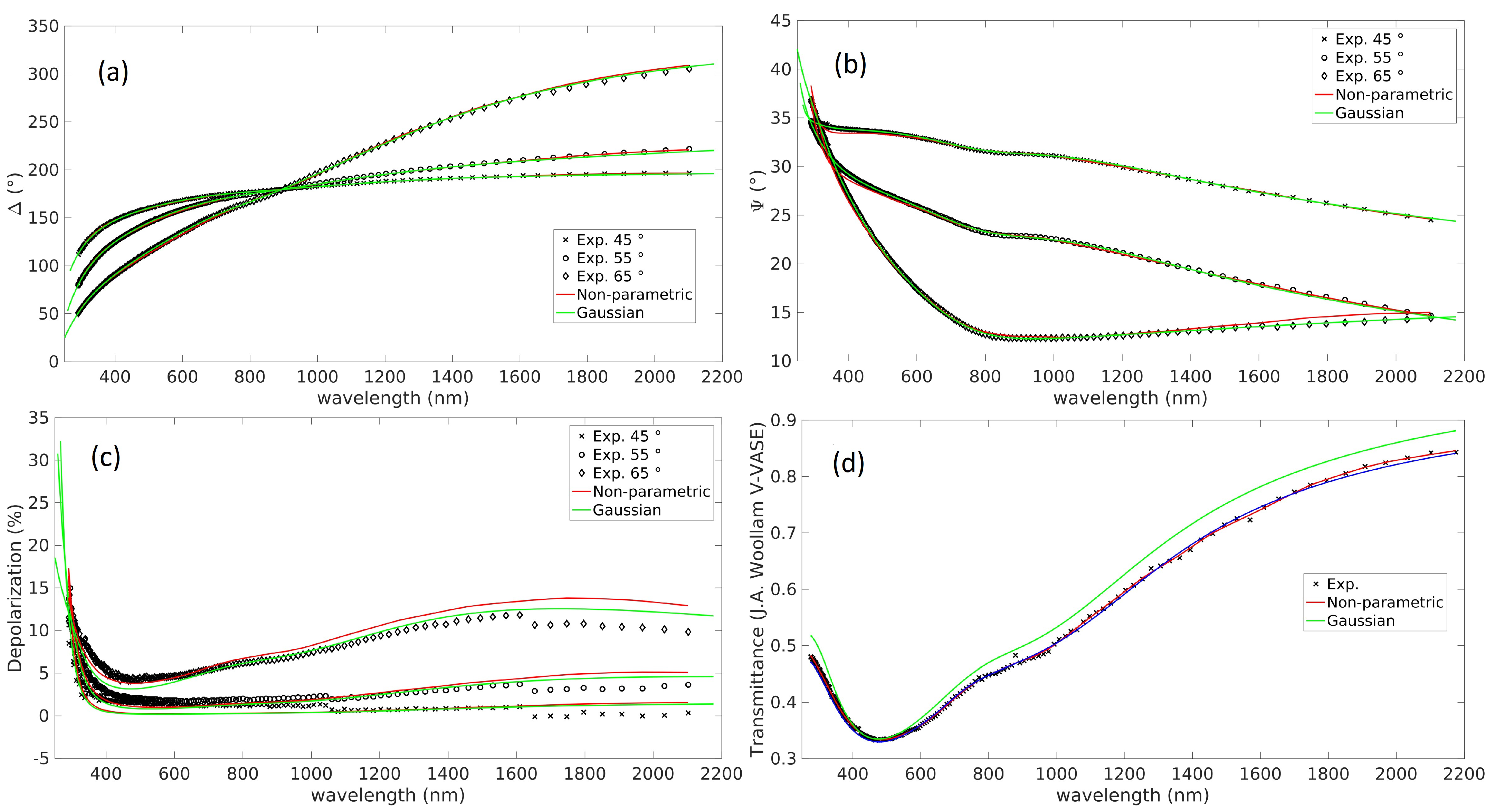
  • Non-parametric model: This approach is based on the assumption that the wavelength-dependencies of the real (n) and imaginary (k) part of the MIF effective refractive index are arbitrary smooth functions [14,22,24]. The discrepancy function to be minimized is:
    D F = 1 M q j y q n j , k j , d A l 2 O 3 , d M I F y ^ q , j σ q , j 2 + α 1 j n j 2 + α 2 j k j 2 ,
    where M is the total number of measurements, q is an index that runs over different types of spectra, j runs over wavelengths (or photon energy) of the spectra,  y q  is the computed spectra,  y ^ q , j  is the experimental data and  σ q , j  is the corresponding experimental uncertainty. The parameters  α 1  and  α 2  are regularization constants that control the smoothness of the optical constants dispersion and  n j  and  k j  are the second derivatives of the optical constants with respect to wavelength. The analysis has been performed using the OTF Studio software [31] taking into account spectra of ellipsometric angles  Δ  and  Ψ , depolarization degree and transmittance measured with the V-VASE ellipsometer.
  • Gaussian oscillators: The MIFs’ effective optical constants are modelled with a set of Gaussian oscillators, as described in [9]. The effective dielectric function assuming the contribution of N oscillators reads as:
    ϵ e f f E = ϵ + m = 1 N ϵ G R , m E + i ϵ G I , m E
    with
    ϵ G I , m E = A m e E E c , m B m 2 e E + E c , m B m 2
    ϵ G R , m E = 2 π p . v . 0 ξ ϵ G I , m ξ ξ 2 E 2 d ξ
    where E is the photon energy. The first term on the right-hand side of Equation (2),  ϵ , accounts for the polarization mechanisms that occur at photon energies above the measured spectral range. The second term is a sum of Gaussian oscillators that is used to model localized surface plasmon resonance and interband transitions. Each Gaussian oscillator is defined through its amplitude ( A m ), central energy ( E c , m ) and broadening ( B m ). In this case, the discrepancy function to be minimized is:
    D F = 1 M p q j y q A , B , E c , d A l 2 O 3 , d M I F y ^ q , j σ q , j 2 ,
    with p being the total number of parameters to be optimized,  A = { A 1 , A N } B = { B 1 , , B N }  and  E c = { E c , 1 , . . . , E c , N } . The analysis is performed with the WVASE software including the spectra of ellipsometric angles  Δ  and  Ψ , depolarization degree, and transmittance measured with the V-VASE ellipsometer.
  • β -do model: The  β -do model [18,19] essentially consists of a multiple-oscillator model where each oscillator is replaced by a  β  distribution in order to account for inhomogeneous line broadening. The dielectric function is then expressed as a sum over N oscillators:
    ϵ e f f E = ϵ + m = 1 N s = 1 P s w m , s χ m E s , E m w m , s
    with
    χ m E s , E = J m π 1 E s E i Γ m + 1 E s + E + i Γ m
    and
    w m , s = E s E m , m i n a m 1 E m , m a x E s b m 1 E m , m a x E m , m i n a m + b m 2
    In this case, the discrepancy function reads as
    D F = 1 M q j y q y ^ q , j σ q , j 2 + α 3 2 d M I F d ^ M I F d M I F + d ^ M I F 2 + α 4 2 d A l 2 O 3 d ^ A l 2 O 3 d A l 2 O 3 + d ^ A l 2 O 3 2 ,
    with  y q = y q J , Γ , E m i n , E m a x , a , b , d A l 2 O 3 , d M I F  being  J = { J 1 , , J N } Γ = { Γ 1 , , Γ N } E m i n = { E 1 , m i n , . . . , E N , m i n } E m a x = { E 1 , m a x , . . . , E N , m a x } a = { a 1 , , a N }  and  b = { b 1 , , b N } . The values  d ^ M I F  and  d ^ A l 2 O 3  correspond to the target thicknesses of the MIF and of the Al 2 O 3  layer. The analysis was done using a software developed by Steffen Wilbrandt for the analysis of spectrophotometric data. Reflectance and transmittance spectra measured with Lambda 25 and transmittance spectra measured with the V-VASE ellipsometer were used. It turns out that using only spectrophotometric data leads to a significant multiplicity of solutions and therefore it was often necessary to include weak bounds on the thickness values in the discrepancy function ( α 3 , α 4  0 in Equation (9)) to avoid non-physical solutions.

3. Results and Discussion

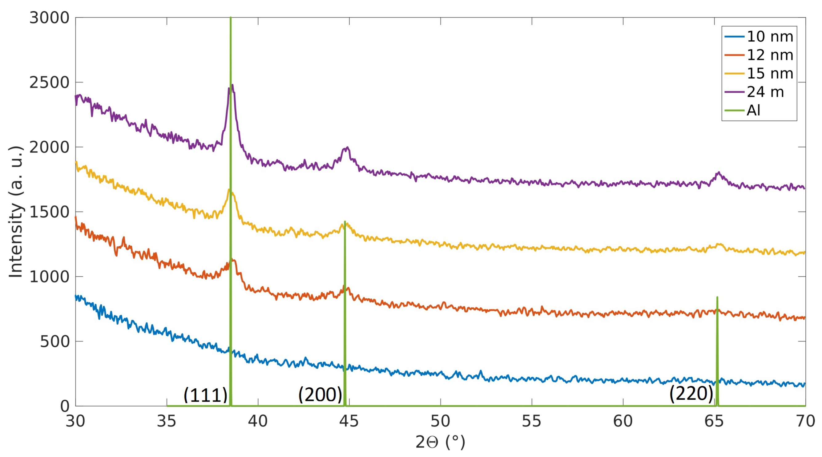
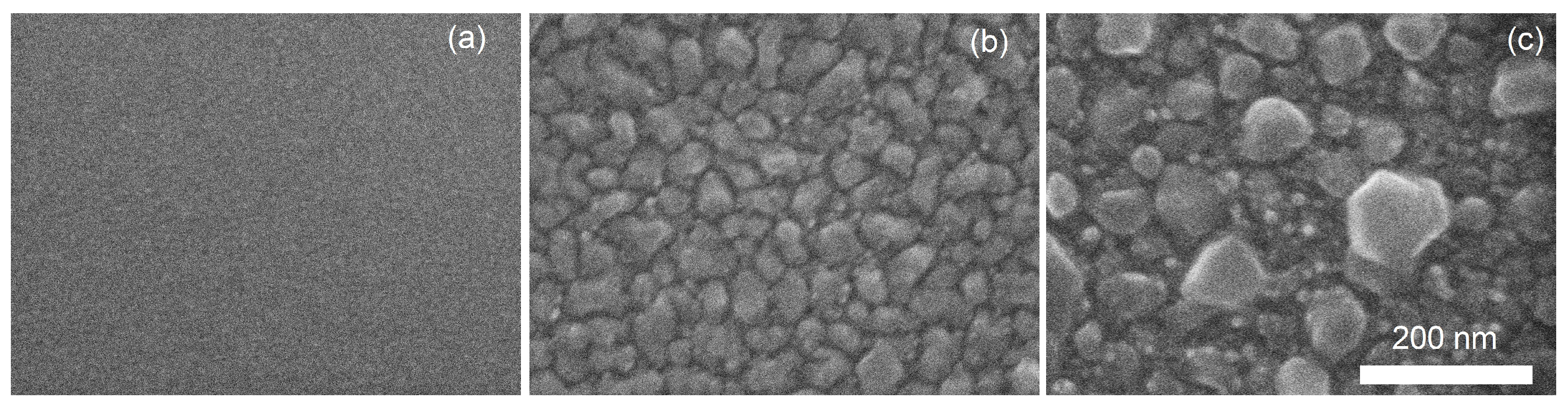
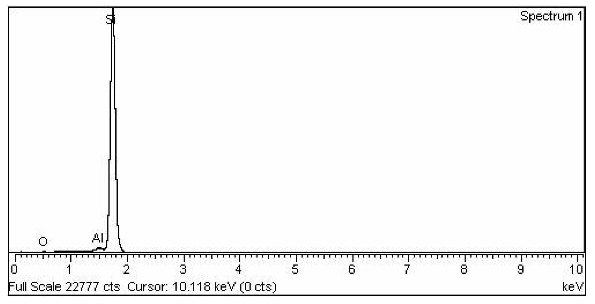
3.1. Structural Characterization

X-ray diffraction scans show the presence of an Al phase in metal island films and the diffraction peaks strength increases with the deposited mass thickness (Figure 1). Peaks intensities indicate that the Al nanoparticles are randomly oriented (no texture). XRD does not confirm the presence of Al for islands with  d A l ≤ 10 nm, suggesting either the presence of very small particles or the full oxidation of Al.
Scanning electron microscopy of samples deposited without the protective Al 2 O 3  coating is shown in Figure 2. For small mass thicknesses the island structure of the film can be hardly identified, indicating that the particle size should be below the resolution limit of the instrument (<10 nm). Increasing the mass thickness results in larger particles with sizes of several tens of nm for  d A l  = 24 nm and a broad particle size distribution with particle sizes up to cca. hundred nm for  d A l  = 32 nm. It should be noted the presence of bright spots at the particle edges and vertices that are indicative of charging effects and suggest preferential locations for Al oxidization. EDS measurements confirmed the presence of Al and O on the sample surface, in addition to the Si signal from the substrate (Figure 3).

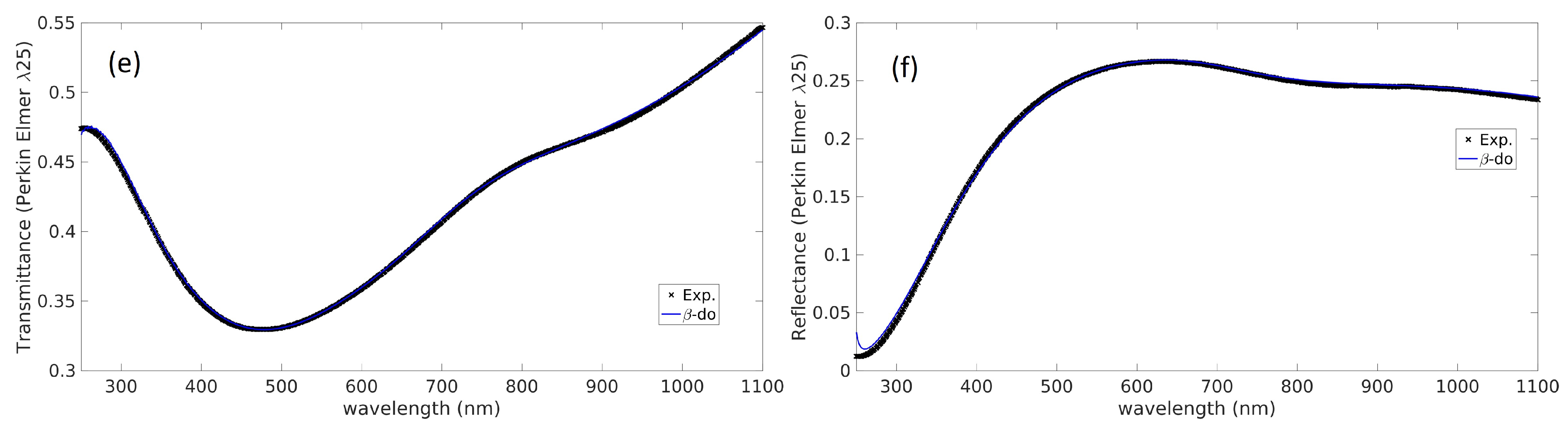
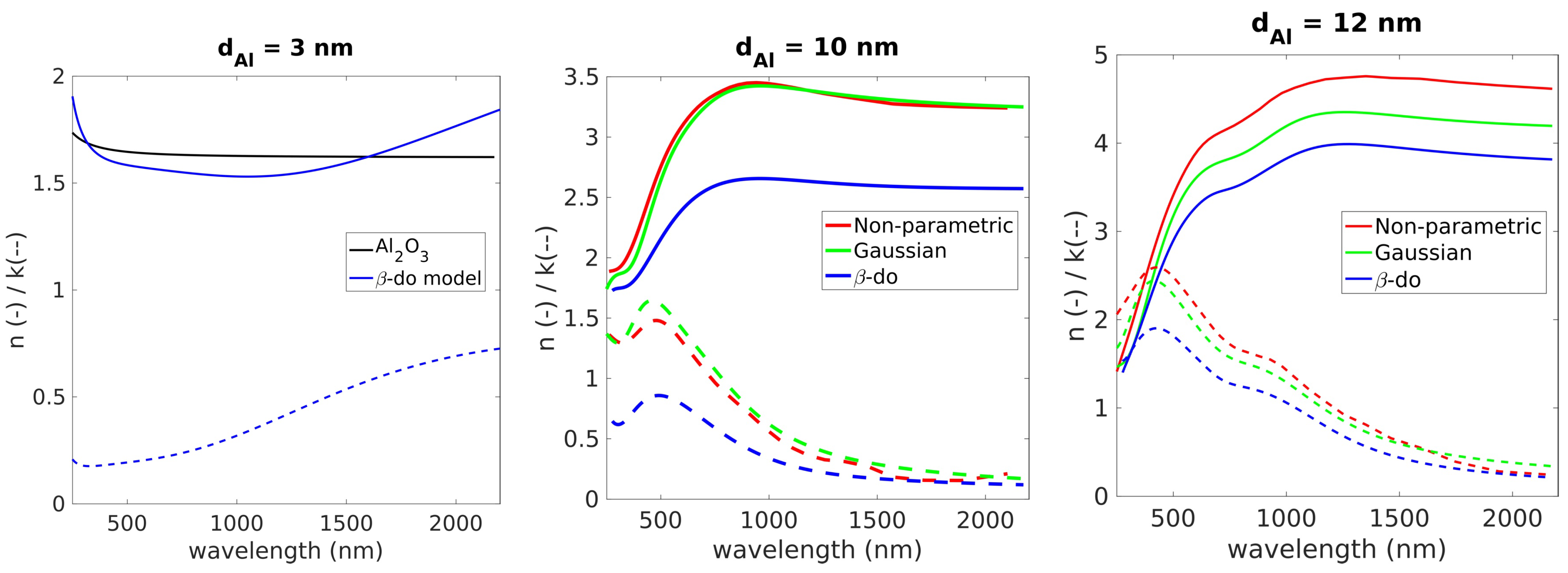
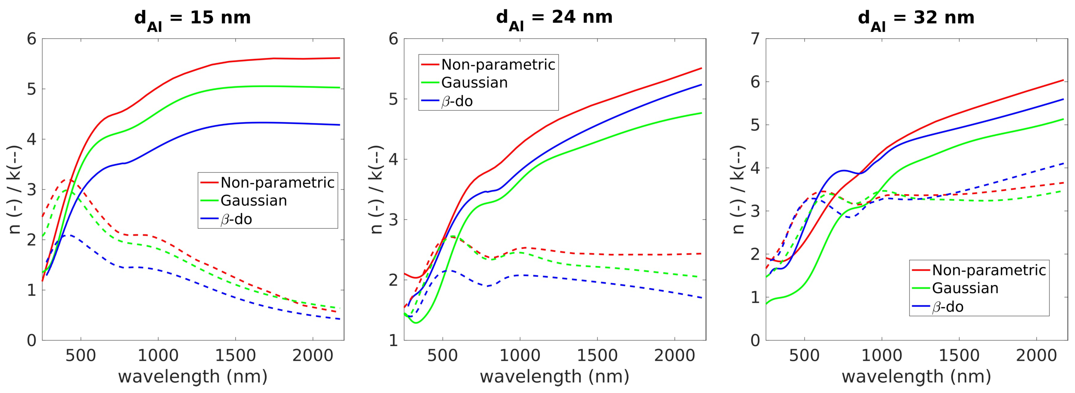
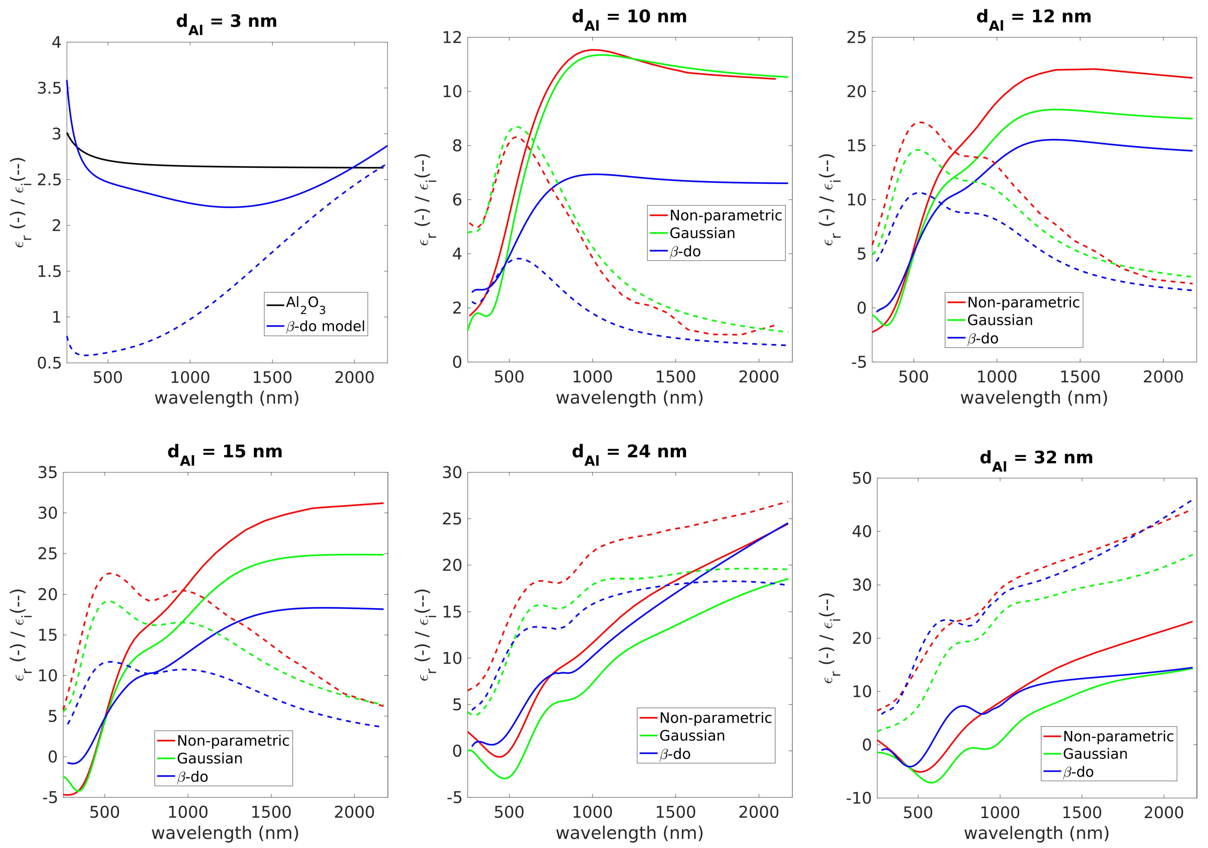
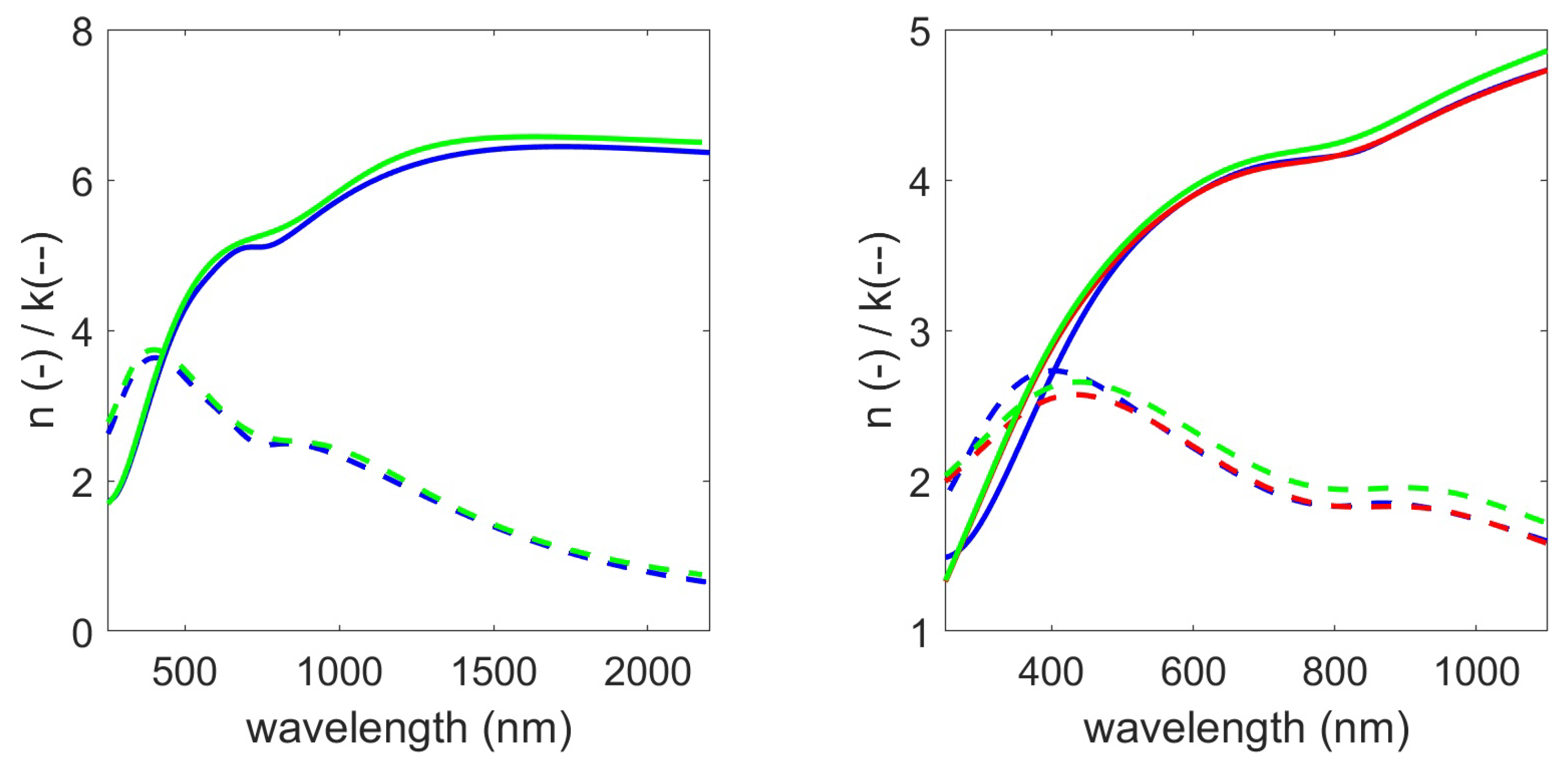
3.2. Optical Characterization

All the used approaches provided a remarkable agreement between the experimental data and the data computed from the models, as shown in Figure 4 for the sample with  d A l  = 12 nm. The resulting thickness values for the Al island film and the Al 2 O 3  overlayer are displayed in Table 1. Note that for the sample with  d A l  = 10 nm, two results are presented for the  β -do model, the one displayed in the right column corresponding to the result obtained with no thickness regularization ( α 3  =  α 4  = 0). In general terms,  d M I F  monotonically increases with the deposited Al mass thickness while no obvious trend is observed for the  d A l 2 O 3 , yet it displays values larger than the Al 2 O 3  deposited mass thickness. The effective values of Al 2 O 3  layers thicknesses might significantly differ from the deposited mass thickness. On one hand, a fraction of deposited Al 2 O 3  can fill the space between Al islands, being effectively incorporated in the MIF layer. On the other hand, partial oxidation of Al islands, especially the outermost regions, can result in a larger overall amount of Al 2 O 3  in the sample. Thus, these non-idealities have opposite effects on  d A l 2 O 3  and the magnitude of the discrepancy with respect to the deposited mass thickness can not be easily predicted in advance. Since the inferred thicknesses are larger than the deposited ones, partial oxidation of Al island film seems to take place. This observation is in accordance with the fact that the thinnest MIF seems to be fully oxidized.
For the sample with  d A l  = 3 nm, the non-parametric approach and the Gaussian oscillator modelling results in  d M I F  = 0 nm, suggesting that the Al layer is fully oxidized. On the other hand, modelling based on the  β -do oscillator provides  d M I F  = 3 nm. However, the optical constants of the metal island film in this case are very close to those of Al 2 O 3 , as shown in Figure 5. The increased imaginary part of the refractive index can be attributed to the non-stoichiometric oxidation of the MIF. For samples with a moderate mass thickness (10 nm ≤  d A l  ≤ 15 nm), the effective optical constants line-shape reflect the typical response of a film consisting of isolated nanoparticles, dominated by the localized plasmon resonance and with a near-infrared shoulder that can be associated to the interband transitions in Al [28]. Overall, a progressive shift of the main peak of the imaginary part of the effective dielectric function (Figure 6) to longer wavelengths is observed when increasing  d A l , which can be associated with the red-shift of the localized surface plasmon resonance of Al islands. The samples with larger Al mass thicknesses values ( d A l  ≥ 24 nm) display enhanced optical losses in the infrared range, suggesting the contribution of clustered nanoparticles [12]. However, the results were not improved if a Drude-like term was included in the multiple oscillator approaches ( β -do and Gaussian), indicating that the percolation regime was not achieved.
It should be noted that the non-parametric approach does not assume a causal relation between the real and imaginary parts of the complex refractive index of the metal island film, i.e., it does not impose Kramers-Kronig consistency. However, the dispersion line-shape obtained with this approach resembles, in general, the ones of the multiple-oscillator approaches. We have verified that the optical constants dispersion that results from this approach can be well-fitted in all cases by a sum of several Gaussian or Lorentzian oscillators, confirming that the obtained solution is physically sound. The larger qualitative discrepancies are found for the samples with larger mass thickness i.e., those with larger optical losses in the infrared range, particularly the one with  d A l  = 32 nm. In this case, the refractive index (and the real part of the dielectric function) of the non-parametric model presents a smoother dispersion than the oscillators-based models, which display a dip at ≈1000 nm. The non-parametric model turns out to be more flexible to describe the spectral range between visible and infrared absorption regions because it treats independently real and imaginary parts of the optical constants. Thus, the imaginary part can present a dip between these regions while the real part smoothly varies. On the other hand, the oscillator-based models must display a dip in the real part in order to properly account for the dip in the imaginary part.
In all cases, the  β -do model required the use of 3 oscillators to provide a satisfactory data fit, while the number of necessary Gaussian oscillators was between 3 and 7 depending on the sample. It means that for some samples the total number of parameters to be optimized was larger for the Gaussian model than for the  β -do model. In the case of highly inhomogeneous line-broadening, several Gaussian oscillators were needed to provide the asymmetry of a single  β -do oscillator. On the other hand, if the line-broadening was moderately inhomogeneous, one or two Gaussian oscillators were sufficient to provide a good description of a single resonance.
Although the optical constants dispersion line-shape for each sample is similar for all the approaches, the refractive index values appear to be shifted by a nearly constant value. It can be observed that the larger refractive index values are associated with smaller values of  d M I F  due to the strong correlation of refractive index and thickness for very thin layers [32]. Thus, the same optical thickness can result on different combinations of refractive index and layer thickness for different approaches. It has been suggested that the combination of spectroscopic ellipsometry and photometric measurements enforces refractive index/thickness solution uniqueness in the case of very thin absorbing films [33]. Nevertheless, in the present case, where the characterization of two very thin films (MIF and Al 2 O 3 ) has to be addressed, a multiplicity of solutions can be found.
In this context, it can be questioned whether the observed differences arise from using alternative dispersion models or due to the fact that distinct data sets are employed in each case. We have performed the characterization of the sample with  d A l  = 15 nm with the  β -do and Gaussian oscillator models using only spectrophotometric data and assuming no bounds in thickness ( α 3  =  α 4  = 0 in Equation (9)). In this case, both approaches lead to virtually the same results ( d M I F  = 6.5 nm and  d A l 2 O 3  = 23.1 nm for the Gaussian oscillators,  d M I F  = 6.8 nm and  d A l 2 O 3  = 24.3 nm for the  β -do model) with nearly identical optical constants dispersion (Figure 7 left). The non-parametric approach could not be reliably applied to the analysis of the data in the range above 1100 nm since only transmittance data is available in that range and both optical constants n and k can not be determined. Hence, we also compare the characterization results for all approaches using spectrophotometric data in the range 250–1100 nm. In this case, the optimal layer thickness was very unstable and was fixed to  d M I F  = 11.2 nm. In that case, all the used approaches lead to almost the same optical constants (Figure 7 right), indicating that different dispersion modelling approaches can be equivalent if the same experimental data set is used.

4. Conclusions

Different approaches have been applied to the optical characterization of Al thin films deposited by electron beam evaporation: a non-parametric model and two multiple-oscillator models based on Gaussian and  β -distributed oscillators. A remarkable agreement between experimental data and simulations is achieved in all the cases.
All models enable deducing the same trends (increase in effective thicknesses, red-shift and broadening of the localized plasmon resonance, increase of optical losses in the infrared range) for the evolution of the effective optical response of the island films as a function of the deposited Al mass thickness. Therefore, similar physical insights can be extracted regardless of the used modelling approach.
The values of effective thickness and optical constants significantly depend on the used approach. These parameters are of critical importance for the practical incorporation of metal island films in optical coatings and the observed diversity of solutions is a serious limiting factor.
We have verified that upon the use of equivalent discrepancy functions and experimental data sets, the different approaches reliably tend towards a similar solution. In this sense, the most crucial factor appears to be the use of a reliable set of experimental data. In that case, all of the used models would provide very similar solutions.
Therefore this round-robin optical characterization study brings insights for understanding the advantages (consistent physical interpretation of sample evolution with mass thickness) and limitations (multiplicity of solutions enhanced by the use of different data sets) of optical characterization of metal island films overcoated with thin dielectric layers.

Author Contributions

Conceptualization, J.S.-P., V.J. and O.S.; methodology, all; software, S.W. and M.T.; validation, J.S.-P., T.A. and S.W.; formal analysis, all; investigation, all; resources, J.S.-P.; data curation, H.K. and J.S.-P.; writing—original draft preparation, J.S.-P., T.A. and S.W.; writing—review and editing, all.; visualization, J.S.-P., T.A., S.W. and H.K.; supervision, J.S.-P.; project administration, J.S.-P.; funding acquisition, J.S.-P. All authors have read and agreed to the published version of the manuscript.

Funding

This research was partially funded by the Croatian Science Foundation through the projects IP-2019-04-5424 and DOC-2021-02-7236 and the Fraunhofer internal project Multi-KID (Grant No. 601001).

Data Availability Statement

The data presented in this study are available on request from the corresponding author.

Conflicts of Interest

The authors declare no conflict of interest. The funders had no role in the design of the study; in the collection, analyses, or interpretation of data; in the writing of the manuscript; or in the decision to publish the results.

References

  1. Kaiser, N. Review of the fundamentals of thin-film growth. Appl. Opt. 2002, 41, 3053–3060. [Google Scholar] [CrossRef] [PubMed]
  2. Stenzel, O.; Macleod, A. Metal-dielectric composite optical coatings: Underlying physics, main models, characterization, design and application aspects. Adv. Opt. Technol. 2012, 1, 463–481. [Google Scholar] [CrossRef] [Green Version]
  3. Ghobadi, A.; Ghobadi, T.G.U.; Ozbay, E. Lithography-free metamaterial absorbers: Opinion. Opt. Mater. Express 2022, 12, 524–532. [Google Scholar] [CrossRef]
  4. Janicki, V.; Amotchkina, T.V.; Sancho-Parramon, J.; Zorc, H.; Trubetskov, M.K.; Tikhonravov, A.V. Design and production of bicolour reflecting coatings with Au metal island films. Opt. Express 2011, 19, 25521–25527. [Google Scholar] [CrossRef] [PubMed] [Green Version]
  5. Yu, R.; Mazumder, P.; Borrelli, N.F.; Carrilero, A.; Ghosh, D.S.; Maniyara, R.A.; Baker, D.; García de Abajo, F.J.; Pruneri, V. Structural coloring of glass using dewetted nanoparticles and ultrathin films of metals. ACS Photo. 2016, 3, 1194–1201. [Google Scholar] [CrossRef] [Green Version]
  6. Nath, J.; Smith, E.; Maukonen, D.; Peale, R.E. Optical Salisbury screen with design-tunable resonant absorption bands. J. Appl. Phys. 2014, 115, 193103. [Google Scholar] [CrossRef] [Green Version]
  7. Li, Z.; Butun, S.; Aydin, K. Large-area, lithography-free super absorbers and color filters at visible frequencies using ultrathin metallic films. ACS Photo. 2015, 2, 183–188. [Google Scholar] [CrossRef] [Green Version]
  8. Willey, R.R.; Stenzel, O. Designing Optical Coatings with Incorporated Thin Metal Films. Coatings 2023, 13, 369. [Google Scholar] [CrossRef]
  9. Sancho-Parramon, J.; Janicki, V.; Zorc, H. On the dielectric function tuning of random metal-dielectric nanocomposites for metamaterial applications. Opt. Express 2010, 18, 26915–26928. [Google Scholar] [CrossRef] [Green Version]
  10. Held, M.; Stenzel, O.; Wilbrandt, S.; Kaiser, N.; Tünnermann, A. Manufacture and characterization of optical coatings with incorporated copper island films. Appl. Opt. 2012, 51, 4436–4447. [Google Scholar] [CrossRef]
  11. Biegański, P.; Dobierzewska-Mozrzymas, E.; Kępiński, L. Application of effective medium theory with consideration of island shapes to interpret optical properties of discontinuous Pt films. Appl. Opt. 2012, 51, 6945–6951. [Google Scholar] [CrossRef] [PubMed]
  12. de Vries, A.J.; Kooij, E.S.; Wormeester, H.; Mewe, A.A.; Poelsema, B. Ellipsometric study of percolation in electroless deposited silver films. J. Appl. Phys. 2007, 101, 053703. [Google Scholar] [CrossRef]
  13. Hövel, M.; Gompf, B.; Dressel, M. Dielectric properties of ultrathin metal films around the percolation threshold. Phys. Rev. B 2010, 81, 035402. [Google Scholar] [CrossRef] [Green Version]
  14. Amotchkina, T.V.; Janicki, V.; Sancho-Parramon, J.; Tikhonravov, A.V.; Trubetskov, M.K.; Zorc, H. General approach to reliable characterization of thin metal films. Appl. Opt. 2011, 50, 1453–1464. [Google Scholar] [CrossRef] [Green Version]
  15. Sancho-Parramon, J.; Janicki, V.; Zorc, H. Tuning the effective dielectric function of thin film metal-dielectric composites by controlling the deposition temperature. J. Nanophoto. 2011, 5, 051805. [Google Scholar] [CrossRef] [Green Version]
  16. Lončarić, M.; Sancho-Parramon, J.; Zorc, H. Optical properties of gold island films—A spectroscopic ellipsometry study. Thin Solid Film. 2011, 519, 2946–2950. [Google Scholar] [CrossRef]
  17. Brendel, R.; Bormann, D. An infrared dielectric function model for amorphous solids. J. Appl. Phys. 1992, 71, 1–6. [Google Scholar] [CrossRef]
  18. Wilbrandt, S.; Stenzel, O. Empirical extension to the multioscillator model: The beta-distributed oscillator model. Appl. Opt. 2017, 56, 9892–9899. [Google Scholar] [CrossRef]
  19. Stenzel, O.; Wilbrandt, S. Beta-distributed oscillator model as an empirical extension to the Lorentzian oscillator model: Physical interpretation of the β_do model parameters. Appl. Opt. 2019, 58, 9318–9325. [Google Scholar] [CrossRef]
  20. Wilbrandt, S.; Stenzel, O.; Liaf, A.; Munzert, P.; Schwinde, S.; Stempfhuber, S.; Felde, N.; Trost, M.; Seifert, T.; Schröder, S. Spectrophotometric Characterization of Thin Semi-Transparent Aluminum Films Prepared by Electron Beam Evaporation and Magnetron Sputtering. Coatings 2022, 12, 1278. [Google Scholar] [CrossRef]
  21. Stenzel, O.; Wilbrandt, S.; He, J.Y.; Stempfhuber, S.; Schröder, S.; Tünnermann, A. A Model Surface for Calculating the Reflectance of Smooth and Rough Aluminum Layers in the Vacuum Ultraviolet Spectral Range. Coatings 2023, 13, 122. [Google Scholar] [CrossRef]
  22. Stenzel, O.; Petrich, R. Flexible construction of error functions and their minimization: Application to the calculation of optical constants of absorbing or scattering thin-film materials from spectrophotometric data. J. Phys. Appl. Phys. 1995, 28, 978. [Google Scholar] [CrossRef]
  23. Djurišić, A.B.; Chan, Y.; Li, E.H. Progress in the room-temperature optical functions of semiconductors. Mater. Sci. Eng. Rep. 2002, 38, 237–293. [Google Scholar] [CrossRef]
  24. Amotchkina, T.V.; Trubetskov, M.K.; Tikhonravov, A.V.; Janicki, V.; Sancho-Parramon, J.; Zorc, H. Comparison of two techniques for reliable characterization of thin metal–dielectric films. Appl. Opt. 2011, 50, 6189–6197. [Google Scholar] [CrossRef] [PubMed] [Green Version]
  25. Franklin, D.; He, Z.; Mastranzo Ortega, P.; Safaei, A.; Cencillo-Abad, P.; Wu, S.T.; Chanda, D. Self-assembled plasmonics for angle-independent structural color displays with actively addressed black states. Proc. Natl. Acad. Sci. USA 2020, 117, 13350–13358. [Google Scholar] [CrossRef]
  26. McPeak, K.M.; Jayanti, S.V.; Kress, S.J.; Meyer, S.; Iotti, S.; Rossinelli, A.; Norris, D.J. Plasmonic films can easily be better: Rules and recipes. ACS Photo. 2015, 2, 326–333. [Google Scholar] [CrossRef]
  27. Nguyen, H.V.; An, I.; Collins, R. Evolution of the optical functions of thin-film aluminum: A real-time spectroscopic ellipsometry study. Phys. Rev. B 1993, 47, 3947. [Google Scholar] [CrossRef]
  28. Nguyen, H.V.; An, I.; Collins, R. Evolution of the optical functions of aluminum films during nucleation and growth determined by real-time spectroscopic ellipsometry. Phys. Rev. Lett. 1992, 68, 994. [Google Scholar] [CrossRef]
  29. Dobrowolski, J.; Ho, F.; Waldorf, A. Determination of optical constants of thin film coating materials based on inverse synthesis. Appl. Opt. 1983, 22, 3191–3200. [Google Scholar] [CrossRef]
  30. Palik, E.D. Handbook of Optical Constants of Solids; Academic Press: Cambridge, MA, USA, 1998; Volume 3. [Google Scholar]
  31. Trubetskov, M. OTF Studio Software. Available online: https://www.otfstudio.com (accessed on 4 May 2023).
  32. Arwin, H.; Aspnes, D.E. Unambiguous determination of thickness and dielectric function of thin films by spectroscopic ellipsometry. Thin Solid Film. 1984, 113, 101–113. [Google Scholar] [CrossRef]
  33. Hilfiker, J.N.; Singh, N.; Tiwald, T.; Convey, D.; Smith, S.M.; Baker, J.H.; Tompkins, H.G. Survey of methods to characterize thin absorbing films with spectroscopic ellipsometry. Thin Solid Film. 2008, 516, 7979–7989. [Google Scholar] [CrossRef]
Figure 1. X-ray diffraction scans for Al island films with different mass thicknesses. Green lines correspond to pure fcc-Al phase (JCPDS Card No. 03-065-2869).
Coatings 13 01073 g001
Figure 2. Scanning electron microscopy picture of bare Al islands (not coated with Al 2 O 3 ) having a mass thickness equal to 15 (a), 24 (b) and 32 nm (c).
Coatings 13 01073 g002
Figure 3. EDS measurements of the surface of the sample with Al island film (not coated with Al 2 O 3 ) having a mass thickness equal 24 nm.
Coatings 13 01073 g003
Figure 4. Fits of experimental data (black symbols) of the sample with  d A l  = 12 nm obtained by the three modelling approaches employed in the study: non-parametric approach (red lines), Gaussian oscillators (green lines),  β -do model (blue lines). Data corresponds to ellipsometric angles  Δ  (a) and  Ψ  (b), depolarization (c), transmittance measured with the J.A. Woollam V-VASE ellipsometer (d), transmittance (e) and reflectance (f) measured with the Perkin Elmer  λ 25 spectrophotometer.
Coatings 13 01073 g004aCoatings 13 01073 g004b
Figure 5. Effective refractive index (solid lines) and extinction coefficient (dashed lines) of the metal island film layer for films with different mass thickness.
Coatings 13 01073 g005aCoatings 13 01073 g005b
Figure 6. Real (solid lines) and imaginary (dashed lines) parts of the effective dielectric function of the metal island film layer for films with different mass thickness.
Coatings 13 01073 g006
Figure 7. Effective refractive index (solid lines) and extinction coefficient (dashed lines) of the metal island film layer for the sample with  d A l  = 15 nm using different approaches (red—parameter free dispersion, green—Gaussian oscillators, blue— β -do model) and only spectrophotometric data in the whole spectral range (left) and in the spectral range 250–1100 nm (right).
Coatings 13 01073 g007
Table 1. Thickness for Al metal island film ( d M I F ) and Al 2 O 3  overlayer ( d A l 2 O 3 ) as determined by the different approaches employed in this study.
d Al  (nm)31012152432
Non-parametric model d M I F  (nm)04.58.79.119.825.8
d A l 2 O 3  (nm)20.020.228.225.826.121.4
Gaussian oscillators d M I F  (nm)04.610.811.426.434.5
d A l 2 O 3  (nm)19.915.925.723.316.810.1
β -do d M I F  (nm)3.09.8      23.313.916.825.927.2
d A l 2 O 3  (nm)15.014.6      8.023.419.019.219.6
Disclaimer/Publisher’s Note: The statements, opinions and data contained in all publications are solely those of the individual author(s) and contributor(s) and not of MDPI and/or the editor(s). MDPI and/or the editor(s) disclaim responsibility for any injury to people or property resulting from any ideas, methods, instructions or products referred to in the content.

