Review

Microstructured All-Optical Switching Based on Two-Dimensional Material

1
School of Physics and Electronics, Hunan Normal University, Changsha 410081, China
2
Institute of Mathematics and Physics, Central South University of Forestry and Technology, Changsha 410004, China
*
Authors to whom correspondence should be addressed.
Coatings 2023, 13(5), 876; https://doi.org/10.3390/coatings13050876
Submission received: 28 February 2023 / Revised: 11 March 2023 / Accepted: 20 March 2023 / Published: 6 May 2023
(This article belongs to the Special Issue Optical Properties of Crystals and Thin Films)

Abstract

:
Microstructured all-optical switching, possessing the unique function of light controlling light, is an important part of the on-chip ultra-fast optical connectivity network and integrated logic computing chip. Microstructured all-optical switching has attracted extensive research interest, the latest great developments of which have also yielded progress in nanophotonics, nonlinear optics, optical communications, and integrated optics, etc. The emergence of two-dimensional materials with good third-order optical nonlinearity provides an important driving force for the improvement of all-optical switches. This paper reviews the implementation principles, novel configurations, improved performance indexes, and research progress based on different two-dimensional materials for micro/nano all-optical switching. Not only is a systematic discussion of the current state provided, but also, a brief outlook is afforded on the remaining challenges in the pursuit of the application of practical on-chip microstructured all-optical switching that is based on two-dimensional materials.

1. Introduction

Micro/nano-scale all-optical devices are considered the core of next-generation ultrafast communication and signal processing systems. In the current phase of photoelectric hybrids, all-optical switching technology must be developed to break through the bottleneck of information exchange. As the core component, all-optical switches play a crucial role in building on-chip ultrafast all-optical switch networks [1]. All-optical switching is a device based on the light-controlled-by-light concept, which can convert or logically operate the optical signals in an optical transmission line or integrated optical circuit. The all-optical switch uses fast optical nonlinearity to achieve a fast and reversible transition from one state to another for a parameter of the optical signal, such as power, phase, frequency, and polarization, etc. [2]. This lays the foundation for optical computing systems, optical communication networks, and quantum information processing chips [3]. Therefore, controlling photons on the micro–nano scale and developing all-optical devices with a smaller size and better performance have become a hot spot in the international research frontier, as well as in regard to competition with new technologies.
Because of the scientific importance and practical application of all-optical switching, it has been conducted for a long time, even dating back to the study of optical bistability in 1965 and also the experimental demonstration of optical bistability in 1976 [4]. However, the nonlinear refractive index of conventional materials is small and the ohmic loss of metallic materials is large. These material bottleneck limitations constitute a major obstacle to all-optical switching. Although optical nonlinearities are related to optical matter interactions enhanced by microstructures (including microcavities) and optical nonlinearities enhanced by slow-light effects, it is still difficult to achieve nanoscale all-optical switching with ultra-high speed, ultra-low energy consumption, and ultra-high switching efficiency is still difficult to implement [1]. In addition, large nonlinear magnetization rates and ultra-fast response times are difficult to achieve simultaneously for conventional third-order optically nonlinear materials, including semiconductors, polymers, and liquid crystals, even in previously reported microphotonic devices, where light–matter interactions and subsequent optical nonlinearities are typically weak [5,6,7]. This also limits the use of optical third-order nonlinear materials in the context of all-optical switching.
In fact, in addition to many traditional third-order nonlinear materials, many new materials have been investigated. Recent studies have shown that two-dimensional materials have great potential for achieving ultrafast all-optical switching. The remarkable optical properties of two-dimensional materials make them promising for important applications in nanophotonics. In this review, we discuss recent advances in microstructured all-optical switching based on two-dimensional materials, including the special strategies to address inherent barriers and fundamental challenges for ultrafast nanoscale on-chip triggered all-optical switching. The basic principles, performance indicators, and novel two-dimensional materials for realizing ultrafast all-optical switches are reviewed. In addition to this, the current research challenges are briefly anticipated, as well as the development directions and future prospects of microstructured all-optical switching that are based on two-dimensional materials.

2. Basic Concepts and Realization Principles

All-optical switching is based on nonlinear optics, which generally occur when the optical field that is associated with one or more laser beams propagating in a material are large enough to produce a polarization field that is directly proportional to the product of two or more incident optical fields [8,9]. All-optical switching based on a nonlinear principle operates directly in the optical domain without photoelectric conversion [10], resulting in high efficiency, low switching noise, low loss [11,12], and switching speeds that are of nanoseconds, picoseconds, or even less [13]. However, since photons are not charged, it is not possible to control light by light directly, as the case in electronics; only nonlinear optical indirect methods can be used. With an external beam of strong light (controllable pump), or by the intense light of the signal light itself (self-pumped), and the propagation of the signal light–medium interaction, only then does its optical properties undergo nonlinear changes. The changes, such as absorption or refraction of the medium (the imaginary or real part of susceptibilities), occur depending on the change in optical power, so as to control the signal light wave vector, phase, or polarization, thus resulting in finally achieving control of the intensity (amplitude) or propagation direction of the signal light [14]. For instance, the phase shift is given by Equation (1):
Δ φ = 2 π Δ n F L / λ
where F accounts for any cavity resonance enhancement, light travels a distance L, and the change in the refractive index of light is Δ n . All-optical switches are based on a variety of different nonlinear mechanisms. The main nonlinear mechanisms and corresponding switching principles are briefly listed in the Table 1 [15]:
There are many kinds of all-optical switches and ways in which to realize them. These include the optical bistable all-optical switching [4,16,17], the optical limiting all-optical switch [18], the nonlinear interferometer all-optical switching (UNI) [19], the nonlinear grating all-optical switching [20], the nanophotonics all-optical switch [2,21], and other all-optical switching. In conclusion, all-optical switching is a device that changes the intensity or propagation direction of controlled light by controlling the nonlinear optical effect of light on the medium. Furthermore, it is a key technology and important device for future optical computing systems, as well as high-speed all-optical communication networks.
All-optical switching is based on the spatial or temporal nonlinear response of the material [18,22]. Practical all-optical switching devices can use photonic (or plasmonic) micro/nano-structures as a matrix, combined with optical nonlinear materials. Nonlinear optical microstructures (including nonlinear photonic crystals (PhCs), PhC nanocavities [23,24], nonlinear dielectric ring nanocavities side-coupled bus signal waveguides [25], etc.), nonlinear plasmonic structure-like nonlinear plasmonic nanocavities [26], and nonlinear metamaterials/super surfaces [27], etc., are widely used to construct all-optical switching. The basic implementation mechanism of all-optical switching is the nonlinear Kerr effect, which can be defined as a light-induced double refraction or the intensity-dependent refractive index. The refractive index of nonlinear material can be obtained by using the nonlinear Kerr effect [28]:
n = n 0 + n 2 I
where n0 is the linear refractive index, n2 is the nonlinear part, and I is the intensity of the control light.

2.1. Photonic Crystal All-Optical Switching

In the past few decades, photonic crystals have become a rapidly growing field in quantum physics and micro-optics. One of its major characteristics is that it can control the propagation of photons and is the host of various new optical nonlinear effects [29]. PhCs are artificial microstructures with a spatially periodic dielectric distribution. The periodic distribution of the refractive index can produce a photonic band gap (also called the stop band) in photonic crystals. No photon can pass through the photonic band gap, and the incident signal light is completely reflected [30]. If the periodic characteristics of PhCs are destroyed by introducing defects, corresponding defect energy levels will be formed in the photonic band gap. Only light with a specific frequency can appear in this defective energy level. Changes in the permittivity of nonlinear materials change the spatially periodic refractive index distribution of photonic crystals, leading to changes in the photonic crystal band structure. Switching photonic bandgap crystals provides dynamic control of the density of states, which will allow switching on or off of the light source in the bandgap [31]. In addition, the photonic crystal structure can have an infinite number of arrangement forms, which makes it possible to realize the all-off switch that is based on photonic crystals [32]. All-optical switching based on a silicon chip is realized in photonic crystal nanocavities (~50 ps) [33]. For example, Takasumi et al. proved that all-optical switches on a silicon chip were realized by photonic crystal nanocavities at a high speed (~50 ps). D. Nau et al. discussed the optical switching of metallic photonic crystal slabs with a photochromic polymer [34]. Kengo et al. demonstrated low-energy all-optical switching by using a combination of photonic crystal nanocavities and strong carrier-induced nonlinearity in InGaAsP [2]. Zhao et al. demonstrated an ultrafast optical switching based on photonic molecule–waveguide coupling in a photonic crystal plate structure [35].

2.2. All-Optical Switching Based on Dielectric Ring Nanocavities

By coupling the bus signal waveguide on the side, the dielectric ring nanocavity can be used to build all-optical switching devices [25]. As we all know, the resonant mode is very sensitive to the dielectric constant. Due to the optical Kerr effect of nonlinear materials, the dielectric constant can be changed by the pump light. In addition, the signal light can be selected at the nanocavity mode center. Then, the incident light is coupled into the nano-cavity through the coupling aisle. No signal light can be transmitted through the bus signal waveguide, which corresponds to the OFF state of the all-optical switching. The nanocavity mode of the controlled optical pumping deviates from the signal light wavelength, and the energy coupling between the signal light and the nanocavity mode is cut off, corresponding to the ON state of the all-optical switching. Therefore, the all-optical switch function is formed by coupling a dielectric ring nano-cavity and a side bus signal waveguide.

2.3. Plasmonic All-Optical Switching

Recently, surface plasmon polaritons (SPPs) have been found to provide an alternative way by which to achieve strong nonlinear optical effects, as well as to minimize all-optical components due to its significantly enhanced optical field strength and light manipulation in a nanoscale domain [36,37,38]. Surface plasmonpolaritons (SPPs), a concept of surface waves, are formed by the combined action of electron oscillations and incident photons, which are located at the interface of two different media with opposite signs of the real part of the dielectric constant [39]. For extended metal surfaces, this means that SPPs are surface electromagnetic wave-propagation modes occurring between metal dielectric interfaces. For metals in nanoparticles, the response yields local electromagnetic wave oscillation modes (surface electromagnetic wave propagation modes), which indicate the presence of local SPPs. In this context, many new physical concepts have been proposed, including metamaterials, plasmonic nanoparticles, and plasmonic PhCs, etc. Plasmonic nanostructures have small feature sizes in the order of hundreds of nanometers, as well as possess the unique property of limiting light intensity to the subwave length range, and have tremendous near-field enhancement [40].
In recent years, several nonlinear optical devices based on SPPs have been investigated [41,42,43,44,45]. Compared with dielectric nanostructures, plasmonic nanostructures have stronger optical-confinement and field-enhancement effects, which are suitable for achieving all-optical switching. Three factors make SPPs an excellent candidate for achieving ultra-low and ultra-fast all-optical switching. First, SPPs can enhance the interaction between light and matter due to its powerful local enhancement effect, as this reduces the pump intensity. Second, changes in the dielectric constant of the ambient medium can greatly affect the resonant response of SPPs. A small change in the surrounding material index can produce a large change in the resonance properties [46], which can also reduce the pump energy consumptions. Finally, the relaxation time of the plasmon resonance can reach the sub-picoseconds level, which can ensure ultra-fast all-optical switching. This makes it feasible to build all-optical switching devices using plasmonic nanostructures. In the presence of controlled light, the refractive index of the ambient medium material changes, which leads to a shift in the resonance wavelength of the plasma mode. Compared with other types of all-optical switching, SPP all-optical switching require more third-order nonlinear optical materials due to their low excitation characteristics. In summary, typical plasma all-optical switching devices are based on the nonlinear Kerr effect by using a control-light-induced plasmonic mode shift or window shifts of plasmone-induced transparency (PIT).

3. Significance Performance Indexes

According to the requirements of practical applications, the five most basic and important indicators of all-optical switch are as per the following [47]:
  • Ultrafast switching time (transition time between “ON” and “OFF” states). Switching time is the time at an output port of a switch when the switch is turned on and off, measured from the moment the switching energy is applied to or removed from the switch, respectively;
  • Ultralow threshold control power. The time required for the optical power to change from the initial state to the on or off state; the switching power is the minimum input control power required to turn on the output signal light in the optical switch and the control optical power required for the all-optical switch, which can be controlled in two ways: self-control and cross-control;
  • Ultrahigh switching efficiency. The transmission or reflection contrast between “ON” and “OFF” states;
  • Nanoscale feature size. The nonlinear coefficients of the nonlinear materials used in conventional optical switching devices are low, thus requiring large dimensions that make it difficult to accommodate the requirements of small size and low power consumption in integrated optics. Therefore, it is also crucial to realize nano-sized optical switches;
  • Manufacturability. In addition, all-optical switches need to be reliable, low cost to produce, and simple to process.
The most important of these switching characteristics are switching time and control power. The emergence of a new optical switch begins with the consideration of these two characteristic parameters. However, these two parameters are often contradictory, e.g., liquid crystals and semiconductors have low switching power, but it is difficult to make the switches all become fast-responding [48]. Kerr dielectrics and organic materials have fast switching speeds [12], but the required switching power is too high. Due to these contradictions, all-optical switches cannot, as of yet, be practically applied thus far. In order to solve the practical problems of all-optical switches, it is necessary to select the appropriate parameters and to optimize the design. While the most widely used conventional 1 × 2 and 2 × 2 mechanical optical switches are not affected by polarization and wavelength and have millisecond switching speeds, they are still large in size—which limits their large-scale application. Additionally, when metal elements are used for nanoscale light confinement, there are problems of low efficiency and losses [49]. Therefore, in recent years, the research and development of optical switches has adopted many new techniques, mechanisms, and materials; in addition, the scale of optical switches is also increasing. Various approaches have been proposed, and three methods have been widely used: synthesizing novel third-order nonlinear optical materials; constructing novel structures and mechanisms to enhance nonlinear interactions; and seeking novel physics and ideas to achieve all-optical switches. Thus far, it is still a challenge to realize the ultra-low power consumption, broadband operation, and high switching efficiencies of ultra-high speed on-chip-triggered all-optical switches at the same time.
Since the switching time depends mostly on the response time of the nonlinear material and the switching efficiency depends on the size of the nonlinear sensitivity of the nonlinear material, for conventional third-order nonlinear materials, it is difficult to obtain ultra-fast responses and huge nonlinear refractive indexes at the same time. In addition, resonant excitation enhances the optical nonlinearity while reducing the temporal response of the nonlinear material. Typical pump power and response times are GW   cm 2 and several hundred picoseconds, respectively. The high power consumption and low response time of all-optical switches severely limit their practical applications. In integrated photonic circuits, in addition to these key important performance metrics, there are many performance metrics, such as on-chip trigger and wideband (or multiple) wavelengths. These excellent metrics are becoming a key concern for researchers. Thus far, it is still a challenge to achieve the ultra-low power consumption, broadband operation, and high switching efficiencies of ultra-high speed on-chip-triggered all-optical switches simultaneously.
For the all-optical switching based on nonlinear optical effects, the main performance of the optical switch depends on the material quality. Additionally, for optical bistable switching devices based on the Kerr effect, the nonlinear refraction coefficient n 2 and linear absorption coefficient   α 0 of the material are important parameters. It can be shown that the critical input light intensity of the device is I c λ α 0 / n 2 ( λ is wavelength). This means that the smaller α 0   and larger n 2 , then the lower the switching power. Therefore, n 2 / λ α 0 is a quality factor to measure the goodness of the optical switch material. Materials with large nonlinear refraction coefficients and small absorption coefficients are necessary to design the optical switch in order to obtain a low switching power. If the response time of the material is also considered an important factor for a fixed operating wavelength, the quality factor of the optical switch can be written as per the following:
Q = n 2 α 0 τ
Typical nonlinear optical material characteristic parameters are shown in Table 2.

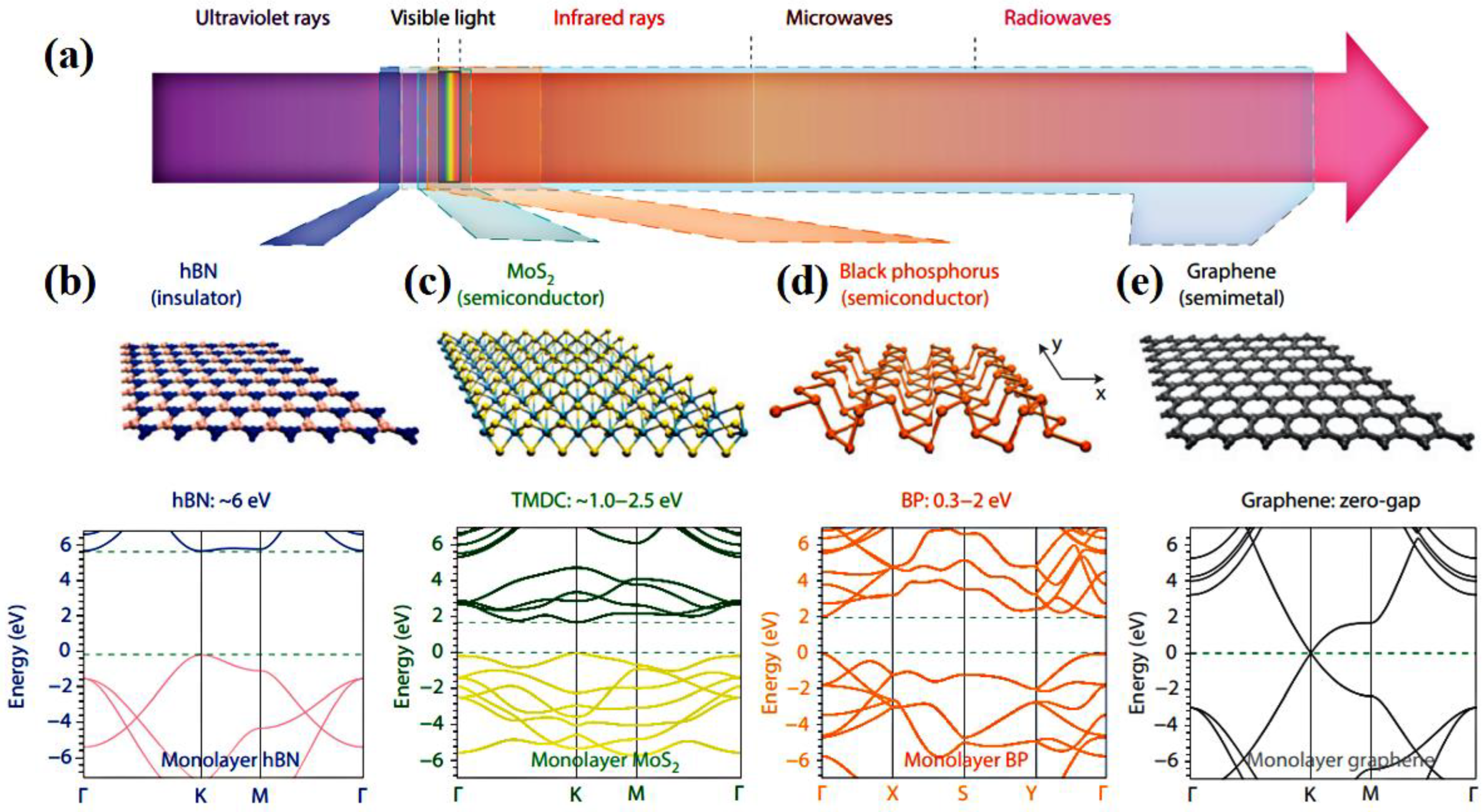
4. Two-Dimensional Material

In order to meet the application requirements of ultra-fast all-optical devices, it is necessary to combine new two-dimensional materials with strong nonlinearity. Two-dimensional (2D) materials exhibit a variety of electronic properties, from insulating hexagonal boron nitride and semiconducting transition metal dichalcogenides (TMDs, such as molybdenum disulfide) to semi-metallic graphene, as shown in Figure 1 [50]. The successful preparation of two-dimensional materials has completely released the huge potential of two-dimensional materials in the research field of all-optical devices. In recent years, 2D nanomaterials have been favored and sought after by researchers due to their unique structural characteristics and novel physical properties. Additionally, a large number of graphene-like structures have been predicted theoretically or synthesized experimentally, such as hexagonal nitride sheds, black phosphorus, transition metal-sulfur compounds, and germanene, etc. Currently, these two-dimensional materials form a particularly complete class of low-dimensional nanomaterial systems, with a wealth of properties and functional attributes to meet the needs of almost all research areas. Based on the characteristics of the layered structure of two-dimensional materials, different two-dimensional materials can form heterogeneous structures, which is extremely important for the realization of various all-optical optoelectronic devices.
The dimensionality of a material not only defines its atomic composition, but also determines, to a great extent, the properties of the material itself. Among them, the most famous material in the field of two-dimensional material technology is carbon-based material. The discovery of and research on carbon materials have promoted the progress of modern science and technology. After the early research boom of 0D fullerenes (C60) [51] and 1D single-walled carbon nanotubes [52], Geim and Novoselov et al. successfully exfoliated 2D graphene monolayers in 2004, for which they were awarded the 2010 Nobel Prize in Physics [53]. It is this hexagonal monolayer of sp2 hybridized carbon atoms that has particularly striking mechanical and electronic properties, such as a linear dispersion relation in its energy band at the K-high symmetry point in the Brillouin zone. The special energy band structure has led to many novel physical phenomena, such as the anomalous quantum Hall effect. In addition, it has opened up a whole new field of research in “Fermi-Dirac” physics. Not only that, graphene has a high transparency of 97.7% [54], has excellent mechanical properties [55], and is also an excellent conductor of electricity and heat [56,57]. Currently, graphitic materials have been successfully applied to build light-transmitting conductors, thermal interface materials, and potential barrier transistors, etc. [58]. In addition, the density of the states of graphene is near the Dirac point, and the Fermi energy level can change significantly with the carrier density shift. Thus, four-wave mixing can be enhanced by a slow light photonic crystal waveguide that is coated with a single layer of graphene. The energy gap in the patterned nanoribbons can be tuned by a proper selection of the bandwidth of the preparation, which shows the flexibility of graphene in all-optical switching [59]. Overall, the discovery of graphene can be said to have truly opened a new chapter in the study of two-dimensional materials. The great success of graphene has also encouraged researchers to actively search for other two-dimensional materials with novel physical properties. Many theoretically proposed two-dimensional monolayers have also been synthesized, including the derivatives of graphene, such as black phosphorus, transition metal carbides, and hexagonal nitrides [60,61].
Unlike graphene, the two-dimensional hexagonal boron nitride (hBN) monolayer structure is a wide-band insulator material [62]. Single-layer hBN nanosheets can be considered graphene-like materials, equivalent to graphene in which half of the carbon atoms are replaced by nitrogen atoms and the other half by boron atoms; moreover, they are white in color, such that they are often called white graphene. Compared to graphene—which possesses excellent electrical conductivity—hexagonal boron nitride is a wide band gap insulator material, which has especially good thermal and chemical conductivity, as well as neutron-absorption capabilities. Two-dimensional hexagonal boron nitride can also change its band gap width by introducing impurity atoms or atomic site lattice defects to obtain semiconductor properties. Secondly, the hBN monolayer structure has a near-flat-band-energy band signature throughout the Brillouin zone, while graphene has a linearly dispersive energy band near the Fermi energy level and thus forms a perfect Dirac cone, which is a zero-bandgap semimetal [61,63,64].
Two-dimensional material black phosphorus (BP), ever since it was reported by Prof. Zhang and Prof. Chen in 2014 [65], has been a hot topic of research in the field of two-dimensional materials. Black phosphorus is one of the three main isomers of phosphorus and is the most thermodynamically stable compared to the other two (i.e., red phosphorus and white phosphorus). Black phosphorus has four crystal structures, orthogonal, rhombic, simple cubic, and amorphous (which is orthogonal under atmospheric and room temperature conditions). Similar to graphite, bulk black phosphorus is a layered material consisting of layers of individual atoms superimposed by van der Waals interactions. However, unlike graphite, the atoms within the same layer within black phosphorus are not in the same plane. In addition, the phosphorus atoms in the same layer are in two planes above and below, showing a honeycomb-like folded structure. It is this folded structure that makes the crystal structure of black phosphorus asymmetric, resulting in properties that are very different from other two-dimensional materials, such as graphene, which exhibits a very pronounced anisotropy. First of all, black phosphorus has anisotropic mechanical properties, the asymmetry of which will lead to different mechanical properties in different directions. The photon–electron interaction is more pronounced when the incident light is polarized along the armchair edge direction of the BP nanosheet when compared to the zig-zag edge direction. Thus, the optical absorbance, transmittance, and reflectance properties provide a means to indicate the orientation of the BP crystal. Optical anisotropy further provides opportunities for the application of polarization-dependent linear and nonlinear optical devices, based on stripped BP nanosheet materials. Meanwhile, the photoelectric properties of BP are directly related to its layer number. BP is 1.51 eV, which can emit red light via excitation, and the band gap of the sample becomes smaller as the thickness increases.
In subsequent explorations, researchers have gradually shifted their focus to the monolayer material systems of transition metal dichalcogenides (TMDs) [63]. Compared to the traditional two-dimensional materials, two-dimensional transition metal materials are more abundant, and research on these materials accounts for half of the research field of two-dimensional materials [66]. In current research progress, two-dimensional transition metal materials generally have numerous advantages over graphene, making them very promising for applications in electronic devices, such as field-effect transistors, lithium-ion batteries, sensors, and photocatalysis, etc. [67]. The TMDs also exhibit a number of low-temperature-specific phenomena, including superconductivity, charge density waves, and Mott phase transitions. These unique properties are often retained when these materials are stripped into a single layer or a few layers. Due to the local effect, additional interesting properties can also be added [68,69]. Similar to graphene, when two-dimensional TMDs are thinned from a macroscopic bulk to a few layers or a single layer, its two-dimensional or even two-dimensional thickness exhibits particularly different physical properties from the bulk material. In contrast to the semi-metallic character of graphene, the TMDs show more potential for all-optical switching research due to their rich band gap variety. Therefore, TMDs are expected to surpass graphene and open up completely new research opportunities for inorganic two-dimensional materials.
In addition, the TMDs obtained by inserting carbon elements into the lattice of metallic materials are a diverse group of material systems with many interesting properties and promising applications. These materials usually have good metal conductivity and catalytic activity comparable to those of noble metals. Recently, the development of transition metal carbides has entered the research field of two-dimensional materials; for example, Duan et al. successfully prepared large-area, high-quality two-dimensional α-Mo2C ultrathin layer structures via the process of chemical vapor deposition (CVD) [70,71]. Moreover, this general synthetic method can be used to obtain more two-dimensional materials with unique properties. Such stable, high-quality two-dimensional crystalline materials not only provide a new material platform for research in the field of superconductivity physics, but also exhibit the characteristics required for an ideal material in the preparation of all-optical open-light devices.

5. All-Optical Switching Based on Two-Dimensional Materials

Although all-optical switching has seen significant progress in the field of plasma and photonic crystals, it is still a great challenge to achieve all the required indicators of all-optical switches. The nonlinear refractive index of traditional materials is small, and the ohmic loss of metals is still large. Additionally, it is difficult to achieve large nonlinear susceptibility and an ultra-fast response time at the same time for traditional nonlinear optical materials (as shown in Table 2), which also limits the application of optical third-order nonlinear materials in all-optical switches. In recent years, two-dimensional (2D) materials, represented by graphene, have been especially investigated in the field of new photonic devices (including photodetectors, optical modulators, optical absorbers, fiber lasers, etc.). Through numerous photonic studies, these materials have gradually developed into emerging candidate materials with the ability to move the current research from the nanometer scale to the two-dimensional scale. Two-dimensional materials can be tuned from insulator to metal based on their layer thickness band gap, which can be used in the application of broadband photonic devices. Two-dimensional materials similar to graphene, such as topological insulators (Bi2Se3, Bi2Te3, and Sb2Te3) and transition metal bihalogenated hydrocarbons (MoS2, WS2, WSe2, etc.), are widely studied.

5.1. Graphene

Graphene plasma provides a distinct and outstanding platform for nonlinear all-optical switching due to its high nonlinear electrical conductivity and tight optical constraints. Graphene is widely applied in optical devices, such as fiber lasers, broadband modulators, polarizers, and optical switching, etc., because of its high optical nonlinearity and wide-wavelength-range non-dispersive nonlinear optical response.
Melinda et al. first demonstrated lithographically patterned graphene ribbon structures in 2007 and found that the energy gap was closely related to the ribbon width [59]. However, in order to facilitate the peak performance of classical nonlinear devices, based on the strong deterministic interaction between single photons in single-photon nonlinear optics, Gulans et al. proved that this field confinement causes the deterministic interaction between two plasma polaritons (i.e., photons) on the picosecond time scale, as shown in Figure 2a [72]. This also shows that the single photon switch and the nonclassical light can be realized through this interaction. Without optimized phase matching, Gullans achieved a 17 nm bandwidth and −23 dB conversion efficiency. At the same time, M. Takahashi et al. proposed an optical switch controlled by a saturable absorption of graphene that was vertically inserted or loaded on the waveguide, as shown in Figure 2b [73]. The saturated absorption of graphene-inserted fiber and graphene-loaded waveguides show that the measured absorption modulation depth can meet the switching requirements experimentally. The optical saturable absorption of single-layer graphene that was vertically inserted between optical fibers and covered on ion-exchanged waveguides was measured for picosecond switching applications. In the proposed switching, the complete switching was realized by controlling the amplitude of signal light through the structure of two cascaded Mach–Zehnder interferometers. In order to control the amplitude of signal light, M. Takahashi et al. used saturated absorption in graphene. When switching, the modulation depth of the amplitude is required to be 2.414, and the corresponding intensity is 7.65 dB. In the graphene-loaded waveguide with a length of 7 mm, the modulation absorption depth of more than 10 dB was obtained experimentally. To achieve the switching and modulation of optical interactions with deeply sub-wavelength films, Shraddha et al. reported experimental observations of the all-optical modulation of light in a graphene film [74]. However, conventionally synthesized graphene relies on high-temperature and vacuum devices, which can present detrimental transfer steps that degrade the quality of graphene, thereby affecting the efficiency of nonlinear optical operations and lacking a customized pattern with a minimal footprint, as well as lacking a convenient fabrication process. Kelvin J. A. Ooi et al. demonstrated the laser-assisted direct in situ synthesis of multilayer graphene on a side-polished fiber plane under ambient conditions. Four-wave mixing (FWM) with grown graphene is used to elucidate ultrafast all-optical switching near 1550 nm to confirm nonlinear response improvements. It was demonstrated that impressive switching performances can be obtained at sub-MW/cm2 optical pump intensities with phase extinction modulations of graphene plasma waveguides [75]. In addition, the large surface-induced nonlinear enhancement caused by the tight confinement effect can potentially make the propagating plasma pump power drop to the pW range.
Further, Debnath et al. used laser irradiation in ambient conditions to synthesize multilayer graphene directly along the polished surface of a D-shaped fiber, as shown in Figure 2c [76]. They conducted ultrafast all-optical switching experiments on grown graphene at nearly 1550 nm by using the four-wave mixing (FWM) technique. They confirmed that 58.5% of the improvement in the nonlinear response came from graphene. Mehrdad Hoseini et al. achieved all-optical switching using nonlinear transport variations of the Fano resonance of a two-dimensional photonic crystal (PhC), as shown in Figure 2d. The light intensity enhancement due to Fano resonance and focus was added together to provide greater refractive index variation at the prescribed pump intensity. With a modulation depth of 90%, this reduces the threshold input intensity of the pump for conversion to ~MW/cm2. In addition, they investigated the transient state of the structure, and an optical bistable-based all-optical switch was proposed to achieve a bistable switch with a modulation depth of 50% and a switching time of about 180 fs [77]. Xiang et al. designed the light path of an all-optical switch using spatial cross-phase modulation. The results showed that the control beam can modulate the phase change in the signal light (532 nm) to achieve the on/off function [81]. This predicts that the SXPM-based ultra-sensitive switching device may provide new ideas for all-optical switching. In 2020, Masaaki et al. proposed an ultrafast all-optical switch using graphene-loaded deep-subwavelength plasmonic waveguides (30 × 20 nm2) with a switching energy of 35 fJ and a switching time of 260 fs, as shown in Figure 2e [78]. In the same year, Chu et al. investigated an all-optical phase shifter and switching for a Michelson interferometer (MI) graphene-decorated side-polished twin-core fiber (TCF), as shown in Figure 2f. An optical switching extinction ratio of 7 dB was obtained with a rise (fall) time of 55.8 ms (15.5 ms) [79]. In 2022, Popkova et al. used Bloch surface waves (BSWs) to enhance graphene–light interactions in order to achieve all-optical switching, whereby the magnitude of the reflection change reaches 0.3% at the fluence of 40 µJ cm−2 [82]. In 2023, Taghizadeh et al. investigated the effect of terahertz fields on the optical response of Landau quantized graphene monolayers and discussed the possibility of achieving ultrafast all-optical switching using terahertz field strength in the near infrared, as shown in Figure 2g [80].
In recent years, all-optical switches based on graphene and Mach–Zehnder interferometers have been widely studied. In 2019, Hao et al. proposed and experimentally demonstrated an all-optical switch based on a graphene-coated fiber Mach–Zehnder interferometer (MZI) (as shown in Figure 3a) with rise and fall times of 30 ms and 50 ms, respectively [83]. In the same year, Armaghani et al. also proposed an all-optical graphene switch based on the MZI, as shown in Figure 3b, where the switch operation can be accomplished by generating a 180-ohm phase difference between the two arms of the graphene MZI [84]. In 2021, Qiu et al. proposed and experimentally demonstrated a graphene-on-silicon nitride (Si3N4) all-optical switching based on an MZI (as shown in Figure 3c), with rise and fall time constants of 571 ns and 1.29 μs, respectively [85]. Recently, Jiang et al. proposed a graphene-buried balanced MZI structure, as shown in Figure 3d, for a low-power all-optical switch with an actual pump power absorbed by the graphene-activated switch of around 2.2 mW; the rise and fall times of the switch were 1.0 and 2.7 ms, respectively [86]. Table 3 summarizes the rise time, fall time, and switching energy of graphene based all-optical switching with different structures.

5.2. Black Phosphorus

Black Phosphorus (BP) has anisotropic nonlinear optical responses and varies with film thickness, which is quite different from other typical two-dimensional layered materials (such as graphene and transition metal dihalides). The most promising feature, thus far, of BP may be that it fills a gap in the 2D family [87,88]. Firstly, the band gap of BP is layer-dependent and covers 0.3 to 2 eV [89]. Due to its relatively strong out-of-plane quantum confinement, its bandgap-tuning range is much larger than that of other two-dimensional materials. This tunable bandgap property offers multiple advantages, with the large tuning range leading to the flexibility required in electronic or photonic applications. Next, BP transistors offer a compromise between carrier mobility and the switching ratio. Mobility and the switching ratio are the simplest metrics to characterize transistor performance. BP is now attracting a great deal of research interest. Normally, BP is a layered orthorhombic crystal with phosphorus atoms arranged in a puckered honeycomb lattice, where in a separate layer each phosphorus atom is bound to three neighboring atoms via sp3-hybridized orbitals, which is unlike the sp2-hybridized carbon atoms in graphene. In the base plane, the folding of the lattice leads to two unequal directions: the x-direction (i.e., the armchair edge) and the y-direction (i.e., the zig-zag edge).
In 2015, Li et al. generated ultrafast (i.e., a pulse duration down to 786 fs at mode locking) and large energy (Q-switched pulses up to >18 nj) pulses in a fiber laser in the ~1.5 μm NIR communication band based on the nonlinear optical properties of BP [90]. Similarly, the Sotor research group successfully obtained an ultrashort pulse with a bandwidth of 10.2 nm and a duration of 272 fs in the 1550 nm communication band using a BP-based SA [91]. All of these properties make it possible to achieve nonlinear and ultrafast all-optical applications, based on BP.
In 2016, Markus et al. designed a SiO2/black phosphorus/SiO2 heterostructure, as shown in Figure 4a, to achieve ultra-fast measures of BP at the nanoscale and to achieve switchable interface polaritons [92]. Where the surface phonon mode of the SiO2 layer hybridizes with the mode of the BP, it can then be activated by photo-induced inter-band excitation. In the Reststrahlen band of SiO2, the hybrid interface polariton has surface-phonon-like properties. In addition, it also possesses a well-defined frequency and momentum, as well as an excellent coherence. The results show that the surface mode activates in 50 fs and disappears in 5 ps with the recombination of electron-hole pairs in BP. Debnath’s group not only performed ultrafast all-optical switching experiments on grown graphene at nearly 1550 nm using the four-wave mixing (FWM) technique, as shown in Figure 4b, but also exploited the evanescent field interaction between propagating light and BP to achieve FWM [93]. They performed FWM-based wavelength conversion experiments on modulated signals in the frequency range up to 20 GHz by using a BP-based nonlinear optical device consisting of a side polished fiber or a D-shape that was deposited with BP.
The refractive index of black phosphorus is affected by high-power laser light, which is also known as the optical Kerr effect. This phenomenon enables all-optical exchange in all-optical network components. To evaluate the applicability of metal-ion-doped layer-less BP in all-optical signal processing under a nonlinear Kerr effect, a deposited sample placed onto a microfiber with a swift field interaction scheme of transmitted light and BP was used by Zheng et al. [94]. The basic operating principle and experimental setup of the Kerr switch are shown in Figure 4c. This BP-clad microfiber device can be used both as an optical Kerr switch with an extinction ratio of up to 26 dB and an operation range of more than 18 nm and an FWM-based wavelength converter with a maximum conversion efficiency of −59.15 dB. The results show that, thanks to the high nonlinear optical index and protection of several layers of BP that were doped with metal ions, the new nonlinear optical device can be used as a broadband all-optical processing device with high stability and durability, which may constitute the first prototype of BP-based optical Kerr exchange devices. In 2018, Wang et al. demonstrated, for the first time, experimentally that the sub-band structure of ultrathin black phosphorus (BP) nanosheets is caused by strong many-body effects and unique quasi-one-dimensional band dispersions. The photoexcitation processes of two different sets of BP nanosheets were demonstrated through careful analysis of photoluminescence spectra and femtosecond time-resolved transient absorption spectra. The BP nanosheets based on the energy band structure exhibit a significant optical switching effect during the generation of photocatalytic reactive oxygen species (ROS) [97]. Wang et al. demonstrated an optical Kerr switch with an extinction ratio of 20 dB with BP quantum dots deposited on the microfiber as shown in Figure 4d. The conversion efficiency of this wavelength converter in the RF band is about −40 dB [95]. In 2021, Yin et al. performed all-optical modulation experiments in a cavity of black-phosphorus-functionalized microfiber coil resonators (MCR). The resonance wavelength and extinction ratio responses to the incident pump power were ~0.033 nm mW−1 and ~0.180 dBm mW−1, respectively, with an average rise/fall time of ~9.58/8.53 ms. The device can be applied to all-optical modulators, optical switches, or tunable optical filters [96].
Table 4 summarizes the rise time, fall time, and extinction ratio of BP based all-optical switching with different structures. In summary, BP is still in its beginning, although it has recently attracted much research attention and has seen great progress. From a practical point of view, fundamental and technical issues are raised. These issues pose great challenges, as well as chances, for upcoming research in BP-based optics and photonics.

5.3. Transition Metal Dichalcogenide (TMDs)

Two-dimensional transition metal dichalcogenides (TMDs), which are denoted by the formula MX2 (where M denotes a transition metal element and X denotes a chalcogen, such as S, Se, or Te), are considered highly anticipated candidates for the next generation of electronics and photonics, with three advantages [98,99,100,101,102,103,104,105,106,107]: firstly, the weak van der Waals interactions and the lack of surface dangling bonds make the construction of heterostructures easy, thus eliminating the strict thermal and lattice matching requirements [107,108]. Secondly, the coupling of broken inversion symmetry and spin orbit in certain single-layer TMDs provides us with a new platform for studying valley electronics and fabricating spintronic devices [64,107,109,110,111]. Thirdly, certain TMDs (e.g., 2H MoS2, 2H WSe2) exhibit indirect–direct bandgaps as the number of layers is reduced to a single layer, which can stimulate various optoelectronic applications, such as photodetectors, photovoltaic devices, and light-emitting devices [112,113,114,115,116].
Unlike graphene, certain members of the TMD family are true semiconductors with a significant band gap. In particular, molybdenum and tungsten-based dihalides exhibit optical forbidden bands in the 1–2 eV range and are suitable for near-infrared absorption and emissions. Although these materials, interestingly, have an indirect band gap in the bulk and layer-less form, they have become direct gap semiconductors with strong photoluminescence at the monolayer level [112,117]. TMDs have been shown to have direct energy gaps in the near infrared to the visible spectral region, and thereby, a new window has been opened for photonics and optoelectronics. TMDs normally show resonant absorption in visible light, enabling pulsed fiber lasers in the visible region. Symmetry breaking in the TMDs leads to finite second-order optical nonlinearities. The d-electrons in layered TMDs can give rise to a variety of physical properties. Furthermore, the photoluminescence increases with decreasing coating thickness. When using two different laser power densities, a broad-range switch between the exciton and trion of the monolayer WS2 can be reversibly achieved, thus resulting in a continuous modulation of its photon absorption [118]. Seyler et al. reported a mechanism for electrically controlling second-order optical nonlinearities in a monolayer WSe2, thereby demonstrating that monolayer TMD field-effect transistors represent a new class of an electrically tunable nonlinear optical device [119]. Wu et al. demonstrated a fiber optic all-optical phase shifter, as shown in Figure 5c. It uses a layer-less two-dimensional material, such as tungsten disulfide (WS2), which is deposited on a tapered fiber. The WS2 absorbs the injected 980 nm pump light (control light) and generates heat. A maximum phase shift of 6.1π is achieved near 1550 nm due to the thermo-optical effect, which changes the refractive index of the WS2 and the tapered fiber. The device has a loss of 3.7 dB. In addition, it also has an all-optical switch with an extinction ratio of 15 dB and a rise time of 7.3 ms, which was obtained by constructing a single-arm MZI with a WS2 phase shifter [120]. This all-fiber, low-cost, and compact optical phase shifter and switch demonstrates the potential of two-dimensional transition metal dihalide compounds for all-optical signal processing devices. In addition, the nonlinear refractive index and third-order nonlinear magnetization of SnS were characterized, for the first time, by Wu et al. In addition, its powder-related nonlinear refractive index was also experimentally verified. On this basis, a new type of nonlinear all-optical switch was proposed as shown in Figure 5a. The results show that the phase change in the signal light (633 nm) can be controlled by another control light (532 nm), thus realizing the on/off mode of the all-optical switch [121]. In 2022, Xu et al. experimentally designed MoTe2 quantum dots-based all-optical switching as shown in Figure 5g in order to manipulate light (λ = 457 nm) against signal light (λ = 532 nm) using the spatial cross-phase modulation (SXPM) method [122].
The most studied material in TMDs, MoS2, is a novel two-dimensional nanomaterial with broadband high optical gain and fast optical switching. As such, it is promising to be the next generation of optical devices. Yin et al. made the first phototransistor based on a mechanically exfoliated monolayer MoS2, as shown in Figure 5e. Furthermore, the observed switching duration of the current rise (from OFF to ON) or the decay (from ON to OFF) process was only around 50 ms [125]. Tsai et al. reported, for the first time, on a new-layered MoS2 as Schottkymetal-semiconductor-metal photodetectors (MSM PDs) that are capable of broadband photodetection from visible to UV wavelengths at operating temperatures, in harsh conditions, of up to 200 °C. At a 10 V bias, photogain up to 13.3 leads to ultrahigh responsivity and detectivity for MoS2 up to 0.57 A/W and ~1010 cm Hz1/2/W, which was previously not obtainable in pristine graphene and MoS2-based PDs. Moreover, MoS2 MSM PDs show a very fast and stable optical response with a rise time of around 70 μs and a fall time of approximately 110 μs, as shown in Figure 5d. Although the thickness of several layers of MoS2 is only 1.9 nm, their light absorption in the visible region is as high as 10% [124]. In 2014, Zhang et al. investigated the nonlinear optical properties of MoS2 nanosheets from the visible to the near-infrared band using the hydrothermal exfoliation method, as shown in Figure 5b. The laser experiments showed that the mode-locker, based on MoS2 with few layers, can generate stable mode-locked laser pulses with a central wavelength of 1054.3 nm, as well as a 3 dB spectral bandwidth of 2.7 nm and a pulse duration of 800 ps [123]. In 2017, Yogesh et al. demonstrated that sharp Fano resonances in molybdenum disulfide-coated metamaterials, consisting of asymmetric split ring resonator arrays, have ultrasensitive active switching and modulation, thus allowing for ultrafast switching of Fano resonances on a 100 ps time scale, as shown in Figure 5f [126]. Table 5 summarizes the rise time, fall time, and extinction ratio of TMDs based on all-optical switching with different structures.

5.4. Layered Material Heterostructures

Two-dimensional materials have attracted much attention from researchers due to their unique optical band gap structure, extremely strong light–matter interactions, and large specific surface areas. Graphene, hexagonal boron nitride (h-BN), and certain other transition metal dihalides (TMDs) have emerged as promising new materials. They are composed of strong covalent bonds transversely, which provide great in-plane stability. The recent development of vapor-phase growth techniques for two-dimensional materials has further paved the way for directly synthesizing vertical and lateral heterojunctions. Each layer in a two-dimensional layered material consists of a covalently bonded, dangling-bond-free lattice and is weakly bonded to neighboring layers via van der Waals interactions. This makes it possible to separate, mix, and match highly different atomic layers in order to create a wide range of van der Waals heterostructures without the limitations of lattice matching and processing compatibility [110]. Integrating two-dimensional materials with a variety of nanoscale materials can create a wide range of van der Waals heterogeneous structures with previously impossible functions. The exfoliation and restacking of various 2D materials opens up a flexible path for the design and creation of a new generation of optical switches. As a result, the heterojunctions of 2D-layered materials have become a hot new topic, opening up new areas of material science and device applications [127,128,129]. For example, it has been shown that laminates of graphene and hexagonal boron nitride (hBN), molybdenum disulfide (MoS2), or tungsten disulfide (WS2) can run tunneling transistors [130,131]. This is in addition to phenomena, such as Coulomb drag resistance [132] and the fractional quantum Hall effect [133], which can also be observed.
Raman scattering photo luminescence and absorption spectra can be used to characterize interlayer interactions. In addition, exciton dynamics can be studied using transient absorption spectra. This allows electronic and optical properties to be elucidated non-destructively, accurately, and efficiently, thereby optimizing the fabrication of these stacked junctions and improving the design of new structures [134,135,136,137,138,139,140,141,142,143]. Ferrari et al. first demonstrated that the profile of the 2D Raman peak evolves with an increasing number of graphene layers. Lui et al. found a significant difference in the Raman 2D peak shape between ABA and ABC stacked tri- and quad-layer graphene [144]. Cong and Zhang et al. also found that the M-band profile at ~1750 cm−1 and the peak position in the G-band were very sensitive to the stacking order of the few layers of graphene [145,146].
Isolated atomically layered two-dimensional materials can be combined into connections with precisely defined configurations, such as lateral junctions and vertical junctions [147,148,149]. Early studies have shown that van der Waals stacks of 2D materials work especially well and greatly enrich the optoelectronic applications of 2D materials.
The weak van der Waals inter-layer force is able to isolate two-dimensional monolayers and restack them into arbitrary stacking heterojunctions without regard to atomic commensurability. Two-dimensional heterostructures are van der Waals-bonded heterostructures, which offer greater flexibility than conventional covalently bonded heterostructures. Without the constraint of atomically precise commensurability, it is possible to create high-quality semiconductor heterointerfaces. Two-dimensional heterostructures that have been studied include graphene-BP, TMD-TMD, TMD-graphene, and TMD-hBN combinations [127,128,150,151]. Heterogeneous structures involving TMD have strong light–matter interactions and unique optical properties that are essential for all-optical modulation applications [152]. It has been demonstrated that graphene-semiconducting TMD-graphene heterostructures exhibit strong photo–matter interactions, which can lead to large photon absorption and photocurrent production [153]. Another experiment shows that hole transfer from the MoS2 layer to the WS2 layer is very fast, within 50 fs of photoexcitation. This opens up the possibility of new types of two-dimensional light trapping devices [140]. Optoelectronic devices based on an MoS2/WSe2 vertical heterojunction have also recently been demonstrated, as shown in Figure 6b [154]. In 2016, large nonlinear refraction (n2 = 0.2 × 10⁻⁷ cm2/W) and ultrafast dynamic relaxation times (intraband relaxation time τ 1 = 270   ±   20   fs ; inter-band relaxation time τ 2 = 3 . 6   ±   0 . 2   ps ) of the graphene–Bi2Te3 heterostructure were reported [155]. Recently, an anisotropic infrared plasmonic broadband absorber based on graphene–BP multilayers was proposed by Cai et al.
The vertical junctions of two-dimensional atomic-layered materials can be achieved via simple mechanical transfer without lattice mismatch [157]. However, lateral heterojunctions cannot be achieved through mechanical transfer, and lateral epitaxial growth is the best method for preparing atomic-layered lateral heterojunctions. Unlike vertical Van-der-Waals-stacked heterojunctions, lattice mismatch is a key issue for seamless transverse 2D junctions. In addition, lattice mismatches between MoS2 and WS2, MoSe2 and WSe2, MoS2 and MoSe2, WS2 and WSe2, and graphene and hBN are relatively small (<4%) [156,158,159,160,161,162,163]. The Van der Waals heterostructures can be achieved via transfer or direct epitaxial growth by using these two-dimensional layered materials. Xu et al. systematically investigated photocurrents in monolayer–bilayer graphene homojunctions [164]. Howell and colleagues studied photocurrent generation in both monolayer and multilayer MoS2 film interfaces [165]. Graphene–boron nitride(BN)-based two-dimensional lateral heterostructures have been reported [156,165,166,167]. It has also been successfully demonstrated that the lateral heteroepitaxial junctions of two-dimensional layered semiconductors can be grown using the lateral heteroepitaxial approach. Graphene and hBN have a tight lattice match (1.7%); therefore, a near-perfect transverse graphene hBN junction can be achieved. In addition, Levendorf and colleagues reported the versatile, scalable regeneration of hBN monolayers, which can be performed from the edges of pre-patterned graphene monolayers [162]. Liu et al. proposed that growing graphene in a flat hBN atomic layer can form a transverse graphene–hBN heterostructure, as shown in Figure 5c [156]. Duan et al. prepared the transverse heterostructures of MoS2, MoSe2 and WS2, and WSe2 through the in situ modulation of the vapor-phase reactants. Moreover, Raman and photoluminescence mapping studies showed that the resulting heterostructured domains exhibit clear structural and optical modulations [71].

6. Summary and Outlook

In recent years, profound achievements have been made in the field of all-optical switches in terms of nonlinear materials, device structures, triggering methods, advanced performance indicators, and chip integration compatibility. Materials with excellent third-order nonlinear optical response properties are an important basis for improving the performance index of all-optical switches. Two-dimensional materials are represented by graphene, black phosphorus, and TMDs. The emergence of new materials with good third-order optical nonlinearity provides an important impetus for the improvement of all-optical switches. This not only provides a way to build ultrafast nonlinear media, overcoming the inherent material limitations that constrain the development of integrated photonic devices, but also provides a lab-on-chip platform for the study of novel physical effects.
The integration of 2D materials into photonic platforms is currently limited. Although 2D-material all-optical switches are not yet well established, they may be better suited for on-chip integration by using simple, inexpensive, and scalable post-processing techniques. Within the rich family of 2D materials, there are many more candidates to explore. In addition, the bottlenecks with respect to their use for large-scale applications may soon be replaced by recent breakthroughs in wafer-scale synthesis methods and manufacturing processes [168,169]. In the last few years, certain breakthroughs in switching times and energy consumption have been made in integrated optical switches, aided by, for example, two-dimensional materials. However, it is still hard to further reduce the energy consumption to the attojoule-level, which is necessary for large-scale photonic-integrated circuits in the future. This requires a detailed, systematic, and in-depth exploration of the mechanisms that enhance light–matter interactions, i.e., the mechanisms and methods that control the interaction of multiple physical fields (i.e., light, heat, and electric fields) within the medium. The ultra-fast switching of attojoule-level energy consumption can be achieved based on emerging nanomaterials, as well as the properties of plasma, nanophotonics, and hybrid integration. More efforts must be made in this area to further improve performance.

Author Contributions

Conceptualization, formal analysis, and writing—original draft, J.X., Y.P., L.J. and S.Q.; writing—original draft preparation, J.X. and Y.P.; data curation and funding acquisition, Y.P., L.J. and S.Q.; project administration and supervision, L.J. and S.Q.; data analysis, writing—review, and editing, J.X., Y.P., L.J. and S.Q. All authors have read and agreed to the published version of the manuscript.

Funding

This work was supported by the National Natural Science Foundation of China (Grant Nos.11774088, 11704119), Scientific Research Fund of Hunan Provincial Education Department (Grant No. 21B0048), the Hunan Provincial Natural Science Foundation of China (Grant Nos. 2021JJ30149), and the Changsha Natural Science Foundation (Grant No. kq2202236).

Data Availability Statement

The datasets used and/or analyzed during the current study are available from the corresponding author upon reasonable request.

Conflicts of Interest

The authors declare no conflict of interest.

References

  1. Chai, Z.; Hu, X.; Wang, F.; Niu, X.; Xie, J.; Gong, Q. Ultrafast All-Optical Switching. Adv. Opt. Mater. 2017, 5, 1600665. [Google Scholar] [CrossRef]
  2. Nozaki, K.; Tanabe, T.; Shinya, A.; Matsuo, S.; Sato, T.; Taniyama, H.; Notomi, M. Sub-femtojoule all-optical switching using a photonic-crystal nanocavity. Nat. Photonics 2010, 4, 477–483. [Google Scholar] [CrossRef]
  3. Altug, H.; Englund, D.; Vučković, J. Ultrafast photonic crystal nanocavity laser. Nat. Phys. 2006, 2, 484–488. [Google Scholar] [CrossRef]
  4. Venkatesan, T.; Lemaire, P.J.; Wilkens, B.; Soto, L.; Gossard, A.C.; Wiegmann, W.; Jewell, J.L.; Gibbs, H.M.; Tarng, S.S. All-optical data switching in an optical-fiber link using a GaAs optical bistable device. Opt. Lett. 1984, 9, 297–299. [Google Scholar] [CrossRef] [PubMed]
  5. Van, V.; Ibrahim, T.; Ritter, K.; Absil, P.; Johnson, F.; Grover, R.; Goldhar, J.; Ho, P.-T. All-optical nonlinear switching in GaAs-AlGaAs microring resonators. IEEE Photonics Tech. L. 2002, 14, 74–76. [Google Scholar] [CrossRef]
  6. Almeida, V.R.; Barrios, C.A.; Panepucci, R.R.; Lipson, M. All-optical control of light on a silicon chip. Nature 2004, 431, 1081–1084. [Google Scholar] [CrossRef]
  7. Koos, C.; Vorreau, P.; Vallaitis, T.; Dumon, P.; Bogaerts, W.; Baets, R.; Esembeson, B.; Biaggio, I.; Michinobu, T.; Diederich, F. All-optical high-speed signal processing with silicon–organic hybrid slot waveguides. Nat. Photonics 2009, 3, 216. [Google Scholar] [CrossRef]
  8. Nie, W. Optical Nonlinearity:Phenomena, applications, and materials. Adv. Mater. 1993, 5, 520–545. [Google Scholar] [CrossRef]
  9. Leuthold, J.; Koos, C.; Freude, W. Nonlinear silicon photonics. Nat. Photonics 2010, 4, 535–544. [Google Scholar] [CrossRef]
  10. Dobbelaere, P.D.; Falta, K.; Gloeckner, S.; Patra, S. Digital MEMS for optical switching. IEEE Commun. Mag. 2002, 40, 88–95. [Google Scholar] [CrossRef]
  11. Ikeda, K.; Saperstein, R.E.; Alic, N.; Fainman, Y. Thermal and Kerr nonlinear properties of plasma-deposited silicon nitride/silicon dioxide waveguides. Opt. Express 2008, 16, 12987–12994. [Google Scholar] [CrossRef] [PubMed]
  12. Lu, H.; Liu, X.; Wang, L.; Gong, Y.; Mao, D. Ultrafast all-optical switching in nanoplasmonic waveguide with Kerr nonlinear resonator. Opt. Express 2011, 19, 2910–2915. [Google Scholar] [CrossRef] [PubMed]
  13. Waldow, M.; Plötzing, T.; Gottheil, M.; Först, M.; Bolten, J.; Wahlbrink, T.; Kurz, H. 25ps all-optical switching in oxygen implanted silicon-on-insulator microring resonator. Opt. Express 2008, 16, 7693–7702. [Google Scholar] [CrossRef] [PubMed]
  14. Li, N.; Xu, J.; Song, G.; Zhu, C.; Xie, S.; Yang, Y.; Zubairy, M.S.; Zhu, S.-Y. Nonlinear all-optical switch based on a white-light cavity. Phys. Rev. A 2016, 93, 043819. [Google Scholar] [CrossRef]
  15. Haché, A.; Bourgeois, M. Ultrafast all-optical switching in a silicon-based photonic crystal. Appl. Phys. Lett. 2000, 77, 4089–4091. [Google Scholar] [CrossRef]
  16. Almeida, V.R.; Lipson, M. Optical bistability on a silicon chip. Opt. Lett. 2004, 29, 2387–2389. [Google Scholar] [CrossRef]
  17. Li, S.; Cai, X. High-contrast all optical bistable switching in coupled nonlinear photonic crystal microcavities. Appl. Phys. Lett. 2010, 96, 131114. [Google Scholar] [CrossRef]
  18. Scalora, M.; Dowling, J.P.; Bowden, C.M.; Bloemer, M.J. Optical Limiting and Switching of Ultrashort Pulses in Nonlinear Photonic Band Gap Materials. Phys. Rev. Lett. 1994, 73, 1368–1371. [Google Scholar] [CrossRef]
  19. Kim, C.; May-Arrioja, D.A.; LiKamWa, P.; Newman, P.; Pamulapati, J. Ultrafast all-optical multiple quantum well integrated optic switch. Electron. Lett. 2000, 36, 1929–1930. [Google Scholar] [CrossRef]
  20. Delgado-Pinar, M.; Zalvidea, D.; Díez, A.; Pérez-Millán, P.; Andrés, M.V. Q-switching of an all-fiber laser by acousto-optic modulation of a fiber Bragg grating. Opt. Express 2006, 14, 1106–1112. [Google Scholar] [CrossRef]
  21. Ren, M.; Jia, B.; Ou, J.-Y.; Plum, E.; Zhang, J.; MacDonald, K.F.; Nikolaenko, A.E.; Xu, J.; Gu, M.; Zheludev, N.I. Nanostructured Plasmonic Medium for Terahertz Bandwidth All-Optical Switching. Adv. Mater. 2011, 23, 5540–5544. [Google Scholar] [CrossRef] [PubMed]
  22. Tran, P. Optical limiting and switching of short pulses by use of a nonlinear photonic bandgap structure with a defect. J. Opt. Soc. Am. B 1997, 14, 2589–2595. [Google Scholar] [CrossRef]
  23. Fan, S. Sharp asymmetric line shapes in side-coupled waveguide-cavity systems. Appl. Phys. Lett. 2002, 80, 908–910. [Google Scholar] [CrossRef]
  24. Yanik, M.F.; Fan, S.; Soljačić, M. High-contrast all-optical bistable switching in photonic crystal microcavities. Appl. Phys. Lett. 2003, 83, 2739–2741. [Google Scholar] [CrossRef]
  25. Wada, O. Femtosecond all-optical devices for ultrafast communication and signal processing. New J. Phys. 2004, 6, 183. [Google Scholar] [CrossRef]
  26. Pasquazi, A.; Stivala, S.; Assanto, G.; Amendola, V.; Meneghetti, M.; Cucini, M.; Comoretto, D. In situ tuning of a photonic band gap with laser pulses. Appl. Phys. Lett. 2008, 93, 091111. [Google Scholar] [CrossRef]
  27. Dani, K.M.; Ku, Z.; Upadhya, P.C.; Prasankumar, R.P.; Brueck, S.R.J.; Taylor, A.J. Subpicosecond Optical Switching with a Negative Index Metamaterial. Nano Lett. 2009, 9, 3565–3569. [Google Scholar] [CrossRef]
  28. Boyd, R. Nonlinear Optics; Academic Pres Inc.: Boston, MA, USA, 1992. [Google Scholar]
  29. Slusher, R.E. Nonlinear Photonic Crystals; Springer Science & Business Media: Berlin, Germany, 2003; Volume 10. [Google Scholar]
  30. Sakoda, K. Optical Properties of Photonic Crystals; Springer Science & Business Media: Berlin, Germany, 2004; Volume 80. [Google Scholar]
  31. Euser, T.G.; Molenaar, A.J.; Fleming, J.G.; Gralak, B.; Polman, A.; Vos, W.L. All-optical octave-broad ultrafast switching of Si woodpile photonic band gap crystals. Phys. Rev. B 2008, 77, 115214. [Google Scholar] [CrossRef]
  32. Yablonovitch, E. Photonic crystals: What’s in a name? Opt. Photonics News 2007, 18, 12–13. [Google Scholar]
  33. Tanabe, T.; Notomi, M.; Mitsugi, S.; Shinya, A.; Kuramochi, E. All-optical switches on a silicon chip realized using photonic crystal nanocavities. Appl. Phys. Lett. 2005, 87, 151112. [Google Scholar] [CrossRef]
  34. Nau, D.; Bertram, R.; Buse, K.; Zentgraf, T.; Kuhl, J.; Tikhodeev, S.; Gippius, N.; Giessen, H. Optical switching in metallic photonic crystal slabs with photoaddressable polymers. Appl. Phys. B 2006, 82, 543–547. [Google Scholar] [CrossRef]
  35. Zhao, Y.; Qian, C.; Qiu, K.; Gao, Y.; Xu, X. Ultrafast optical switching using photonic molecules in photonic crystal waveguides. Opt. Express 2015, 23, 9211–9220. [Google Scholar] [CrossRef] [PubMed]
  36. Enoch, S.; Quidant, R.; Badenes, G. Optical sensing based on plasmon coupling in nanoparticle arrays. Opt. Express 2004, 12, 3422–3427. [Google Scholar] [CrossRef]
  37. Drachev, V.P.; Chettiar, U.K.; Kildishev, A.V.; Yuan, H.-K.; Cai, W.; Shalaev, V.M. The Ag dielectric function in plasmonic metamaterials. Opt. Express 2008, 16, 1186–1195. [Google Scholar] [CrossRef] [PubMed]
  38. Krasavin, A.; Zayats, A. All-optical active components for dielectric-loaded plasmonic waveguides. Opt. Commun. 2010, 283, 1581–1584. [Google Scholar] [CrossRef]
  39. Barnes, W.L.; Dereux, A.; Ebbesen, T.W. Surface plasmon subwavelength optics. Nature 2003, 424, 824–830. [Google Scholar] [CrossRef]
  40. Gramotnev, D.K.; Bozhevolnyi, S.I. Plasmonics beyond the diffraction limit. Nat. Photonics 2010, 4, 83–91. [Google Scholar] [CrossRef]
  41. Porto, J.; Martin-Moreno, L.; Garcia-Vidal, F. Optical bistability in subwavelength slit apertures containing nonlinear media. Phys. Rev. B 2004, 70, 081402. [Google Scholar] [CrossRef]
  42. Smolyaninov, I.I. Quantum fluctuations of the refractive index near the interface between a metal and a nonlinear dielectric. Phys. Rev. Lett. 2005, 94, 057403. [Google Scholar] [CrossRef]
  43. Min, C.; Wang, P.; Chen, C.; Deng, Y.; Lu, Y.; Ming, H.; Ning, T.; Zhou, Y.; Yang, G. All-optical switching in subwavelength metallic grating structure containing nonlinear optical materials. Opt. Lett. 2008, 33, 869–871. [Google Scholar] [CrossRef]
  44. Min, C.; Veronis, G. Absorption switches in metal-dielectric-metal plasmonic waveguides. Opt. Express 2009, 17, 10757–10766. [Google Scholar] [CrossRef] [PubMed]
  45. Zhong, Z.-J.; Xu, Y.; Lan, S.; Dai, Q.-F.; Wu, L.-J. Sharp and asymmetric transmission response in metal-dielectric-metal plasmonic waveguides containing Kerr nonlinear media. Opt. Express 2010, 18, 79–86. [Google Scholar] [CrossRef] [PubMed]
  46. Chai, Z.; Hu, X.; Zhu, Y.; Sun, S.; Yang, H.; Gong, Q. Ultracompact Chip-Integrated Electromagnetically Induced Transparency in a Single Plasmonic Composite Nanocavity. Adv. Opt. Mater. 2014, 2, 320–325. [Google Scholar] [CrossRef]
  47. Nazarathy, M.; Zalevsky, Z.; Rudnitsky, A.; Larom, B.; Nevet, A.; Orenstein, M.; Fischer, B. All-optical linear reconfigurable logic with nonlinear phase erasure. J. Opt. Soc. Am. A 2009, 26, A21–A39. [Google Scholar] [CrossRef]
  48. Alexe-Ionescu, A.-L.; Ionescu, A.T.; Barna, E.S.; Barna, V.; Scaramuzza, N. Fast electro-optic switching in nematic liquid crystals. Appl. Phys. Lett. 2003, 84, 40–42. [Google Scholar] [CrossRef]
  49. Shcherbakov, M.R.; Vabishchevich, P.P.; Shorokhov, A.S.; Chong, K.E.; Choi, D.-Y.; Staude, I.; Miroshnichenko, A.E.; Neshev, D.N.; Fedyanin, A.A.; Kivshar, Y.S. Ultrafast All-Optical Switching with Magnetic Resonances in Nonlinear Dielectric Nanostructures. Nano Lett. 2015, 15, 6985–6990. [Google Scholar] [CrossRef]
  50. Xia, F.; Wang, H.; Xiao, D.; Dubey, M.; Ramasubramaniam, A. Two-dimensional material nanophotonics. Nat. Photonics 2014, 8, 899–907. [Google Scholar] [CrossRef]
  51. Kroto, H.; Heath, J.; O’brien, S.; Curl, R.; Smalley, R. This Week’s Citation Classic®. Nature 1985, 318, 162–163. [Google Scholar] [CrossRef]
  52. Iijima, S. Helical microtubules of graphitic carbon. Nature 1991, 354, 56–58. [Google Scholar] [CrossRef]
  53. Novoselov, K.S.; Geim, A.K.; Morozov, S.V.; Jiang, D.; Zhang, Y.; Dubonos, S.V.; Grigorieva, I.V.; Firsov, A.A. Electric field effect in atomically thin carbon films. Science 2004, 306, 666–669. [Google Scholar] [CrossRef]
  54. Nair, R.R.; Blake, P.; Grigorenko, A.N.; Novoselov, K.S.; Booth, T.J.; Stauber, T.; Peres, N.M.; Geim, A.K. Fine structure constant defines visual transparency of graphene. Science 2008, 320, 1308. [Google Scholar] [CrossRef] [PubMed]
  55. Lee, C.; Wei, X.; Kysar, J.W.; Hone, J. Measurement of the elastic properties and intrinsic strength of monolayer graphene. Science 2008, 321, 385–388. [Google Scholar] [CrossRef] [PubMed]
  56. Balandin, A.A. Thermal properties of graphene and nanostructured carbon materials. Nat. Mater. 2011, 10, 569–581. [Google Scholar] [CrossRef]
  57. Morozov, S.; Novoselov, K.; Katsnelson, M.; Schedin, F.; Elias, D.; Jaszczak, J.A.; Geim, A. Giant intrinsic carrier mobilities in graphene and its bilayer. Phys. Rev. Lett. 2008, 100, 016602. [Google Scholar] [CrossRef] [PubMed]
  58. Butler, S.Z.; Hollen, S.M.; Cao, L.; Cui, Y.; Gupta, J.A.; Gutiérrez, H.R.; Heinz, T.F.; Hong, S.S.; Huang, J.; Goldberger, J.E.; et al. Progress, Challenges, and Opportunities in Two-Dimensional Materials Beyond Graphene. ACS Nano 2013, 7, 2898–2926. [Google Scholar] [CrossRef] [PubMed]
  59. Han, M.Y.; Özyilmaz, B.; Zhang, Y.; Kim, P. Energy Band-Gap Engineering of Graphene Nanoribbons. Phys. Rev. Lett. 2007, 98, 206805. [Google Scholar] [CrossRef] [PubMed]
  60. Kim, K.K.; Hsu, A.; Jia, X.; Kim, S.M.; Shi, Y.; Hofmann, M.; Nezich, D.; Rodriguez-Nieva, J.F.; Dresselhaus, M.; Palacios, T. Synthesis of monolayer hexagonal boron nitride on Cu foil using chemical vapor deposition. Nano Lett. 2012, 12, 161–166. [Google Scholar] [CrossRef]
  61. Zhi, C.; Bando, Y.; Tang, C.; Kuwahara, H.; Golberg, D. Large-scale fabrication of boron nitride nanosheets and their utilization in polymeric composites with improved thermal and mechanical properties. Adv. Mater. 2009, 21, 2889–2893. [Google Scholar] [CrossRef]
  62. Giovannetti, G.; Khomyakov, P.A.; Brocks, G.; Kelly, P.J.; Van Den Brink, J. Substrate-induced band gap in graphene on hexagonal boron nitride: Ab initio density functional calculations. Phys. Rev. B 2007, 76, 073103. [Google Scholar] [CrossRef]
  63. Han, J.H.; Lee, S.; Cheon, J. Synthesis and structural transformations of colloidal 2D layered metal chalcogenide nanocrystals. Chem. Soc. Rev. 2013, 42, 2581–2591. [Google Scholar] [CrossRef]
  64. Chhowalla, M.; Shin, H.S.; Eda, G.; Li, L.-J.; Loh, K.P.; Zhang, H. The chemistry of two-dimensional layered transition metal dichalcogenide nanosheets. Nat. Chem. 2013, 5, 263. [Google Scholar] [CrossRef] [PubMed]
  65. Li, L.; Yu, Y.; Ye, G.J.; Ge, Q.; Ou, X.; Wu, H.; Feng, D.; Chen, X.H.; Zhang, Y. Black phosphorus field-effect transistors. Nat. Nanotechnol. 2014, 9, 372–377. [Google Scholar] [CrossRef] [PubMed]
  66. Choi, W.; Choudhary, N.; Han, G.H.; Park, J.; Akinwande, D.; Lee, Y.H. Recent development of two-dimensional transition metal dichalcogenides and their applications. Mater. Today 2017, 20, 116–130. [Google Scholar] [CrossRef]
  67. Wang, Q.H.; Kalantar-Zadeh, K.; Kis, A.; Coleman, J.N.; Strano, M.S. Electronics and optoelectronics of two-dimensional transition metal dichalcogenides. Nat. Nanotechnol. 2012, 7, 699. [Google Scholar] [CrossRef] [PubMed]
  68. Zeng, H.; Dai, J.; Yao, W.; Xiao, D.; Cui, X. Valley polarization in MoS2 monolayers by optical pumping. Nat. Nanotechnol. 2012, 7, 490. [Google Scholar] [CrossRef]
  69. Cao, T.; Wang, G.; Han, W.; Ye, H.; Zhu, C.; Shi, J.; Niu, Q.; Tan, P.; Wang, E.; Liu, B.; et al. Valleyselective circular dichroism of monolayer molybdenum disulphide. Nat. Commun. 2012, 3, 887. [Google Scholar] [CrossRef]
  70. Guimarães, M.H.; Gao, H.; Han, Y.; Kang, K.; Xie, S.; Kim, C.-J.; Muller, D.A.; Ralph, D.C.; Park, J. Atomically thin ohmic edge contacts between two-dimensional materials. ACS Nano 2016, 10, 6392–6399. [Google Scholar] [CrossRef]
  71. Duan, X.; Wang, C.; Shaw, J.C.; Cheng, R.; Chen, Y.; Li, H.; Wu, X.; Tang, Y.; Zhang, Q.; Pan, A. Lateral epitaxial growth of two-dimensional layered semiconductor heterojunctions. Nat. Nanotechnol. 2014, 9, 1024. [Google Scholar] [CrossRef]
  72. Gullans, M.; Chang, D.E.; Koppens, F.H.L.; de Abajo, F.J.G.; Lukin, M.D. Single-Photon Nonlinear Optics with Graphene Plasmons. Phys. Rev. Lett. 2013, 111, 247401. [Google Scholar] [CrossRef]
  73. Takahashi, M.; Ueda, W.; Goto, N.; Yanagiya, S. Saturable Absorption by Vertically Inserted or Overlaid Monolayer Graphene in Optical Waveguide for All-Optical Switching Circuit. IEEE Photonics J. 2013, 5, 6602109. [Google Scholar] [CrossRef]
  74. Rao, S.M.; Heitz, J.J.F.; Roger, T.; Westerberg, N.; Faccio, D. Coherent control of light interaction with graphene. Opt. Lett. 2014, 39, 5345–5347. [Google Scholar] [CrossRef]
  75. Ooi, K.J.A.; Cheng, J.L.; Sipe, J.E.; Ang, L.K.; Tan, D.T.H. Ultrafast, broadband, and configurable midinfrared all-optical switching in nonlinear graphene plasmonic waveguides. APL Photonics 2016, 1, 046101. [Google Scholar] [CrossRef]
  76. Debnath, P.C.; Uddin, S.; Song, Y.-W. Ultrafast All-Optical Switching Incorporatingin SituGraphene Grown along an Optical Fiber by the Evanescent Field of a Laser. ACS Photonics 2017, 5, 445–455. [Google Scholar] [CrossRef]
  77. Hoseini, M.; Malekmohammad, M. All-optical high performance graphene-photonic crystal switch. Opt. Commun. 2017, 383, 159–164. [Google Scholar] [CrossRef]
  78. Ono, M.; Hata, M.; Tsunekawa, M.; Nozaki, K.; Sumikura, H.; Chiba, H.; Notomi, M. Ultrafast and energy-efficient all-optical switching with graphene-loaded deep-subwavelength plasmonic waveguides. Nat. Photonics 2020, 14, 37–43. [Google Scholar] [CrossRef]
  79. Chu, R.; Guan, C.; Bo, Y.; Liu, J.; Shi, J.; Yang, J.; Ye, P.; Li, P.; Yang, J.; Yuan, L. Graphene decorated twin-core fiber Michelson interferometer for all-optical phase shifter and switch. Opt. Lett. 2020, 45, 177–180. [Google Scholar] [CrossRef]
  80. Taghizadeh, M.; Bozorgzadeh, F.; Bordbar, G.H. All-optical diffraction and ultrafast switching in a terahertz-driven quantized graphene system. Opt. Laser Technol. 2023, 159, 108969. [Google Scholar] [CrossRef]
  81. Shan, Y.; Tang, J.; Wu, L.; Lu, S.; Dai, X.; Xiang, Y. Spatial self-phase modulation and all-optical switching of graphene oxide dispersions. J. Alloys Compd. 2019, 771, 900–904. [Google Scholar] [CrossRef]
  82. Popkova, A.A.; Chezhegov, A.A.; Rybin, M.G.; Soboleva, I.V.; Obraztsova, E.D.; Bessonov, V.O.; Fedyanin, A.A. Bloch Surface Wave-Assisted Ultrafast All-Optical Switching in Graphene. Adv. Opt. Mater. 2022, 10, 2101937. [Google Scholar] [CrossRef]
  83. Hao, T.; Chang, Z.; Chiang, K.S. Externally pumped low-loss graphene-based fiber Mach-Zehnder all-optical switches with mW switching powers. Opt. Express 2019, 27, 4216–4225. [Google Scholar] [CrossRef]
  84. Armaghani, S.; Khani, S.; Danaie, M. Design of all-optical graphene switches based on a Mach-Zehnder interferometer employing optical Kerr effect. Superlattices Microstruct. 2019, 135, 106244. [Google Scholar] [CrossRef]
  85. Qiu, C.; Zhang, C.; Zeng, H.; Guo, T. High-Performance Graphene-on-Silicon Nitride All-Optical Switch Based on a Mach–Zehnder Interfometer. J. Light. Technol. 2021, 39, 2099–2105. [Google Scholar] [CrossRef]
  86. Jiang, L.; Huang, Q.; Chiang, K.S. Low-power all-optical switch based on a graphene-buried polymer waveguide Mach-Zehnder interferometer. Opt. Express 2022, 30, 6786–6797. [Google Scholar] [CrossRef]
  87. Ling, X.; Wang, H.; Huang, S.; Xia, F.; Dresselhaus, M.S. The renaissance of black phosphorus. Proc. Natl. Acad. Sci. USA 2015, 112, 4523. [Google Scholar] [CrossRef]
  88. Castellanos-Gomez, A. Black Phosphorus: Narrow Gap, Wide Applications. J. Phys. Chem. Lett. 2015, 6, 4280–4291. [Google Scholar] [CrossRef]
  89. Tran, V.; Soklaski, R.; Liang, Y.; Yang, L. Layer-controlled band gap and anisotropic excitons in few-layer black phosphorus. Phys. Rev. B 2014, 89, 235319. [Google Scholar] [CrossRef]
  90. Li, D.; Jussila, H.; Karvonen, L.; Ye, G.; Lipsanen, H.; Chen, X.; Sun, Z. Polarization and Thickness Dependent Absorption Properties of Black Phosphorus: New Saturable Absorber for Ultrafast Pulse Generation. Sci. Rep. 2015, 5, 15899. [Google Scholar] [CrossRef]
  91. Sotor, J.; Sobon, G.; Macherzynski, W.; Paletko, P.; Abramski, K.M. Black phosphorus saturable absorber for ultrashort pulse generation. Appl. Phys. Lett. 2015, 107, 051108. [Google Scholar] [CrossRef]
  92. Huber, M.A.; Mooshammer, F.; Plankl, M.; Viti, L.; Sandner, F.; Kastner, L.Z.; Frank, T.; Fabian, J.; Vitiello, M.S.; Cocker, T.L.; et al. Femtosecond photo-switching of interface polaritons in black phosphorus heterostructures. Nat. Nanotechnol. 2017, 12, 207–211. [Google Scholar] [CrossRef] [PubMed]
  93. Uddin, S.; Debnath, P.C.; Park, K.; Song, Y.-W. Nonlinear Black Phosphorus for Ultrafast Optical Switching. Sci. Rep. 2017, 7, 43371. [Google Scholar] [CrossRef]
  94. Zheng, J.; Yang, Z.; Si, C.; Liang, Z.; Chen, X.; Cao, R.; Guo, Z.; Wang, K.; Zhang, Y.; Ji, J.; et al. Black Phosphorus Based All-Optical-Signal-Processing: Toward High Performances and Enhanced Stability. ACS Photonics 2017, 4, 1466–1476. [Google Scholar] [CrossRef]
  95. Wang, K.; Chen, Y.; Zheng, J.; Ge, Y.; Ji, J.; Song, Y.; Zhang, H. Black phosphorus quantum dot based all-optical signal processing: Ultrafast optical switching and wavelength converting. Nanotechnology 2019, 30, 415202. [Google Scholar] [CrossRef]
  96. Yin, Y.; Li, S.; Ren, J.; Du, Y.; Farrell, G.; Brambilla, G.; Wang, P. All-optical modulation in Black Phosphorus functionalized microfibre coil resonator. Meas. Sci. Technol. 2020, 32, 015202. [Google Scholar] [CrossRef]
  97. Wang, H.; Jiang, S.; Shao, W.; Zhang, X.; Chen, S.; Sun, X.; Zhang, Q.; Luo, Y.; Xie, Y. Optically Switchable Photocatalysis in Ultrathin Black Phosphorus Nanosheets. J. Am. Chem. Soc. 2018, 140, 3474–3480. [Google Scholar] [CrossRef] [PubMed]
  98. Shim, J.; Jang, S.W.; Lim, J.-H.; Kim, H.; Kang, D.-H.; Kim, K.-H.; Seo, S.; Heo, K.; Shin, C.; Yu, H.-Y.; et al. Polarity control in a single transition metal dichalcogenide (TMD) transistor for homogeneous complementary logic circuits. Nanoscale 2019, 11, 12871–12877. [Google Scholar] [CrossRef] [PubMed]
  99. Tan, C.; Cao, X.; Wu, X.-J.; He, Q.; Yang, J.; Zhang, X.; Chen, J.; Zhao, W.; Han, S.; Nam, G.-H.; et al. Recent Advances in Ultrathin Two-Dimensional Nanomaterials. Chem. Rev. 2017, 117, 6225–6331. [Google Scholar] [CrossRef]
  100. Hu, Z.; Wu, Z.; Han, C.; He, J.; Ni, Z.; Chen, W. Two-dimensional transition metal dichalcogenides: Interface and defect engineering. Chem. Soc. Rev. 2018, 47, 3100–3128. [Google Scholar] [CrossRef]
  101. Long, M.; Wang, P.; Fang, H.; Hu, W. Progress, Challenges, and Opportunities for 2D Material Based Photodetectors. Adv. Funct. Mater. 2019, 29, 1803807. [Google Scholar] [CrossRef]
  102. Wang, G.; Li, L.; Fan, W.; Wang, R.; Zhou, S.; Lü, J.-T.; Gan, L.; Zhai, T. Interlayer Coupling Induced Infrared Response in WS2/MoS2 Heterostructures Enhanced by Surface Plasmon Resonance. Adv. Funct. Mater. 2018, 28, 1800339. [Google Scholar] [CrossRef]
  103. Li, L.; Wang, W.; Chai, Y.; Li, H.; Tian, M.; Zhai, T. Few-Layered PtS2 Phototransistor on h-BN with High Gain. Adv. Funct. Mater. 2017, 27, 1701011. [Google Scholar] [CrossRef]
  104. Li, L.; Han, W.; Pi, L.; Niu, P.; Han, J.; Wang, C.; Su, B.; Li, H.; Xiong, J.; Bando, Y.; et al. Emerging in-plane anisotropic two-dimensional materials. InfoMat 2019, 1, 54–73. [Google Scholar] [CrossRef]
  105. Wang, R.; Zhou, F.; Lv, L.; Zhou, S.; Yu, Y.; Zhuge, F.; Li, H.; Gan, L.; Zhai, T. Modulation of the Anisotropic Electronic Properties in ReS2 via Ferroelectric Film. CCS Chem. 2019, 1, 268–277. [Google Scholar]
  106. You, H.; Zhuo, Z.; Lu, X.; Liu, Y.; Guo, Y.; Wang, W.; Yang, H.; Wu, X.; Li, H.; Zhai, T. 1T′-MoTe2-Based On-Chip Electrocatalytic Microdevice: A Platform to Unravel Oxidation-Dependent Electrocatalysis. CCS Chem. 2019, 1, 396–406. [Google Scholar] [CrossRef]
  107. Zhang, W.; Wang, Q.; Chen, Y.; Wang, Z.; Wee, A.T.S. Van der Waals stacked 2D layered materials for optoelectronics. 2D Mater. 2016, 3, 022001. [Google Scholar] [CrossRef]
  108. Liu, Y.; Weiss, N.O.; Duan, X.; Cheng, H.-C.; Huang, Y.; Duan, X. Van der Waals heterostructures and devices. Nat. Rev. Mater. 2016, 1, 16042. [Google Scholar] [CrossRef]
  109. Mak, K.F.; He, K.; Shan, J.; Heinz, T.F. Control of valley polarization in monolayer MoS2 by optical helicity. Nat. Nanotechnol. 2012, 7, 494–498. [Google Scholar] [CrossRef] [PubMed]
  110. Xiao, D.; Liu, G.-B.; Feng, W.; Xu, X.; Yao, W. Coupled Spin and Valley Physics in Monolayers of MoS2 and Other Group-VI Dichalcogenides. Phys. Rev. Lett. 2012, 108, 196802. [Google Scholar] [CrossRef]
  111. Splendiani, A.; Sun, L.; Zhang, Y.; Li, T.; Kim, J.; Chim, C.-Y.; Galli, G.; Wang, F. Emerging Photoluminescence in Monolayer MoS2. Nano Lett. 2010, 10, 1271–1275. [Google Scholar] [CrossRef]
  112. Huang, X.; Zeng, Z.; Zhang, H. Metal dichalcogenide nanosheets: Preparation, properties and applications. Chem. Soc. Rev. 2013, 42, 1934–1946. [Google Scholar] [CrossRef]
  113. Mak, K.F.; Lee, C.; Hone, J.; Shan, J.; Heinz, T.F. Atomically Thin MoS2: A New Direct-Gap Semiconductor. Phys. Rev. Lett. 2010, 105, 136805. [Google Scholar] [CrossRef]
  114. Eda, G.; Yamaguchi, H.; Voiry, D.; Fujita, T.; Chen, M.; Chhowalla, M. Photoluminescence from Chemically Exfoliated MoS2. Nano Lett. 2011, 11, 5111–5116. [Google Scholar] [CrossRef] [PubMed]
  115. Tongay, S.; Zhou, J.; Ataca, C.; Lo, K.; Matthews, T.S.; Li, J.; Grossman, J.C.; Wu, J. Thermally Driven Crossover from Indirect toward Direct Bandgap in 2D Semiconductors: MoSe2 versus MoS2. Nano Lett. 2012, 12, 5576–5580. [Google Scholar] [CrossRef] [PubMed]
  116. Zhao, W.; Ghorannevis, Z.; Chu, L.; Toh, M.; Kloc, C.; Tan, P.-H.; Eda, G. Evolution of Electronic Structure in Atomically Thin Sheets of WS2 and WSe2. ACS Nano 2013, 7, 791–797. [Google Scholar] [CrossRef] [PubMed]
  117. Chowdhury, T.; Erick, C.S.; Thomas, J.K. Progress and prospects in transition-metal dichalcogenide research beyond 2D. Chem. Rev. 2020, 120, 12563–12591. [Google Scholar] [CrossRef]
  118. Yang, C.; Gao, Y.; Qin, C.; Liang, X.; Han, S.; Zhang, G.; Chen, R.; Hu, J.; Xiao, L.; Jia, S. All-Optical Reversible Manipulation of Exciton and Trion Emissions in Monolayer WS2. Nanomaterials 2020, 10, 23. [Google Scholar] [CrossRef]
  119. Seyler, K.L.; Schaibley, J.R.; Gong, P.; Rivera, P.; Jones, A.M.; Wu, S.; Yan, J.; Mandrus, D.G.; Yao, W.; Xu, X. Electrical control of second-harmonic generation in a WSe2 monolayer transistor. Nat. Nanotechnol. 2015, 10, 407–411. [Google Scholar] [CrossRef]
  120. Wu, K.; Guo, C.; Wang, H.; Zhang, X.; Wang, J.; Chen, J. All-optical phase shifter and switch near 1550 nm using tungsten disulfide (WS2) deposited tapered fiber. Opt. Express 2017, 25, 17639–17649. [Google Scholar] [CrossRef]
  121. Wu, L.; Xie, Z.; Lu, L.; Zhao, J.; Wang, Y.; Jiang, X.; Ge, Y.; Zhang, F.; Lu, S.; Guo, Z.; et al. Few-Layer Tin Sulfide: A Promising Black-Phosphorus-Analogue 2D Material with Exceptionally Large Nonlinear Optical Response, High Stability, and Applications in All-Optical Switching and Wavelength Conversion. Adv. Opt. Mater. 2018, 6, 1700985. [Google Scholar] [CrossRef]
  122. Xu, H.; Lin, Z.; Dai, X. MoTe2 quantum dots-based all-optical switching. Opt. Commun. 2022, 506, 127573. [Google Scholar] [CrossRef]
  123. Zhang, H.; Lu, S.B.; Zheng, J.; Du, J.; Wen, S.C.; Tang, D.Y.; Loh, K.P. Molybdenum disulfide (MoS2) as a broadband saturable absorber for ultra-fast photonics. Opt. Express 2014, 22, 7249–7260. [Google Scholar] [CrossRef]
  124. Tsai, D.-S.; Liu, K.-K.; Lien, D.-H.; Tsai, M.-L.; Kang, C.-F.; Lin, C.-A.; Li, L.-J.; He, J.-H. Few-Layer MoS2 with High Broadband Photogain and Fast Optical Switching for Use in Harsh Environments. ACS Nano 2013, 7, 3905–3911. [Google Scholar] [CrossRef] [PubMed]
  125. Yin, Z.; Li, H.; Li, H.; Jiang, L.; Shi, Y.; Sun, Y.; Lu, G.; Zhang, Q.; Chen, X.; Zhang, H. Single-Layer MoS2 Phototransistors. ACS Nano 2012, 6, 74–80. [Google Scholar] [CrossRef]
  126. Srivastava, Y.K.; Chaturvedi, A.; Manjappa, M.; Kumar, A.; Dayal, G.; Kloc, C.; Singh, R. MoS2 for Ultrafast All-Optical Switching and Modulation of THz Fano Metaphotonic Devices. Adv. Opt. Mater. 2017, 5, 1700762. [Google Scholar] [CrossRef]
  127. Geim, A.K.; Grigorieva, I.V. Van der Waals heterostructures. Nature 2013, 499, 419–425. [Google Scholar] [CrossRef] [PubMed]
  128. Wang, H.; Liu, F.; Fu, W.; Fang, Z.; Zhou, W.; Liu, Z. Two-dimensional heterostructures: Fabrication, characterization, and application. Nanoscale 2014, 6, 12250–12272. [Google Scholar] [CrossRef]
  129. Buscema, M.; Island, J.O.; Groenendijk, D.J.; Blanter, S.I.; Steele, G.A.; van der Zant, H.S.J.; Castellanos-Gomez, A. Photocurrent generation with two-dimensional van der Waals semiconductors. Chem. Soc. Rev. 2015, 44, 3691–3718. [Google Scholar] [CrossRef]
  130. Britnell, L.; Gorbachev, R.V.; Jalil, R.; Belle, B.D.; Schedin, F.; Mishchenko, A.; Georgiou, T.; Katsnelson, M.I.; Eaves, L.; Morozov, S.V.; et al. Field-Effect Tunneling Transistor Based on Vertical Graphene Heterostructures. Science 2012, 335, 947. [Google Scholar] [CrossRef]
  131. Georgiou, T.; Jalil, R.; Belle, B.D.; Britnell, L.; Gorbachev, R.V.; Morozov, S.V.; Kim, Y.-J.; Gholinia, A.; Haigh, S.J.; Makarovsky, O.; et al. Vertical field-effect transistor based on graphene–WS2 heterostructures for flexible and transparent electronics. Nat. Nanotechnol. 2013, 8, 100–103. [Google Scholar] [CrossRef]
  132. Gorbachev, R.V.; Geim, A.K.; Katsnelson, M.I.; Novoselov, K.S.; Tudorovskiy, T.; Grigorieva, I.V.; MacDonald, A.H.; Morozov, S.V.; Watanabe, K.; Taniguchi, T.; et al. Strong Coulomb drag and broken symmetry in double-layer graphene. Nat. Phys. 2012, 8, 896–901. [Google Scholar] [CrossRef]
  133. Dean, C.R.; Young, A.F.; Cadden-Zimansky, P.; Wang, L.; Ren, H.; Watanabe, K.; Taniguchi, T.; Kim, P.; Hone, J.; Shepard, K.L. Multicomponent fractional quantum Hall effect in graphene. Nat. Phys. 2011, 7, 693–696. [Google Scholar] [CrossRef]
  134. Rivera, P.; Schaibley, J.R.; Jones, A.M.; Ross, J.S.; Wu, S.; Aivazian, G.; Klement, P.; Seyler, K.; Clark, G.; Ghimire, N.J.; et al. Observation of long-lived interlayer excitons in monolayer MoSe2–WSe2 heterostructures. Nat. Commun. 2015, 6, 6242. [Google Scholar] [CrossRef] [PubMed]
  135. Chiu, M.-H.; Li, M.-Y.; Zhang, W.; Hsu, W.-T.; Chang, W.-H.; Terrones, M.; Terrones, H.; Li, L.-J. Spectroscopic Signatures for Interlayer Coupling in MoS2–WSe2 van der Waals Stacking. ACS Nano 2014, 8, 9649–9656. [Google Scholar] [CrossRef] [PubMed]
  136. Fang, H.; Battaglia, C.; Carraro, C.; Nemsak, S.; Ozdol, B.; Kang Jeong, S.; Bechtel Hans, A.; Desai Sujay, B.; Kronast, F.; Unal Ahmet, A.; et al. Strong interlayer coupling in van der Waals heterostructures built from single-layer chalcogenides. Proc. Natl. Acad. Sci. USA 2014, 111, 6198–6202. [Google Scholar] [CrossRef] [PubMed]
  137. Tongay, S.; Fan, W.; Kang, J.; Park, J.; Koldemir, U.; Suh, J.; Narang, D.S.; Liu, K.; Ji, J.; Li, J.; et al. Tuning Interlayer Coupling in Large-Area Heterostructures with CVD-Grown MoS2 and WS2 Monolayers. Nano Lett. 2014, 14, 3185–3190. [Google Scholar] [CrossRef] [PubMed]
  138. Ceballos, F.; Bellus, M.Z.; Chiu, H.-Y.; Zhao, H. Ultrafast Charge Separation and Indirect Exciton Formation in a MoS2–MoSe2 van der Waals Heterostructure. ACS Nano 2014, 8, 12717–12724. [Google Scholar] [CrossRef]
  139. Hong, X.; Kim, J.; Shi, S.-F.; Zhang, Y.; Jin, C.; Sun, Y.; Tongay, S.; Wu, J.; Zhang, Y.; Wang, F. Ultrafast charge transfer in atomically thin MoS2/WS2 heterostructures. Nat. Nanotechnol. 2014, 9, 682–686. [Google Scholar] [CrossRef]
  140. Zhou, K.-G.; Withers, F.; Cao, Y.; Hu, S.; Yu, G.; Casiraghi, C. Raman Modes of MoS2 Used as Fingerprint of van der Waals Interactions in 2-D Crystal-Based Heterostructures. ACS Nano 2014, 8, 9914–9924. [Google Scholar] [CrossRef]
  141. Wu, M.; Zeng, X.C. Intrinsic Ferroelasticity and/or Multiferroicity in Two-Dimensional Phosphorene and Phosphorene Analogues. Nano Lett. 2016, 16, 3236–3241. [Google Scholar] [CrossRef]
  142. Castellanos-Gomez, A.; van der Zant, H.S.J.; Steele, G.A. Folded MoS2 layers with reduced interlayer coupling. Nano Res. 2014, 7, 572–578. [Google Scholar] [CrossRef]
  143. Crowne, F.J.; Amani, M.; Birdwell, A.G.; Chin, M.L.; O’Regan, T.P.; Najmaei, S.; Liu, Z.; Ajayan, P.M.; Lou, J.; Dubey, M. Blueshift of the $A$-exciton peak in folded monolayer MoS2. Phys. Rev. B 2013, 88, 235302. [Google Scholar] [CrossRef]
  144. Lui, C.H.; Li, Z.; Chen, Z.; Klimov, P.V.; Brus, L.E.; Heinz, T.F. Imaging Stacking Order in Few-Layer Graphene. Nano Lett. 2011, 11, 164–169. [Google Scholar] [CrossRef] [PubMed]
  145. Cong, C.; Yu, T.; Sato, K.; Shang, J.; Saito, R.; Dresselhaus, G.F.; Dresselhaus, M.S. Raman Characterization of ABA- and ABC-Stacked Trilayer Graphene. ACS Nano 2011, 5, 8760–8768. [Google Scholar] [CrossRef] [PubMed]
  146. Zhang, W.; Yan, J.; Chen, C.-H.; Lei, L.; Kuo, J.-L.; Shen, Z.; Li, L.-J. Molecular adsorption induces the transformation of rhombohedral- to Bernal-stacking order in trilayer graphene. Nat. Commun. 2013, 4, 2074. [Google Scholar] [CrossRef] [PubMed]
  147. Cui, X.; Lee, G.-H.; Kim, Y.D.; Arefe, G.; Huang, P.Y.; Lee, C.-H.; Chenet, D.A.; Zhang, X.; Wang, L.; Ye, F.; et al. Multi-terminal transport measurements of MoS2 using a van der Waals heterostructure device platform. Nat. Nanotechnol. 2015, 10, 534–540. [Google Scholar] [CrossRef]
  148. Kang, J.; Tongay, S.; Zhou, J.; Li, J.; Wu, J. Band offsets and heterostructures of two-dimensional semiconductors. Appl. Phys. Lett. 2013, 102, 012111. [Google Scholar] [CrossRef]
  149. Huang, S.; Ling, X.; Liang, L.; Kong, J.; Terrones, H.; Meunier, V.; Dresselhaus, M.S. Probing the Interlayer Coupling of Twisted Bilayer MoS2 Using Photoluminescence Spectroscopy. Nano Lett. 2014, 14, 5500–5508. [Google Scholar] [CrossRef]
  150. Jariwala, D.; Sangwan, V.K.; Lauhon, L.J.; Marks, T.J.; Hersam, M.C. Emerging Device Applications for Semiconducting Two-Dimensional Transition Metal Dichalcogenides. ACS Nano 2014, 8, 1102–1120. [Google Scholar] [CrossRef]
  151. Wang, H.; Yuan, H.; Sae Hong, S.; Li, Y.; Cui, Y. Physical and chemical tuning of two-dimensional transition metal dichalcogenides. Chem. Soc. Rev. 2015, 44, 2664–2680. [Google Scholar] [CrossRef]
  152. Huo, N.; Kang, J.; Wei, Z.; Li, S.-S.; Li, J.; Wei, S.-H. Novel and Enhanced Optoelectronic Performances of Multilayer MoS2–WS2 Heterostructure Transistors. Adv. Funct. Mater. 2014, 24, 7025–7031. [Google Scholar] [CrossRef]
  153. Britnell, L.; Ribeiro, R.M.; Eckmann, A.; Jalil, R.; Belle, B.D.; Mishchenko, A.; Kim, Y.J.; Gorbachev, R.V.; Georgiou, T.; Morozov, S.V.; et al. Strong Light-Matter Interactions in Heterostructures of Atomically Thin Films. Science 2013, 340, 1311. [Google Scholar] [CrossRef]
  154. Furchi, M.M.; Pospischil, A.; Libisch, F.; Burgdörfer, J.; Mueller, T. Photovoltaic Effect in an Electrically Tunable van der Waals Heterojunction. Nano Lett. 2014, 14, 4785–4791. [Google Scholar] [CrossRef] [PubMed]
  155. Wang, Y.; Mu, H.; Li, X.; Yuan, J.; Chen, J.; Xiao, S.; Bao, Q.; Gao, Y.; He, J. Observation of large nonlinear responses in a graphene-Bi2Te3 heterostructure at a telecommunication wavelength. Appl. Phys. Lett. 2016, 108, 221901. [Google Scholar] [CrossRef]
  156. Liu, Z.; Ma, L.; Shi, G.; Zhou, W.; Gong, Y.; Lei, S.; Yang, X.; Zhang, J.; Yu, J.; Hackenberg, K.P.; et al. In-plane heterostructures of graphene and hexagonal boron nitride with controlled domain sizes. Nat. Nanotechnol. 2013, 8, 119–124. [Google Scholar] [CrossRef]
  157. Huang, C.; Wu, S.; Sanchez, A.M.; Peters, J.J.P.; Beanland, R.; Ross, J.S.; Rivera, P.; Yao, W.; Cobden, D.H.; Xu, X. Lateral heterojunctions within monolayer MoSe2–WSe2 semiconductors. Nat. Mater. 2014, 13, 1096–1101. [Google Scholar] [CrossRef]
  158. Gong, Y.; Lei, S.; Ye, G.; Li, B.; He, Y.; Keyshar, K.; Zhang, X.; Wang, Q.; Lou, J.; Liu, Z.; et al. Two-Step Growth of Two-Dimensional WSe2/MoSe2 Heterostructures. Nano Lett. 2015, 15, 6135–6141. [Google Scholar] [CrossRef] [PubMed]
  159. Gong, Y.; Lin, J.; Wang, X.; Shi, G.; Lei, S.; Lin, Z.; Zou, X.; Ye, G.; Vajtai, R.; Yakobson, B.I.; et al. Vertical and in-plane heterostructures from WS2/MoS2 monolayers. Nat. Mater. 2014, 13, 1135–1142. [Google Scholar] [CrossRef]
  160. Tang, M.; Zhang, D.; Wang, D.; Deng, J.; Kong, D.; Zhang, H. Performance prediction of 2D vertically stacked MoS2-WS2 heterostructures base on first-principles theory and Pearson correlation coefficient. Appl. Surf. Sci. 2022, 596, 153498. [Google Scholar] [CrossRef]
  161. Heo, H.; Sung, J.H.; Jin, G.; Ahn, J.-H.; Kim, K.; Lee, M.-J.; Cha, S.; Choi, H.; Jo, M.-H. Rotation-Misfit-Free Heteroepitaxial Stacking and Stitching Growth of Hexagonal Transition-Metal Dichalcogenide Monolayers by Nucleation Kinetics Controls. Adv. Mater 2015, 27, 3803–3810. [Google Scholar] [CrossRef]
  162. Levendorf, M.P.; Kim, C.-J.; Brown, L.; Huang, P.Y.; Havener, R.W.; Muller, D.A.; Park, J. Graphene and boron nitride lateral heterostructures for atomically thin circuitry. Nature 2012, 488, 627–632. [Google Scholar] [CrossRef]
  163. Haigh, S.J.; Gholinia, A.; Jalil, R.; Romani, S.; Britnell, L.; Elias, D.C.; Novoselov, K.S.; Ponomarenko, L.A.; Geim, A.K.; Gorbachev, R. Cross-sectional imaging of individual layers and buried interfaces of graphene-based heterostructures and superlattices. Nat. Mater. 2012, 11, 764–767. [Google Scholar] [CrossRef]
  164. Xu, X.; Gabor, N.M.; Alden, J.S.; van der Zande, A.M.; McEuen, P.L. Photo-Thermoelectric Effect at a Graphene Interface Junction. Nano Lett. 2010, 10, 562–566. [Google Scholar] [CrossRef] [PubMed]
  165. Howell, S.L.; Jariwala, D.; Wu, C.-C.; Chen, K.-S.; Sangwan, V.K.; Kang, J.; Marks, T.J.; Hersam, M.C.; Lauhon, L.J. Investigation of Band-Offsets at Monolayer–Multilayer MoS2 Junctions by Scanning Photocurrent Microscopy. Nano Lett. 2015, 15, 2278–2284. [Google Scholar] [CrossRef] [PubMed]
  166. Liu, L.; Park, J.; Siegel David, A.; McCarty Kevin, F.; Clark Kendal, W.; Deng, W.; Basile, L.; Idrobo Juan, C.; Li, A.-P.; Gu, G. Heteroepitaxial Growth of Two-Dimensional Hexagonal Boron Nitride Templated by Graphene Edges. Science 2014, 343, 163–167. [Google Scholar] [CrossRef] [PubMed]
  167. Lu, J.; Zhang, K.; Feng Liu, X.; Zhang, H.; Chien Sum, T.; Castro Neto, A.H.; Loh, K.P. Order–disorder transition in a two-dimensional boron–carbon–nitride alloy. Nat. Commun. 2013, 4, 2681. [Google Scholar] [CrossRef]
  168. Liu, Y.; Huang, Y.; Duan, X. Van der Waals integration before and beyond two-dimensional materials. Nature 2019, 567, 323–333. [Google Scholar] [CrossRef]
  169. Bae, S.-H.; Kum, H.; Kong, W.; Kim, Y.; Choi, C.; Lee, B.; Lin, P.; Park, Y.; Kim, J. Integration of bulk materials with two-dimensional materials for physical coupling and applications. Nat. Mater. 2019, 18, 550–560. [Google Scholar] [CrossRef]
Figure 1. Examples of 2D materials covering a broad spectral range [50]. (a) Electromagnetic spectrum. (be) Are the atomic structure and the band structures of (b) hBN, (c) MoS2, (d) BP, and (e) graphene.
Coatings 13 00876 g001
Figure 2. (a) A doped graphene disk confines photons [72]. (b) Waveguide structure with an overlaid graphene sheet [73]. (c) Ultrafast all-optical switching based on FWM mixing in situ synthesized graphene [76]. (d) Nonlinear transmission variation in all-optical switching for Fano resonance in two-dimensional photonic crystals [77]. (e) Schematic diagram of an all-optical control of graphene-supported metal-insulator-metal WG and the electric field distribution of characteristic modes E 2 [78]. (f) The schematic diagram of the side-polished two-core fiber Michelson interferometer [79]. (g) The schematic diagram of laser-induced graphene-based diffraction grating [80].
Coatings 13 00876 g002
Figure 3. (a) Graphene-based fiber Mach–Zehnder all-optical switches [83]. (b) All-optical switches based on graphene and insulated metal plasma waveguides [84]. (c) Graphene-on-silicon nitride all-optical switching [85]. (d) Graphene-buried balanced Mach–Zehnder interferometer [86].
Coatings 13 00876 g003
Figure 4. (a) The SiO2/BP/SiO2 heterostructure [92]. (b) A schematic diagram of the experimental apparatus for FWM observation in a BP-deposited apparatus [93]. (c) A Kerr switch based on black phosphorus [94]. (d) The Kerr switcher in a BPQD-deposited nonlinear fiber optical device [95]. (e) The response time of black-phosphorus-functionalized microfiber coil resonators with different pump powers [96].
Coatings 13 00876 g004
Figure 5. (a) Schematic of SXPM in a few-layer SnS [121]. (b) Schematic diagram of the Z−scan experimental setup [123]. (c) Experimental setup of the all-optical phase shifter and switching, based on a WS2-tapered fiber [120]. (d) Schematic of the optical microscopic top-view image and switching characteristic of the few-layer MoS2 MSM PDs [124]. (e) Optical switching characteristics and stability of monolayer MoS2 phototransistors (in room temperature) [125]. (f) MoS2 drop casted on a terahertz asymmetric split ring resonator structure [126]. (g) MoTe2 quantum dots, based all-optical switching [122].
Coatings 13 00876 g005
Figure 6. (a) Schematic diagram of the MoS2/WS2 heterostructure [139]. (b) MoS2/WSe2 hetero−diode and current−voltage characteristics of the MoS2/WSe2 vertical heterojunction under light [154]. (c) Epitaxial growth lateral graphene−hBN heterostructures [156]. (d) Schematic diagram of the transverse epitaxial growth of WS2–WSe2 and MoS2–MoSe2 heterostructures [71].
Coatings 13 00876 g006
Table 1. Nonlinear mechanisms and corresponding switching principles.
Nonlinear MechanismsSwitching Principles
Nonlinear refractionOptical Kerr effect, self-focusing, self-defocusing, and the two-photon refraction effect
Nonlinear absorptionSaturated and reverse saturable absorption, two-photon absorption, and dichroism
Nonlinear reflectionReflection at the nonlinear interface or on the surface of two prisms containing nonlinear liquid
Nonlinear polarizationNonlinear optical rotation effect of liquid crystal and chiral materials caused by strong light
Nonlinear frequency conversionFrequency doubling, sum frequency, parametric process, four-wave mixing, stimulated Raman scattering, etc.
Nonlinear phase transitionPhoto-induced material phase transitions causes a change in the refractive index or absorption coefficient of the medium
Nonlinear gratingsSingle nonlinear grating and the grating pair are connected by nonlinear waveguides
Nonlinear couplersThe phase difference between the two arms of light are caused by a strong light incident nonlinear symmetric optical coupler
Nonlinear amplifierStrong light saturates the semiconductor optical amplifier and changes the phase of light
Nonlinear interferometerThe change in the refractive index of the interferometer material is caused by the strong light, which causes the phase difference between the two beams to be π
Table 2. The characteristic parameters of several nonlinear optical materials.
Nonlinear Materials n 2 / ( cm 2 / W ) α 0 / cm −1 τ / s Q / [ cm 3 / s · W ]
PleLiquid crystal (ferroelectric liquid crystal, etc.)10−710310−310−7
Semiconductors (GaAs, etc.)10−810410−810−4
Organic materials (PTS, etc.)10−1610−110−1210−3
Glass (Si, SiO2, etc.)10−2010−510−1410−1
Table 3. Characteristic parameters of several all optical switching based on graphene.
StructureRise TimeFall TimeSwitching EnergyReference
graphene-loaded deep-subwavelength plasmonic waveguides260 fs260 fs35 fJ[76]
graphene decorated side-polished twin-core fiber Michelson interferometer 55.8 ms15.5 ms/[77]
graphene-coated fiber Mach–Zehnder interferometer30 ms50 ms4.8 mW[83]
graphene-on-silicon nitride (Si3N4) all-optical switch based on Mach–Zehnder interferometer571 ns1.29 μs/[85]
graphene-buried balanced Mach–Zehnder interferometer1.0 ms2.7 ms2.2 mW[86]
Table 4. Characteristic parameters of several all-optical switching based on BP.
StructureRise TimeFall TimeExtinction RatioReference
SiO2/BP/SiO2 heterostructure50 fs5 ps/[92]
BP-clad microfiber device//26 dB[94]
BP quantum dots deposited on the microfiber//20 dB[96]
BP functionalized microfibre coil resonator9.58 ms8.53 ms~0.180 dBm mW−1[97]
Table 5. Characteristic parameters of several all-optical switches based on TMDs.
StructureRise TimeFall TimeExtinction RatioReference
WS2 deposited tapered fiber7.3 ms/15 dB[120]
Few-layered MoS2 as Schottky metal semiconductor metal photodetectors70 μs110 μs/[124]
phototransistor based on mechanically exfoliated monolayer MoS250 ms50 ms/[125]
Disclaimer/Publisher’s Note: The statements, opinions and data contained in all publications are solely those of the individual author(s) and contributor(s) and not of MDPI and/or the editor(s). MDPI and/or the editor(s) disclaim responsibility for any injury to people or property resulting from any ideas, methods, instructions or products referred to in the content.

