Abstract
Multi-terminal artificial synaptic devices are promising for building neural morphological networks and manufacturing neural chips. In this study, planar multi-gate InOx-based artificial synaptic transistor was demonstrated by using solution-processed AlOx as an electric double layer (EDL) dielectric with mobile hydrogen protons. The excitatory postsynaptic current (EPSC) was successfully controlled by adjusting amplitude, duration, and interval of the stimulating voltage pulses applied on the planar gates. The EPSC stimulated by multiple inputs shows the property of sublinear summation. As spatial resolution function of the artificial synaptic transistor, the EPSC depends on the presynaptic (planar gate) area and distance to the channel, nonlinearly. The paired-pulse facilitation (PPF), depending on time sequence, demonstrates the temporal resolution function of the multi-gate artificial synaptic transistor. The study shows the potential of planar multi-gate AlOx/InOx EDL transistor as multi-terminal artificial synaptic device.
1. Introduction
The traditional computers adopting Von Neumann architecture are increasingly limited by the separation of storage and computing, making it difficult to achieve lower power consumption and higher speed in information processing [1]. With the development of artificial intelligence, constructing neural systems of the human brain is the main way to solve these problems [2]. Massive parallel computing in information processing can be performed by human brain with a low consumption [3,4]. In the human brain, neurons and synapses are two basic units of the neural system [5,6,7]. Therefore, the artificial synaptic devices are required to emulate the synapses. In recent years, memristors, phase change memories, atomic switches, and other two-terminal devices have been extensively studied as artificial synapses [8,9,10,11,12]. Important synaptic learning rules, such as paired-pulse facilitation (PPF), spike-time-dependent plasticity (STDP), short-term plasticity (STP) to long-term plasticity (LTP) transition, and neural network computing have been demonstrated. However, the two-terminal devices are limited, as the learning process and signal transmission cannot be performed together [13]. Three-terminal artificial synaptic devices, such as transistors, have been proposed, which learn by the gate and transmit signals by the drain current [13,14,15,16].
Nowadays, as three-terminal devices, electric double layer transistors (EDLTs) have been intensively investigated owing to their advantages of high carrier density and low operation voltage. In EDLTs, compared with conventional oxide insulators, electrolytes are promising alternatives. By using electrolytes, positive and negative carriers can be accumulated at the channel/electrolyte interface by applying external electric field. This is commonly referred to as EDL [17]. As the thickness of EDL is ~1 nm, equal current value can be achieved with such a small gate voltage [18,19,20,21]. Interestingly, the EDLTs show transfer characteristics with anticlockwise hysteresis. The mobile protons can play the active role in Faradaic charge transfer and pseudocapacitance [22]. As the proton transport in electrolyte membranes is similar to that of neurotransmitters in biological synapses, the EDLTs have been widely considered as artificial synapses. Dai et al. reported organic synaptic EDLTS with wood-derived cellulose nanopapers dielectrics [23]. Liu et al. reported synaptic EDLTs with indium zinc oxide (IZO) channel on chitosan membranes [24]. Wang et al. reported IZO-based synaptic transistor with a SiO2 EDL dielectric [25]. Biomaterials, such as cellulose nanopaper, chitosan, and inorganic materials, such as some oxides, can act as EDL dielectrics. Various kinds of neural functions, from the excitatory postsynaptic current (EPSC) to PPF, have been demonstrated.
In the human brain, each neuron connects to thousands of others through synapses. To realize complex neural networks, multi-input artificial synaptic devices are more favorable [15]. Therefore, compared with conventional single-input artificial synaptic devices, multi-input artificial synaptic devices are expected. Fortunately, in EDL, the protons can be laterally migrated and finally accumulated at the channel/electrolyte interface by applying external electric field, and high EDL capacitance can be formed. As a result, the EDLTs can be modulated by multiple coplanar gates. Based on proton-related lateral coupling effect, a multi-gate EDLT artificial synapse can be designed for complex neural networks with high integration [26]. Qing Wan et al. first reported the artificial synaptic device based on multi-gate EDLT, and they further demonstrated its spatiotemporal information processing and synaptic mimicking properties [27,28,29]. However, there is not much research on the multi-gate artificial synaptic transistor at present.
In our previous work, the synaptic transistor based on solution-processed AlOx EDL dielectric and solution-processed InOx channel has been demonstrated with a bottom gate [30,31]. Compared with the synaptic EDLTs with ionic liquids or polymer electrolytes, the combination of inorganic solid electrolyte and metal oxide semiconductors showed good process compatibility, repeatability, and reliability. However, the multi-gate artificial synaptic transistor has not been studied yet. In this work, we demonstrated multi-gate artificial synaptic transistor with AlOx/InOx stack layer. The neural functions (EPSC, PPF, STP and LTP) and multi-dimensional information, such as time and space, were simulated. This work provides a basic device for the development of complex neural network computing.
2. Experiment Details
We prepared AlOx precursor solution by dissolving aluminum nitrate in mixed solution of ammonium hydroxide, nitric acid, and hydrogen peroxide. Similarly, we prepared InOx precursor solution by dissolving indium nitrate in deionized water. The multi-gate EDLT artificial synaptic devices were fabricated on a heavily doped silicon wafer substrate. As EDL, AlOx film was spin-coated on the substrate by using AlOx precursor solution and annealed on a hot plate at 300 °C in air for 30 min. The spin-coating process and annealing process were repeated five times. Then, the InOx channel layer was spin-coated on the AlOx layer by using InOx precursor solution and annealed on the hot plate at 230 °C in air for 2 h. The InOx channel was patterned with a width of 96 µm and a length of 24 µm by photolithography and etching. At last, the source/drain electrodes and top gates were fabricated simultaneously by aluminum evaporation and lift-off process. The planar multiple gates were designed with different areas and distances to the channel. Figure 1a–e is the fabrication schematic of the multi-gate EDLT artificial synaptic device.
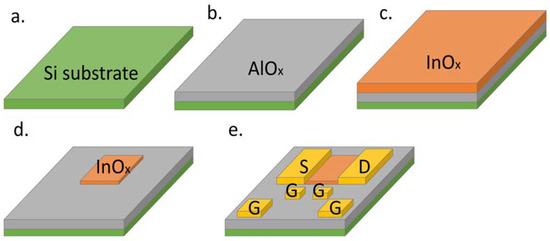
Figure 1.
(a–e). Fabrication schematic of multi-gate artificial synaptic transistor with InOx channel and AlOx electric-double-layer (EDL) dielectric. S, D, and G represent source, drain and gate.
3. Results and Discussion
Figure 2 shows the X-ray photoelectron spectroscopy (XPS, ESCALAB 250Xi spectrometer, Thermo Fisher Scientific, Waltham, MA, USA) O1s spectrum of the AlOx thin film. The O1s peak can be split into two peaks. The peak centered at 530.9 eV corresponds to the oxygen (OI) in the lattice site, and the peak centered at 532.2 eV corresponds to oxygen in hydroxide (OII) [32]. The area ratio of OII/(OI + OII) was calculated to be 34.6%, indicating a large number of hydrogen-related defects in the AlOx thin film. In general, hydrogen protons can act as mobile protons in a solid electrolyte. Figure 3 shows the transfer curve of the device with a single planar gate. The clear anticlockwise hysteresis loop indicates EDLT behavior. This can be explained by the slow movement of hydrogen protons in the AlOx layer. The drain current on/off ratio is estimated to be ~108. The top planar gate plays the same role as the bottom gate electrode. Combined with XPS analysis, the work mechanism of the planar multi-gate EDLT is shown in Figure 4. When a positive voltage is applied on the planar gate, the hydrogen protons will move to the interface between AlOx film and InOx channel, laterally. Meanwhile, the mirror charges will appear in the channel, forming a huge EDL capacitance and increasing the channel conductance. The EDLT can operate with planar gate through proton-related lateral coupling effect.
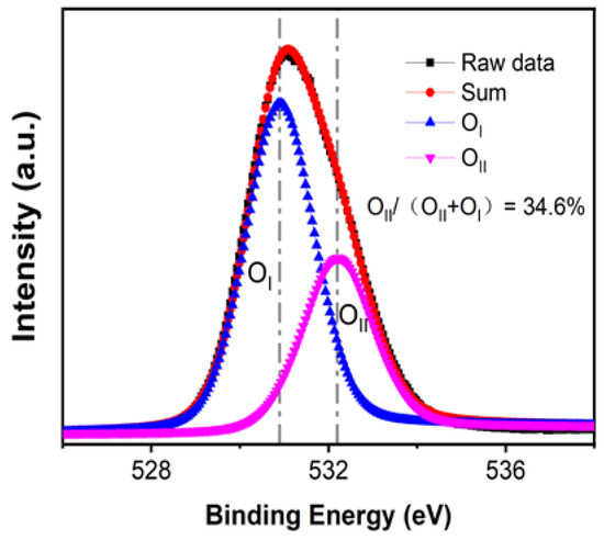
Figure 2.
The X-ray photoelectron spectroscopy (XPS) O1s spectrum of the AlOx EDL thin film.
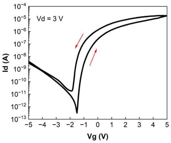
Figure 3.
Transfer curve of the AlOx/InOx electric-double-layer transistor (EDLT) with planar gate.
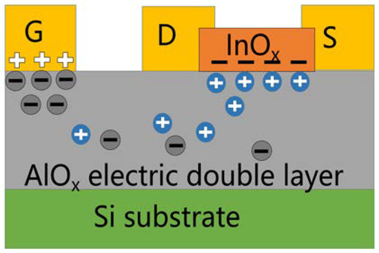
Figure 4.
Lateral coupling effect in AlOx/InOx EDLT with planar gate.
In order to investigate the synaptic behaviors of this EDLT, the EPSC was simulated with a single planar gate electrode. The spike applied on the gate represents the presynaptic spike, and the drain current represents the EPSC. During the test, Vds was set to a constant potential of 2 V. The presynaptic spike was applied on a planar gate with duration of 20 ms and various amplitudes ranging from 1 V to 5 V. As shown in Figure 5a, with the increase in the spike amplitude, the EPSC increases correspondingly. When the spike is over, the EPSC gradually decays back to the initial current. As we know, the EPSC is controlled by protons in EDL, which move into interface between electrolyte and semiconductor channel, or even partially enter into the channel, and diffuse back, resulting in charging and discharging of EDL capacitor [33,34]. The proton movement process can be described by the stretch index function with delay time [35]. So, the change in EPSC can be fitted by the following formula [35]:
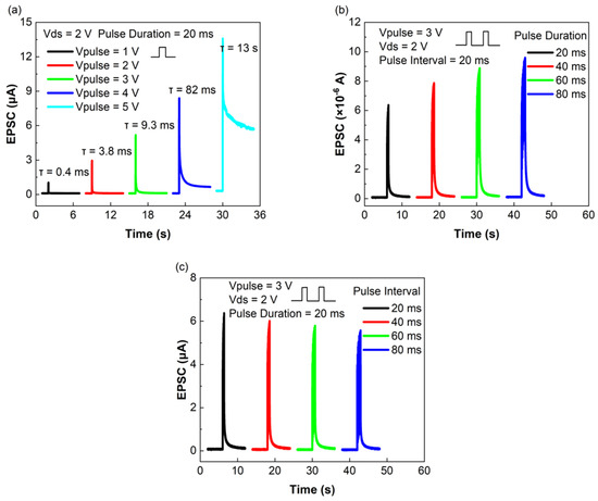
Figure 5.
Excitatory postsynaptic current (EPSC) curves of the AlOx/InOx EDLT with a planar gate controlled by (a) single pulse with various amplitudes, (b) 10 consecutive pulses with various durations, and (c) 10 consecutive pulses with various intervals.
τ is the retention time of EPSC decay. t0 is the time point at the end of the pulse. Ipeak is the peak value of current. I∞ is the resting state value of current, and β is the stretch index, ranging from 0 to 1. As shown in Figure 5a, the retention time (τ) for spike amplitude of 1 V is estimated to be about 0.4 ms by using Equation (1). When the spike amplitude increases to 5 V, the retention time (τ) extends to 13 s. It is worth mentioning that, 200 s later, after the end of the 5 V spike, the EPSC still stays a large value, and it is difficult to come back to the initial state. When a presynaptic spike is applied on the planar gate, the positive protons in AlOx will move to the interface between electrolyte and semiconductor channel, and then a lot of electrons will be accumulated in the channel. When the spike is over, the protons will diffuse back to the initial states. The movement of protons in the electrolyte takes time, which corresponds to STP. However, if higher amplitudes are applied, some of the mobile protons will enter into InOx channel under a strong electric field. This process is called electrochemical doping, reported in our previous work [22,31]. It is difficult for them to come back to their initial states, resulting in a long recovery time. The electrochemical doping in channel by protons during spike stimulation leads to the transition from STP to LTP.
The EPSC can be controlled by the number, duration, and interval of the pulse. As shown in Figure 5b,c, 10 consecutive pulses with amplitude of 3 V are used. The EPSC increases and tends to saturation with the increase in the pulse number. When the pulse duration is increased and the pulse interval is kept at 20 ms, the EPSC increases, as shown in Figure 5b. Similarly, when the pulse duration is kept at 20 ms, the EPSC decreases with the increase in the pulse interval, as shown in Figure 5c. The results indicate that the accumulation and relaxation of hydrogen protons in the semiconductor are dynamic processes. If the previous EPSC has not yet relaxed to its initial state before the arrival of the next pulse, the next EPSC will be enhanced. Increasing duration time can enhance the accumulation process and lead to the increase in the EPSC. In contrast, with the increase in the pulse interval time, protons have a long time to diffuse back, resulting in the decrease in the EPSC. As the number of pulses increases, the absorption and diffusion of protons will achieve a balance. As result, the EPSC tends to saturation.
In order to investigate the interaction between synapses, we chose two planar gates (G1 and G2) and applied 10 consecutive pulses with amplitude of 3 V, interval time of 80 ms, and duration of 20 ms on the gates to obtain EPSC. The pulses were applied on G1 or G2, respectively, or applied on G1 and G2, simultaneously. As shown in Figure 6, when the pulses are applied on G1 and G2, simultaneously, the EPSC at 10th pulse is 7.71 µA, which is larger than that of any single gate (5.73 µA for G1 and 4.69 µA for G2) when the pulses are applied. The result indicates that the output is not a simple linear superposition of each output facilitated by an individual gate electrode. It is a dynamic process. During this process, the artificial synapses aggregate inputs and change their synaptic weight.
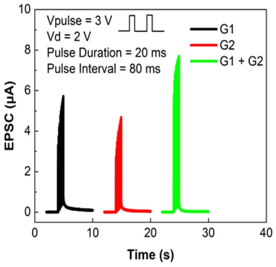
Figure 6.
EPSCs controlled by consecutive pulses applied on G1 or G2, respectively, and G1 and G2, simultaneously.
In a neural system, the weight of synapses is not the same. As a spatial resolution function, we have studied the effects of the presynaptic location and size on the synaptic functions. Here, 10 consecutive pulses with amplitude of 3 V, duration of 20 ms, and interval time of 80 ms were applied on planar gates with different distances to the channel and different areas. As shown in Figure 7a, the closer the gate is to the channel, the greater the EPSC is. For the case with distance of 820 µm, the EPSC at the 10th pulse is about 3.74 µA, and for the case with distance of 3820 µm, the EPSC at the 10th pulse is reduced to 2.59 µA. This result indicates that the lateral coupling effect of the capacitance is dependent on the distance between gate and channel, nonlinearly. When we keep the same distance and change the presynaptic area, as shown in Figure 7b, the larger the gate area is, the greater the EPSC is. The result indicates that the larger gate area contributes to the larger EDL capacitance. The spatial information can be emulated by the multi-gate synaptic transistor.
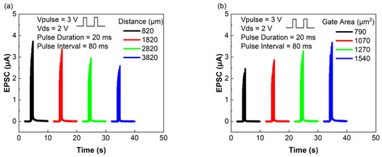
Figure 7.
EPSC curves of the multi-gate EDLT when the consecutive pulses are added on the planar gate electrodes with (a) different distances to the channel, (b) different areas.
As a form of short-term synaptic plasticity, PPF characteristic represents the dynamic enhancement of neurotransmitters in biological neural synapses and is involved in various neural tasks, such as simple learning and encoding temporal information [36]. The PPF behavior has been demonstrated by applying two consecutive pulses on planar gate with an interval time [37]. The PPF index is defined as the ratio of EPSC 2 (the post spike) to EPSC 1 (the first spike) [35]. We chose two planar gates (Gate1 and Gate2) to investigate the properties of PPF. It was mentioned that these two planar gates exhibit different EPSC characteristics. Figure 8 shows the PPF index, where two consecutive spikes with amplitude of 3 V and duration of 20 ms are applied by adjusting the interval time between the spikes. The shorter the interval between the two spikes, the more mobile the protons are when accumulating, before diffusing back, and the more PPF occurs. Considering the interaction of gates, two consecutive spikes are successively applied on two gates: the first spike is applied on Gate1, and the post spike is applied on Gate2, or in reverse order. As shown in Figure 8, the PPF index for the case that the first spike applied on Gate1 and post spike applied on Gate2 is quite different from the PPF index for the case with reverse order. The result indicates that the PPF index is based on time sequence. The temporal characteristics of inputs play an important role in output. It indicates that, compared with EDLT with single gate, the detecting function of time sequence can be achieved in the artificial synaptic transistor with coplanar multiple gates.
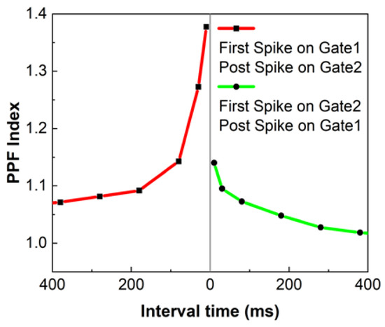
Figure 8.
Paired-pulse facilitation (PPF) index for the cases where the first pulse is applied on Gate1 and the second pulse is applied on Gate2, as well as its reverse.
4. Conclusions
In summary, the planar multi-gate artificial synaptic transistor was fabricated with solution-processed AlOx EDL and solution-processed InOx channel. The synaptic function of EPSC was emulated successfully by planar gate through lateral coupling effect. The EPSC is dependent on the planar gate location and area as spatial information. As for time information, the dependence of time sequence is demonstrated by PPF index of two planar gates. The multi-gate synaptic transistor, which can be used to simulate multi-dimensional information, will promote the development of complex neural networks.
Author Contributions
Conceptualization, Y.P.; methodology and analysis, Y.P., Y.L. and Z.L.; writing—original draft preparation, Y.L.; writing—review and editing, Y.L. and Y.P. All authors have read and agreed to the published version of the manuscript.
Funding
This work is supported in part by the National Key Research and Development Program of China (Grant No. 2021YFB3600701), and the Natural Science Foundation of China (Grant No. 61804187 and No.62074167), respectively.
Institutional Review Board Statement
Not applicable.
Informed Consent Statement
Not applicable.
Data Availability Statement
The data presented in this study are available upon request from the corresponding author.
Acknowledgments
The authors thank State Key Laboratory of Optoelectronic Materials and Technologies, School of Electronics and Information Technology, Sun Yat-Sen University for supplying the photolithography system, XPS system, and Agilent system.
Conflicts of Interest
The authors declare no conflict of interest.
References
- von Neumann, J. The principles of large-scale computing machines. Ann. Hist. Comput. 1989, 10, 243–256. [Google Scholar] [CrossRef]
- Chang, T.; Yang, Y.; Lu, W. Building Neuromorphic Circuits with Memristive Devices. IEEE Circuits Syst. Mag. 2013, 13, 56–73. [Google Scholar] [CrossRef]
- Drachman, D.A. Do we have brain to spare? Neurology 2005, 64, 2004–2005. [Google Scholar] [CrossRef] [PubMed]
- Furber, S. Large-scale neuromorphic computing systems. J. Neural Eng. 2016, 13, 051001. [Google Scholar] [CrossRef] [PubMed]
- Furber, S. To Build a Brain. IEEE Spectr. 2012, 49, 44–49. [Google Scholar] [CrossRef]
- Yang, R.; Huang, H.-M.; Hong, Q.-H.; Yin, X.-B.; Tan, Z.-H.; Shi, T.; Zhou, Y.-X.; Miao, X.-S.; Wang, X.-P.; Mi, S.-B.; et al. Synaptic Suppression Triplet-STDP Learning Rule Realized in Second-Order Memristors. Adv. Funct. Mater. 2018, 28, 1704455. [Google Scholar] [CrossRef]
- Choquet, D.; Triller, A. The Dynamic Synapse. Neuron 2013, 80, 691–703. [Google Scholar] [CrossRef]
- Kuzum, D.; Yu, S.; Wong, H.S.P. Synaptic electronics: Materials, devices and applications. Nanotechnology 2013, 24, 382001. [Google Scholar] [CrossRef]
- Hu, L.; Fu, S.; Chen, Y.; Cao, H.; Liang, L.; Zhang, H.; Gao, J.; Wang, J.; Zhuge, F. Ultrasensitive Memristive Synapses Based on Lightly Oxidized Sulfide Films. Adv. Mater. 2017, 29, 1606927. [Google Scholar] [CrossRef]
- Yu, H.; Gong, J.; Wei, H.; Huang, W.; Xu, W. Mixed-halide perovskite for ultrasensitive two-terminal artificial synaptic devices. Mater. Chem. Front. 2019, 3, 941–947. [Google Scholar] [CrossRef]
- Kuzum, D.; Jeyasingh, R.G.D.; Lee, B.; Wong, H.S.P. Nanoelectronic Programmable Synapses Based on Phase Change Materials for Brain-Inspired Computing. Nano Lett. 2012, 12, 2179–2186. [Google Scholar] [CrossRef] [PubMed]
- Chen, Y.; Yu, H.; Gong, J.; Ma, M.; Han, H.; Wei, H.; Xu, W. Artificial synapses based on nanomaterials. Nanotechnology 2019, 30, 012001. [Google Scholar] [CrossRef] [PubMed]
- Nishitani, Y.; Kaneko, Y.; Ueda, M.; Morie, T.; Fujii, E. Three-terminal ferroelectric synapse device with concurrent learning function for artificial neural networks. J. Appl. Phys. 2012, 111, 124108. [Google Scholar] [CrossRef]
- Han, H.; Yu, H.; Wei, H.; Gong, J.; Xu, W. Recent Progress in Three-Terminal Artificial Synapses: From Device to System. Small 2019, 15, e1900695. [Google Scholar] [CrossRef] [PubMed]
- Qian, C.; Kong, L.-a.; Yang, J.; Gao, Y.; Sun, J. Multi-gate organic neuron transistors for spatiotemporal information processing. Appl. Phys. Lett. 2017, 110, 083302. [Google Scholar] [CrossRef]
- John, R.A.; Ko, J.; Kulkarni, M.R.; Tiwari, N.; Nguyen Anh, C.; Ing, N.G.; Leong, W.L.; Mathews, N. Flexible Ionic-Electronic Hybrid Oxide Synaptic TFTs with Programmable Dynamic Plasticity for Brain-Inspired Neuromorphic Computing. Small 2017, 13, 1701193. [Google Scholar] [CrossRef]
- Du, H.W.; Lin, X.; Xu, Z.M.; Chu, D.W. Electric double-layer transistors: A review of recent progress. J. Mater. Sci. 2015, 50, 5641–5673. [Google Scholar] [CrossRef]
- Tian, H.; Mi, W.; Wang, X.-F.; Zhao, H.; Xie, Q.-Y.; Li, C.; Li, Y.-X.; Yang, Y.; Ren, T.-L. Graphene Dynamic Synapse with Modulatable Plasticity. Nano Lett. 2015, 15, 8013–8019. [Google Scholar] [CrossRef]
- Zhou, J.; Liu, N.; Zhu, L.; Shi, Y.; Wan, Q. Energy-Efficient Artificial Synapses Based on Flexible IGZO Electric-Double-Layer Transistors. IEEE Electron Device Lett. 2015, 36, 198–200. [Google Scholar] [CrossRef]
- Wan, X.; Yang, Y.; Feng, P.; Shi, Y.; Wan, Q. Short-Term Plasticity and Synaptic Filtering Emulated in Electrolyte-Gated IGZO Transistors. IEEE Electron Device Lett. 2016, 37, 299–302. [Google Scholar] [CrossRef]
- Wen, J.; Zhu, L.Q.; Fu, Y.M.; Xiao, H.; Guo, L.Q.; Wan, Q. Activity Dependent Synaptic Plasticity Mimicked on Indium-Tin-Oxide Electric-Double-Layer Transistor. Acs Appl. Mater. Interfaces 2017, 9, 37064–37069. [Google Scholar] [CrossRef]
- Liang, X.C.; Luo, Y.Y.; Pei, Y.L.; Wang, M.Y.; Liu, C. Multimode transistors and neural networks based on ion-dynamic capacitance. Nat. Electron. 2022, 5, 859–869. [Google Scholar] [CrossRef]
- Dai, S.; Wang, Y.; Zhang, J.; Zhao, Y.; Xiao, F.; Liu, D.; Wang, T.; Huang, J. Wood-Derived Nanopaper Dielectrics for Organic Synaptic Transistors. Acs Appl. Mater. Interfaces 2018, 10, 39983–39991. [Google Scholar] [CrossRef] [PubMed]
- Liu, Y.H.; Zhu, L.Q.; Feng, P.; Shi, Y.; Wan, Q. Freestanding Artificial Synapses Based on Laterally Proton-Coupled Transistors on Chitosan Membranes. Adv. Mater. 2015, 27, 5599–5604. [Google Scholar] [CrossRef] [PubMed]
- Wang, J.; Li, Y.; Yang, Y.; Ren, T.-L. Top-Gate Electric-Double-Layer IZO-Based Synaptic Transistors for Neuron Networks. IEEE Electron Device Lett. 2017, 38, 588–591. [Google Scholar] [CrossRef]
- He, Y.; Yang, Y.; Nie, S.; Liu, R.; Wan, Q. Electric-double-layer transistors for synaptic devices and neuromorphic systems. J. Mater. Chem. C 2018, 6, 5336–5352. [Google Scholar] [CrossRef]
- Zhu, L.Q.; Xiao, H.; Liu, Y.H.; Wan, C.J.; Shi, Y.; Wan, Q. Multi-gate synergic modulation in laterally coupled synaptic transistors. Appl. Phys. Lett. 2015, 107, 143502. [Google Scholar] [CrossRef]
- Li, S.; Lyu, H.; Li, J.; He, Y.; Gao, X.; Wan, Q.; Shi, Y.; Pan, L. Multiterminal Ionic Synaptic Transistor with Artificial Blink Reflex Function. IEEE Electron Device Lett. 2021, 42, 351–354. [Google Scholar] [CrossRef]
- Wang, X.; Zhu, L.; Chen, C.; Mao, H.; Zhu, Y.; Zhu, Y.; Yang, Y.; Wan, C.; Wan, Q. Freestanding multi-gate IZO-based neuromorphic transistors on composite electrolyte membranes. Flex. Print. Electron. 2021, 6, 044008. [Google Scholar] [CrossRef]
- Liang, X.; Li, Z.; Liu, L.; Chen, S.; Wang, X.; Pei, Y. Artificial synaptic transistor with solution processed InOx channel and AlOx solid electrolyte gate. Appl. Phys. Lett. 2020, 116, 012102. [Google Scholar] [CrossRef]
- Liang, X.; Liu, L.; Cai, G.; Yang, P.; Pei, Y.; Liu, C. Evidence for Pseudocapacitance and Faradaic Charge Transfer in High-Mobility Thin-Film Transistors with Solution-Processed Oxide Dielectrics. J. Phys. Chem. Lett. 2020, 11, 2765–2771. [Google Scholar] [CrossRef] [PubMed]
- Xu, W.Y.; Wang, H.; Xie, F.Y.; Chen, J.; Cao, H.T.; Xu, J.B. Facile and Environmentally Friendly Solution-Processed Aluminum Oxide Dielectric for Low-Temperature, High-Performance Oxide Thin-Film Transistors. Acs Appl. Mater. Interfaces 2015, 7, 5803–5810. [Google Scholar] [CrossRef] [PubMed]
- Kornyshev, A.A. Double-layer in ionic liquids: Paradigm change? J. Phys. Chem. B 2007, 111, 5545–5557. [Google Scholar] [CrossRef] [PubMed]
- Kim, S.H.; Hong, K.; Xie, W.; Lee, K.H.; Zhang, S.P.; Lodge, T.P.; Frisbie, C.D. Electrolyte-Gated Transistors for Organic and Printed Electronics. Adv. Mater. 2013, 25, 1822–1846. [Google Scholar] [CrossRef] [PubMed]
- Zhu, L.Q.; Wan, C.J.; Guo, L.Q.; Shi, Y.; Wan, Q. Artificial synapse network on inorganic proton conductor for neuromorphic systems. Nat. Commun. 2014, 5, 3158. [Google Scholar] [CrossRef] [PubMed]
- Buonomano, D.V.; Maass, W. State-dependent computations: Spatiotemporal processing in cortical networks. Nat. Rev. Neurosci. 2009, 10, 113–125. [Google Scholar] [CrossRef]
- Atluri, P.P.; Regehr, W.G. Determinants of the time course of facilitation at the granule cell to Purkinje cell synapse. J. Neurosci. 1996, 16, 5661–5671. [Google Scholar] [CrossRef]
Disclaimer/Publisher’s Note: The statements, opinions and data contained in all publications are solely those of the individual author(s) and contributor(s) and not of MDPI and/or the editor(s). MDPI and/or the editor(s) disclaim responsibility for any injury to people or property resulting from any ideas, methods, instructions or products referred to in the content. |
© 2023 by the authors. Licensee MDPI, Basel, Switzerland. This article is an open access article distributed under the terms and conditions of the Creative Commons Attribution (CC BY) license (https://creativecommons.org/licenses/by/4.0/).