Article

Failure Analysis of Printed Circuit Board Solder Joint under Thermal Shock

1
School of Materials Science and Engineering, Jiangsu University of Science and Technology, Zhenjiang 212003, China
2
Shanghai Motor Vehicle Inspection Certification and Tech Innovation Center Co., Ltd., Shanghai 201805, China
*
Authors to whom correspondence should be addressed.
Coatings 2023, 13(3), 572; https://doi.org/10.3390/coatings13030572
Submission received: 11 February 2023 / Revised: 27 February 2023 / Accepted: 28 February 2023 / Published: 7 March 2023

Abstract

:
Investigating the failure mechanism of solder joints under different temperature conditions is significant to ensure the service life of a printed circuit board (PCB). In this research, the stress and strain distribution of a PCB solder joint was evaluated by high- and low-temperature thermal shock tests. The cross-section of the solder joint after thermal shock testing was measured using a 3D stereoscopic microscope and SEM equipped with EDS. The microstructure of the lead-free solder joint and the phase of the intermetallic compound (IMC) layer were studied by XRD. The working state of the PCB solder joint under thermal shock was simulated and analyzed by the finite element method. The results show that thermal shock has a great effect on the reliability of solder joints. The location of the actual crack is consistent with the maximum stress–strain concentration area of the simulated solder joint. The brittle Cu6Sn5 and Cu3Sn phases at the interface accelerate the failure of solder joints. Limiting the growth of Cu6Sn5 and Cu3Sn phases can improve the reliability of solder joints to a certain extent.

1. Introduction

Printed circuit boards (PCB) [1,2,3,4] can provide necessary mechanical support for various components in the circuit, and have become an important part of electronic products. In addition, PCBs have the characteristics of high set neutrality, and high reliability, which is also convenient for daily production, design and maintenance. Using PCBs can greatly improve the level of mechanical automation and product production efficiency. Based on the above, PCBs have been extensively employed in computers, automotive, aerospace, and other industries.
At present, the solder used in PCB manufacture is mainly lead-free solder [5,6,7,8,9,10]. The most commonly used lead-free solders mainly include Sn-Ag [11,12,13,14], Sn-Cu [15,16,17,18], Sn-Zn [19,20,21,22], and Sn-Ag-Cu (SAC) [23,24,25]. SAC305 solder [26] is widely used because of its high performance and low cost. The reliability of solder joints is one of the important research directions in the field of electronic packaging. The reliability of a PCB board usually depends on the life of its solder joints. The PCB solder joint is a weak part of the entire electronic product. It is prone to crack initiation, propagation, and even fractures in harsh environments such as high-temperature, low-temperature, and violent vibration environments [27]. Voids and cracks cause damage to the pins of electronic components, adversely affecting the reliability of their solder joints and even seriously reducing the service life of the PCB board [28,29,30]. According to existing research, solder joint failure is responsible for nearly 60% of electronic product failures [31]. The PCB industry has developed towards high precision, high density, and high reliability in recent years, which further puts higher demands on PCB process reliability. Therefore, it is crucial to study the reliability of PCB solder joints.
In this research, the stress and strain distributions of PCB solder joints under high- and low-temperature thermal shock tests were evaluated by experiments and finite element simulation, respectively. The failure mechanism of PCB solder joints was discussed based on the comparative study between finite element simulation and experimental research. ANSYS simulation and specific experiments were combined to analyze PCB board failure. Micromorphology observation and phase analysis of PCB solder failure parts were performed. The failure mechanisms of SAC305, a commonly used joint solder in the industry, under thermal shock are summarized. This study can provide a basis for the analysis of possible failures in PCB board manufacturing and use.

2. Methods

2.1. Research Object

The PCB pin components included copper parts with excellent electronic properties. The solder used in this experiment was a lead-free silver solder, SAC305 solder [26], which consisted of 96.5% tin, 3% silver, and 0.5% copper. The components studied in this paper were 0603 resistors of the square flat package (QFP) [32], which were installed on a 2 mm thick PCB made of epoxy resin board (FR4) [33].

2.2. Thermal Shock Test

The thermal shock test was carried out in a self-made device equipped with a muffle furnace (Sante, Luoyang, China) and a freezer (Haier, Qingdao, China). The test conditions were based on the standards specified in GB2423.22. The temperature range of the test was set to −18–155 °C. The time of temperature change was set at 2 min, and the temperature was kept at −18 and 155 °C for 2 h (10 cycles), respectively. The thermal shock test was loaded for 10 cycles. The temperature loading curve used in the thermal shock test is shown in Figure 1.

2.3. Finite Element Analysis

ANSYS is a commonly used simulation software [34,35,36,37,38]. In order to simulate finite elements, the coarse and fine mesh method was utilized. The finite element analysis of the model was carried out in a global and local manner. SolidWorks software (version 2022) was used to model the entire component and solder joint after establishing the overall temperature impact model. The analysis simulation was conducted using ANSYS analysis software (ANSYS 14.5).
As shown in Figure 2a, the PCB single-component graphic was created using SolidWorks software (version 2022) based on dimensional criteria. Figure 2b shows the single-component finite element mesh model created using ANSYS software. The specific thermodynamic parameters are listed in Table 1.
The model was simulated and the stress–strain diagram of the solder joints in the corresponding temperature range was obtained. Mises criterion was used to analyze the thermal shock stress–strain behavior of the solder joints. The equivalent stress and equivalent strain were used to analyze the internal stress–strain distribution.
The relationship between the equivalent force and the stress tensor is shown in the following equation [39].
σ = 2 2 σ x σ y + σ y σ z + σ x σ z + 6 τ x y 2 + τ y z 2 + τ x z 2 1 2
σ is the equivalent force, Pa (Pascal); σx, σy, σz are the positive stresses in the X, Y, and Z directions, respectively; τxy is the shear stress in the Y-axis direction perpendicular to the X-axis plane, Pa; τyz is the shear stress perpendicular to the Z-axis plane of the Y-axis, Pa; τxz is the shear stress perpendicular to the Z-axis plane of the X-axis, Pa.
The relationship between the equivalent variation effect and the strain tensor components is shown in the following equation.
ε = 2 3 ε x ε y 2 + ε y ε z 2 + ε x ε z 2 + 3 2 γ x y 2 + γ y z 2 + γ x z 2 1 2
Among them, ε is the equivalent value; εx, εy, εz are positive strains in the X, Y, and Z directions, respectively; γxy is the shear strain in the Y-axis direction perpendicular to the X-axis plane; γyz is the shear strain in the Z-direction perpendicular to the Y-plane plane; γxz is the shear strain perpendicular to the Z-axis plane in the X-axis plane.

2.4. Characterization

Observation of the internal topography was achieved by industrial CT (YXLON FF35CT) at the operating power of 320 W. The microstructure and elemental composition were characterized by scanning electron microscopy (SEM, Regulus-8100, Hitachi, Tokyo, Japan) and energy dispersive spectroscopy (EDS, Pro X, Phenom, Eindhoven, The Netherlands). An X-ray diffractometer (Bruker D2 phaser, Bruker, Karlsruhe, Germany) was used to test the phase composition at cross-section cracks. The diffraction angle 2θ ranged from 30° to 100°. DIFFRAC (SUITE) and Jade6.0 software were used to calibrate the phase of the solder cracks.

3. Results and Discussion

3.1. Morphology of Solder Joints

Figure 3 shows the industrial computed tomography (CT) images of the PCB board sample. The solder joints of the PCB are well-formed and neatly arranged. Moreover, the solder joints have no obvious damage marks and are spread in a streamlined pattern. The processor generates a significant amount of heat when operating under high loads. This extreme environment can easily cause solder joint failure [40]. To ensure the functional reliability of PCBs under harsh environmental conditions, thermal shock experiments are designed and studied to explore the failure mechanism of PCB solder joints in harsh environments.

3.2. Finite Element Analysis

Specific dimensions of the PCB resistance components were measured and the finite element analysis model was established using ANSYS. Finite element analysis was accomplished according to the thermodynamic parameters of the substrate, components, Cu lead, and solder. Nephograms of stress and strain were obtained, and the distribution of stress and strain at different temperatures was analyzed. The 3D solid model was then divided into 3D solid meshes. The model contains 69,108 nodes and 30,993 cells after meshing. The solder of the model was identified as linear material, and the linear unit Solid 45 was used. The physical parameters were considered to be isotropic. It was assumed that the structure of the material was uniform without segregation, the welding interface was in good contact, and there were no defects such as pores and holes. The temperature of each area of the model was the same, and the influence of partial temperature non-uniformity caused by the difference in the convective heat transfer coefficient of each material was ignored.
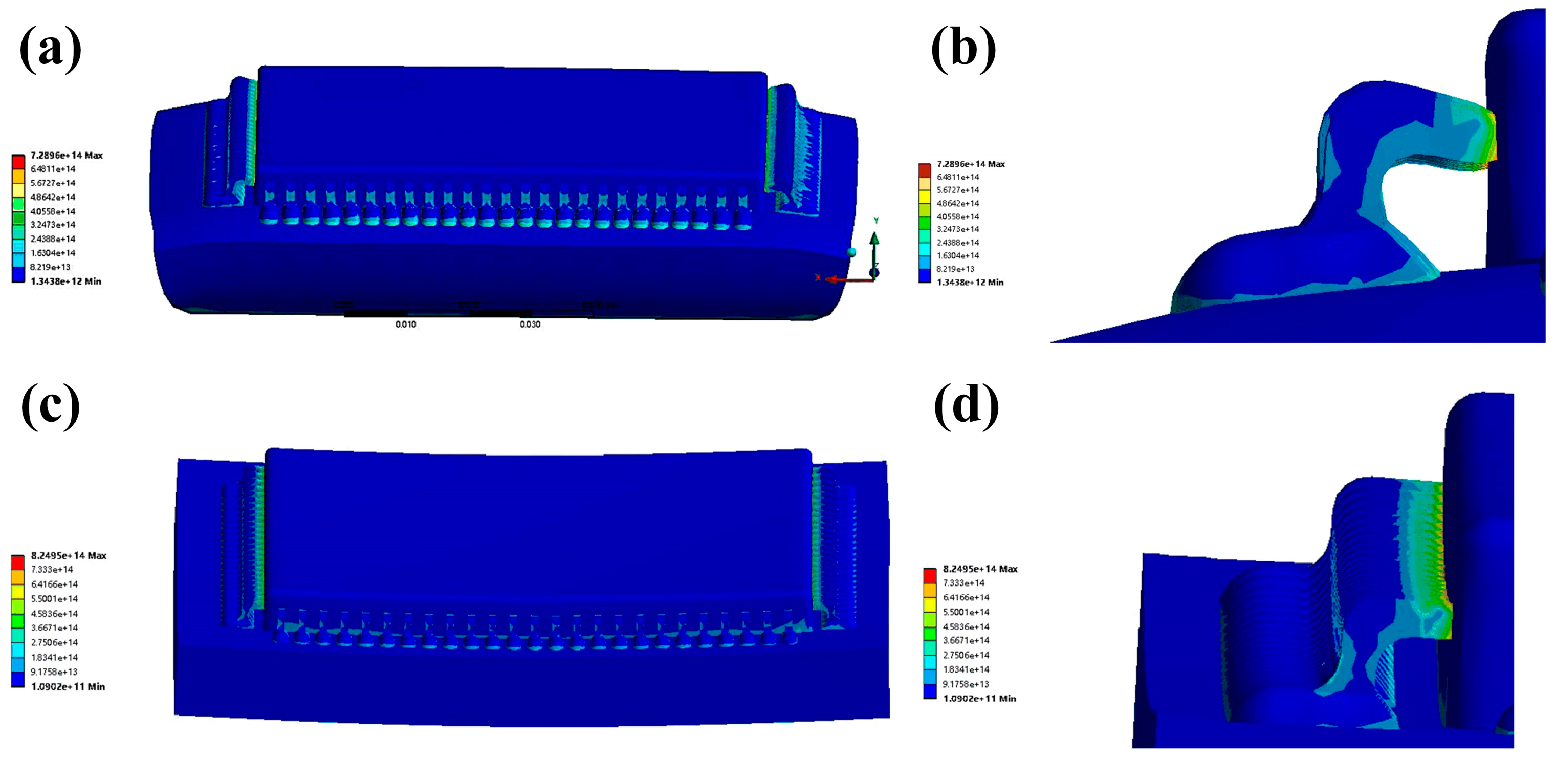
In the process of thermal shock, the three-dimensional structural stress distribution of the solder joint is multi-axial. The equivalent stress profile of each component is shown in Figure 4. The stress distribution of the left and right solder joints is roughly the same. The stress generated at the interface of each component is greater than that generated in the component. The connection between the components and Cu lead, the connection between the solder joint and Cu plate, and the interface between the solder and Cu lead represent typical locations where defects can easily occur.
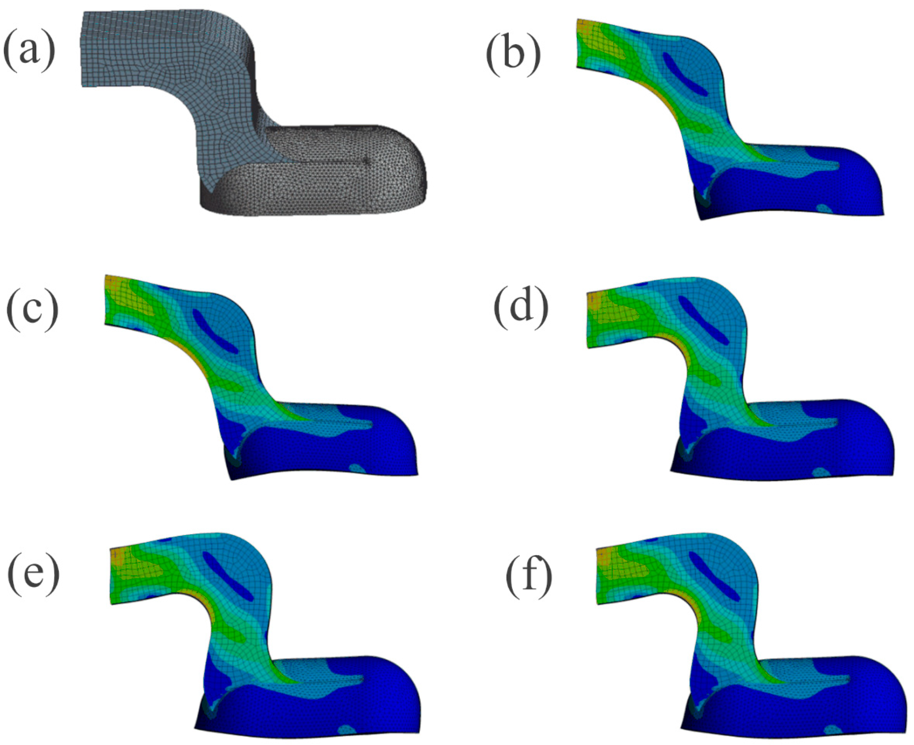
Figure 5 shows the grid segmentation analysis diagram of solder joints at high and low temperatures. In Figure 5, it is evident that a single solder joint is prone to failure at the junction of the solder and copper plate and the junction of the Cu wire and solder. After being subjected to obvious thermal expansion and contraction, the interface between the solder, Cu lead and Cu bottom disk is prone to generate a high stress value and increase the risk of failure. The stress distribution in the solder joint is uneven. The contact surface between the solder joint and the components is subjected to the maximum stress value, which is close to the junction of the solder, components, and pads. There is a certain area of high stress at the top when the temperature is −18 °C, as shown in Figure 5b. This area becomes smaller and smaller as the temperature increases. When the temperature reaches 80 °C, the high-stress concentration decreases and the stress tends to average out, as shown in Figure 5e. In addition, the stress concentration begins to slowly increase at the edge, and the area grows larger as the temperature increases. It can be predicted that the top of the joint between the solder and the components is also a position prone to defects. Fractures are more likely to develop and cause solder joint failure when the joint is in use at low temperatures. Defects between the solder and components on either side of the joint may also occur during service at high temperatures, reducing the reliability of the solder joint.
The temperature of zero stress is set at 22 °C, and the stress value decreases first and then increases with the increase in temperature. The maximum and minimum stress values at each temperature are shown in Table 2. Under actual working conditions, plastic deformation occurs in the solder joint. The greater the cyclic stress, the higher the plastic deformation, and the easier the solder joint will fail. The stress distribution diagram shows that the more extreme the difference in temperature between high and low temperatures, the more likely it is that failure will occur.
The maximum and minimum strain values at each temperature are shown in Table 3. As the temperature increases, the solder joint strain decreases first and then increases. The solder joint demonstrates different types of deformation under different temperature impact conditions. At high temperatures, the solder joint expands when heated, and the solder joint exerts “extrusion pressure” on the components and pads. At low temperatures, the solder joint contracts when it is cold, and the solder joint exerts tensile stress on the components and pads. Since solder is defined as an elastic material, the strain diagram of the solder joint is almost the same as the stress diagram. The internal strain distribution is uneven. The interface between the component and the Cu pad is the maximum strain area, which is consistent with the stress diagram. As the temperature increases, the high strain zone gradually moves to both sides and the strain distribution gradually becomes uniform.

3.3. Thermal Shock Analysis

After the thermal shock, the cross-section of the solder joint can be observed in Figure 6. It can be observed that the crack occurs at the interface between the filler metal and the Cu lead wire and the joint between the filler metal and the Cu bottom plate. In the process of thermal shock, cyclic tensile and compressive stresses are generated between the solder joint and the copper plate, due to the different thermal expansion coefficients between the solder joint and the copper plate. This will also lead to uneven shrinkage or expansion of each component, resulting in a large concentration of stress at the interface, causing cracks and accelerating material failure. Meanwhile, the increase in intermetallic compound (IMC) layer thickness will also affect the joint strength between the solder joint and the copper plate. According to the EDS analysis in Figure 6c,d, Cu and Sn elements appear in the area of points a and d (IMC layer) [41]. The mass ratio of Cu to Sn at point a is about 1:3. Correspondingly, the mass ratio of Cu to Sn at point d is about 1:4. There is a mixture of Cu and Sn in this area. The solder is affected by the accumulated residual stress during the thermal shock. Stress shows an increasing trend at the heating stage. The maximum stress concentration occurred at the 155 °C insulation stage. Due to stress relaxation during the cooling process, stress on the pin and interface is released. Under the impact load of temperature, the internal stress of the solder joint changes periodically. When the temperature sharply drops, the stress of the solder joint sharpy increases due to the increase in the thermal expansion ratio. During the insulation process at −18 °C, the stress minimally changes and there is no obvious stress relaxation. The stress change caused by thermal expansion and contraction is the main reason for solder joint failure.
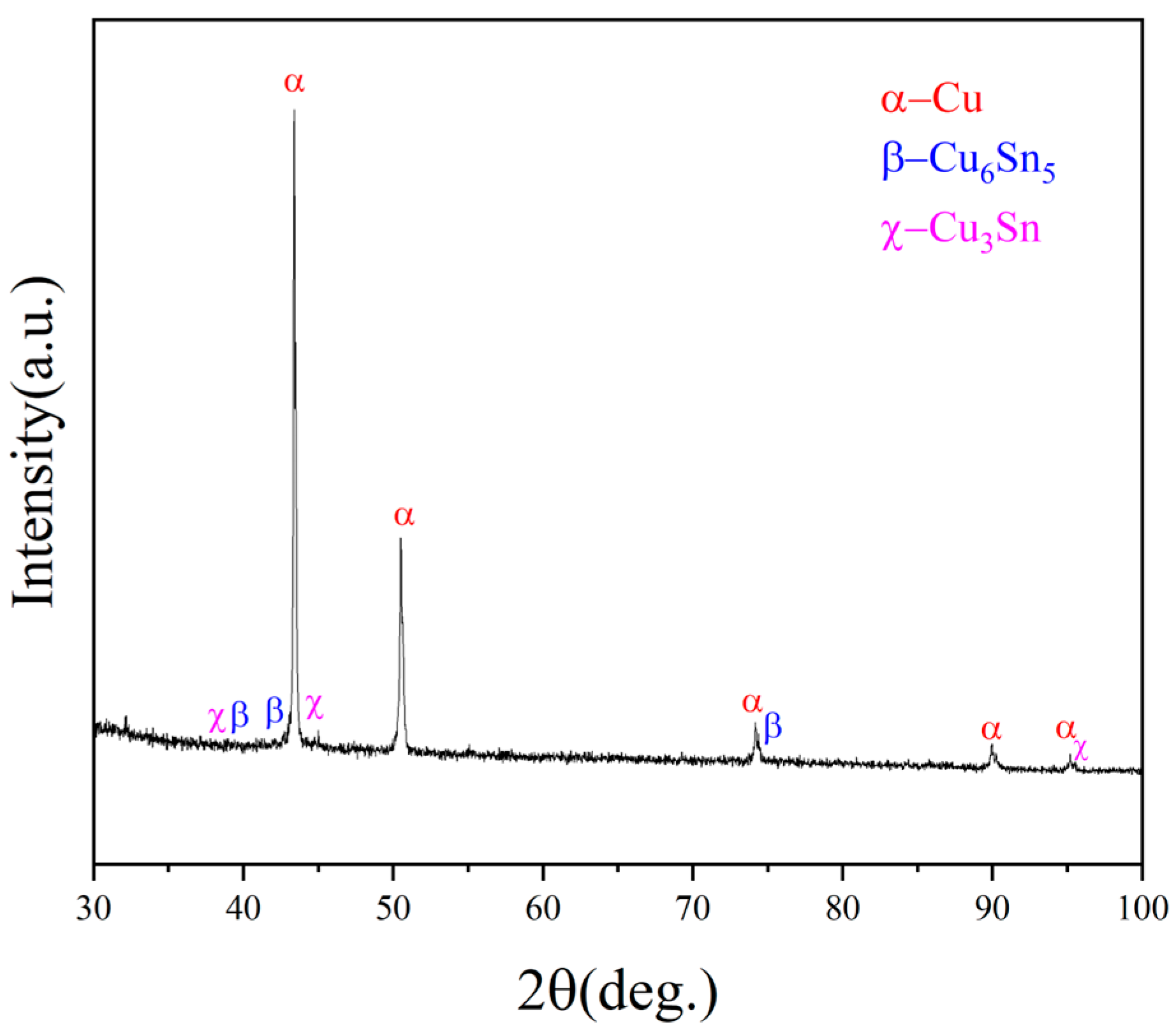
Figure 7 shows the XRD analysis at the cross-section of the solder joint. Cu6Sn5 (6Cu + 5Sn → Cu6Sn5) [42] was formed on an IMC layer during thermal shock. During the heat preservation process, the Cu6Sn5 phase gradually grows with the extension of the reaction time. The Cu substrate reacts with Cu6Sn5 in the IMC layer to generate Cu3Sn (Cu6Sn5 + 9Cu → 5Cu3Sn) [42], which is very thin and accounts for a small proportion overall. As the reaction continues, the fusion of Sn and Cu substrates intensifies, and Cu6Sn5 accounts for a much higher proportion in the IMC layer compared to Cu3Sn [43]. Cu6Sn5 and Cu3Sn easily cause cracks in the stress concentration process due to their hardness and fragility, which is detrimental to the bond strength of solder joints.
Figure 8 shows the failure mechanism of the PCB solder joint. The solder joint is affected by stress and small cracks are first produced in the IMC layer during the thermal shock process. With continuous thermal shock, cracks grow along the IMC layer, and eventually form larger cracks. These cracks are the main source of solder joint failure.

4. Conclusions

In this study, the failure mechanism of SAC305 joint solder under thermal shock was analyzed by combining an ANSYS simulation and experiment. Improvement measures were put forward according to the problems of solder joints under thermal shock conditions.
  • When a PCB board is subjected to thermal shock, the difference in the thermal expansion coefficient between Cu and solder will lead to a high stress concentration.
  • Cracks at the solder/Cu lead interface and the solder/Cu bottom plate joint are the main reasons for solder joint failure.
  • The simulation results show that the crack location is consistent with the position of the maximum stress and strain of the simulated solder joint.
  • The formation and growth of brittle Cu6Sn5 and Cu3Sn phases at the interface accelerated the failure of solder joints.
  • Reducing the use of PCBs in −18 to 155 °C thermal shock environments effectively avoids solder joint failure caused by Cu6Sn5 and Cu3Sn phase precipitation.

Author Contributions

Conceptualization, Z.Z. and Y.W.; methodology, Z.Z.; software, C.Y.; validation, Z.Z., C.Y., and Y.W.; formal analysis, C.Y.; investigation, Z.Z.; resources, Y.Z.; data curation, Z.Z.; writing—original draft preparation, Z.Z.; writing—review and editing, Z.Z.; visualization, J.C.; supervision, Y.Z.; project administration, Y.W.; funding acquisition, Y.W. All authors have read and agreed to the published version of the manuscript.

Funding

The authors are grateful for the financial support provided by the Shanghai Motor Vehicle Inspection Certification & Tech Innovation Center Co., Ltd., Jiangsu Provincial Natural Science Fund Research Project (grant number BK20211344), Jiangsu Provincial Six Talent Peaks (grant number 2018XCL-028) and Jiangsu Provincial Postgraduate Research & Practice Innovation Program (grant number KYCX21_3451).

Institutional Review Board Statement

Not applicable.

Informed Consent Statement

Not applicable.

Data Availability Statement

Not applicable.

Conflicts of Interest

The authors declare no conflict of interest.

References

  1. Alshihmani, H.; Maghrebi, M.-J.; Sardarabadi, M. Thermal performance prediction of a phase change material based heat-sink cooling system for a printed circuit board, using response surface method. J. Energy Storage 2022, 55, 105499. [Google Scholar] [CrossRef]
  2. Atintoh, A.; Kpobie, W.; Bonfoh, N.; Fendler, M.; Addiego, F.; Lipinski, P. Multiscale characterization of the mechanical behavior of a printed circuit board (PCB). Mater. Today Commun. 2023, 34, 104968. [Google Scholar] [CrossRef]
  3. Kumar, V.; Gupta, M. Comparative study of different natural fibre printed circuit board (PCB) composites. Mater. Today Proc. 2021, 44, 2097–2101. [Google Scholar] [CrossRef]
  4. Tang, J.; Wan, X.; Zhang, L. A sustainable printed circuit board derived hierarchically porous carbon/polyaniline composites for supercapacitors. Ceram. Int. 2022. [Google Scholar] [CrossRef]
  5. Kumar, N.; Maurya, A. Development of lead free solder for electronic components based on thermal analysis. Mater. Today Proc. 2022, 62, 2163–2167. [Google Scholar] [CrossRef]
  6. Li, Q.; Zhao, M.; Lin, J.; Lu, S. Effect of temperature on the corrosion behavior of lead-free solders under polyvinyl chloride fire smoke atmosphere. J. Mater. Res. Technol. 2021, 15, 3088–3098. [Google Scholar] [CrossRef]
  7. Xiao, J.; Tong, X.; Liang, J.; Chen, Q.; Tang, Q. Microstructure and morphology of the soldering interface of Sn–2.0Ag–1.5Zn low Ag content lead-free solder ball and different substrates. Heliyon 2023, 9, e12952. [Google Scholar] [CrossRef]
  8. Yahaya, M.Z.; Nazeri, M.F.M.; Salleh, N.A.; Kurt, A.; Kheawhom, S.; Illés, B.; Skwarek, A.; Abdullah, A.M.; Mohamad, A.A. Selective etching of lead-free solder alloys: A brief review. Mater. Today Commun. 2022, 33, 104520. [Google Scholar] [CrossRef]
  9. Chen, J.; He, Z.; Liu, J.; Wang, Y.; Hodgson, M.; Gao, W. Antibacterial anodic aluminium oxide-copper coatings on aluminium alloys: Preparation and long-term antibacterial performance. Chem. Eng. J. 2023, 461, 141873. [Google Scholar] [CrossRef]
  10. Wang, D.; Chen, G.; Wang, A.; Wang, Y.; Qiao, Y.; Liu, Z.; Qi, Z.; Liu, C.T. Corrosion behavior of single- and poly-crystalline dual-phase TiAl-Ti3Al alloy in NaCl solution. Int. J. Miner. Metall. Mater. 2023, 30, 689–696. [Google Scholar] [CrossRef]
  11. Amagai, M. A study of nanoparticles in Sn–Ag based lead free solders. Microelectron. Reliab. 2008, 48, 1–16. [Google Scholar] [CrossRef]
  12. Niranjani, V.; Rao, B.C.; Sarkar, R.; Kamat, S. The influence of addition of nanosized molybdenum and nickel particles on creep behavior of Sn–Ag lead free solder alloy. J. Alloys Compd. 2012, 542, 136–141. [Google Scholar] [CrossRef]
  13. Tunthawiroon, P.; Kanlayasiri, K. Effects of Ag contents in Sn–xAg lead-free solders on microstructure, corrosion behavior and interfacial reaction with Cu substrate. Trans. Nonferrous Met. Soc. China 2019, 29, 1696–1704. [Google Scholar] [CrossRef]
  14. Wang, Y.; Hu, B.; Tay, S.L.; Hou, F.; Gao, W.; Xiong, C. The microstructure and properties of sol-enhanced Sn–TiO2 nanocomposite coatings. Int. J. Mod. Phys. B 2017, 31, 1744025. [Google Scholar] [CrossRef]
  15. Freitas, E.S.; Osório, W.R.; Spinelli, J.E.; Garcia, A. Mechanical and corrosion resistances of a Sn–0.7wt.%Cu lead-free solder alloy. Microelectron. Reliab. 2014, 54, 1392–1400. [Google Scholar] [CrossRef]
  16. Kanlayasiri, K.; Mookam, N. Influence of Cu content on microstructure, grain orientation and mechanical properties of Sn–xCu lead-free solders. Trans. Nonferrous Met. Soc. China 2022, 32, 1226–1241. [Google Scholar] [CrossRef]
  17. Qu, D.; Li, C.; Bao, L.; Kong, Z.; Duan, Y. Structural, electronic, and elastic properties of orthorhombic, hexagonal, and cubic Cu3Sn intermetallic compounds in Sn–Cu lead-free solder. J. Phys. Chem. Solids 2020, 138, 109253. [Google Scholar] [CrossRef]
  18. Gao, W.; Cao, D.; Jin, Y.; Zhou, X.; Cheng, G.; Wang, Y. Microstructure and properties of Cu-Sn-Zn-TiO2 nano-composite coatings on mild steel. Surf. Coat. Technol. 2018, 350, 801–806. [Google Scholar] [CrossRef] [Green Version]
  19. El-Daly, A.; Hammad, A. Elastic properties and thermal behavior of Sn–Zn based lead-free solder alloys. J. Alloys Compd. 2010, 505, 793–800. [Google Scholar] [CrossRef]
  20. Mayappan, R.; Ahmad, Z.A. Effect of Bi addition on the activation energy for the growth of Cu5Zn8 intermetallic in the Sn–Zn lead-free solder. Intermetallics 2010, 18, 730–735. [Google Scholar] [CrossRef]
  21. Nazeri, M.F.M.; Mohamad, A.A. Corrosion measurement of Sn–Zn lead-free solders in 6M KOH solution. Measurement 2014, 47, 820–826. [Google Scholar] [CrossRef]
  22. Wang, Y.; Gao, W.; He, Z.; Jin, Y.; Qiao, Y.; Cheng, G.; Gao, W.; Zhi, Z. Cu–Sn–Zn nanocomposite coatings prepared by TiO2 sol-enhanced electrodeposition. J. Appl. Electrochem. 2020, 50, 875–885. [Google Scholar] [CrossRef]
  23. Ben Romdhane, E.; Roumanille, P.; Guédon-Gracia, A.; Pin, S.; Nguyen, P.; Frémont, H. From early microstructural evolution to intergranular crack propagation in SAC solders under thermomechanical fatigue. Microelectron. Reliab. 2021, 126, 114288. [Google Scholar] [CrossRef]
  24. Gan, G.-S.; Huang, T.; Chen, S.-Q.; Jiang, L.-J.; Cheng, D.-Y.; Zhang, S.-Y. Low-temperature interconnection and strengthening mechanism of Cu/Cu joint with SAC particles solders. Mem.-Mater. Devices Circuits Syst. 2023, 4, 100026. [Google Scholar] [CrossRef]
  25. Wu, M.-L.; Lan, J.-S. Reliability and failure analysis of SAC 105 and SAC 1205N lead-free solder alloys during drop test events. Microelectron. Reliab. 2018, 80, 213–222. [Google Scholar] [CrossRef]
  26. Cheng, S.; Huang, C.-M.; Pecht, M. A review of lead-free solders for electronics applications. Microelectron. Reliab. 2017, 75, 77–95. [Google Scholar] [CrossRef]
  27. Muhammad, N.; Fang, Z.; Shoaib, M. Remaining useful life (RUL) estimation of electronic solder joints in rugged environment under random vibration. Microelectron. Reliab. 2020, 107, 113614. [Google Scholar] [CrossRef]
  28. Dalton, E.; Ren, G.; Punch, J.; Collins, M.N. Accelerated temperature cycling induced strain and failure behaviour for BGA assemblies of third generation high Ag content Pb-free solder alloys. Mater. Des. 2018, 154, 184–191. [Google Scholar] [CrossRef]
  29. Shnawah, D.A.; Sabri, M.F.M.; Badruddin, I.A. A review on thermal cycling and drop impact reliability of SAC solder joint in portable electronic products. Microelectron. Reliab. 2012, 52, 90–99. [Google Scholar] [CrossRef]
  30. Matin, M.; Vellinga, W.; Geers, M. Thermomechanical fatigue damage evolution in SAC solder joints. Mater. Sci. Eng. A 2007, 445–446, 73–85. [Google Scholar] [CrossRef]
  31. Jiang, N.; Zhang, L.; Liu, Z.-Q.; Sun, L.; Long, W.-M.; He, P.; Xiong, M.-Y.; Zhao, M. Reliability issues of lead-free solder joints in electronic devices. Sci. Technol. Adv. Mater. 2019, 20, 876–901. [Google Scholar] [CrossRef] [PubMed] [Green Version]
  32. Han, Z.-J.; Xue, S.-B.; Wang, J.-X.; Zhang, X.; Zhang, L.; Yu, S.-L.; Wang, H. Mechanical properties of QFP micro-joints soldered with lead-free solders using diode laser soldering technology. Trans. Nonferrous Met. Soc. China 2008, 18, 814–818. [Google Scholar] [CrossRef]
  33. Harikirubha, S.; Baranidharan, V.; Saranya, S.; Keerthana, K.; Nandhini, M. Different shapes of microstrip line design using FR4 substrate materials—A comprehensive review. Mater. Today Proc. 2021, 45, 3404–3408. [Google Scholar] [CrossRef]
  34. Ananthavel, S.; Padmanaban, S.; Shanmugham, S.; Blaabjerg, F.; Ertas, A.H.; Fedak, V. Analysis of enhancement in available power transfer capacity by STATCOM integrated SMES by numerical simulation studies. Eng. Sci. Technol. Int. J. 2016, 19, 671–675. [Google Scholar] [CrossRef]
  35. Jain, S.; Ramulu, C.; Padmanaban, S.; Ojo, J.O.; Ertas, A.H. Dual MPPT algorithm for dual PV source fed Open-End Winding Induction Motor Drive for pumping application. Eng. Sci. Technol. Int. J. 2016, 19, 1771–1780. [Google Scholar] [CrossRef] [Green Version]
  36. Sundaram, E.; Gunasekaran, M.; Krishnan, R.; Padmanaban, S.; Chenniappan, S.; Ertas, A.H. Genetic algorithm based reference current control extraction based shunt active power filter. Int. Trans. Electr. Energy Syst. 2021, 31, e12623. [Google Scholar] [CrossRef]
  37. Padmanaban, S.; Blaabjerg, F.; Wheeler, P.; Ojo, J.O.; Ertas, A.H. High-Voltage DC-DC Converter Topology for PV Energy Utilization—Investigation and Implementation. Electr. Power Compon. Syst. 2017, 45, 221–232. [Google Scholar] [CrossRef]
  38. Padmanaban, S.; Daya, F.J.; Blaabjerg, F.; Wheeler, P.W.; Szcześniak, P.; Oleschuk, V.; H.Ertas, A. Wavelet-fuzzy speed indirect field oriented controller for three-phase AC motor drive—Investigation and implementation. Eng. Sci. Technol. Int. J. 2016, 19, 1099–1107. [Google Scholar] [CrossRef] [Green Version]
  39. Mises, R.V. Mechanik der festen Körper im plastisch-deformablen Zustand. In Nachrichten von der Gesellschaft der Wissenschaften zu Göttingen, Mathematisch-Physikalische Klasse; Göttinger Digitalisierungszentrum: Göttingen, Germany, 1913; Volume 1913, pp. 582–592. [Google Scholar]
  40. Zhang, Y.; Wu, K.; Li, H.; Shen, S.; Cao, W.; Li, F.; Han, J. Thermal fatigue analysis of gold wire bonding solder joints in MEMS pressure sensors by thermal cycling tests. Microelectron. Reliab. 2022, 139, 114829. [Google Scholar] [CrossRef]
  41. Teja, M.B.K.; Sharma, A.; Das, S.; Das, K. A review on nanodispersed lead-free solders in electronics: Synthesis, microstructure and intermetallic growth characteristics. J. Mater. Sci. 2022, 57, 8597–8633. [Google Scholar] [CrossRef]
  42. Billah, M.; Aad, A.R.; Das, S.; Motalab, M.; Paul, R. Dependence of mechanical and thermal deformation behaviors on crystal size and direction of Cu3Sn intermetallic: A molecular dynamics study. Alex. Eng. J. 2023, 66, 79–96. [Google Scholar] [CrossRef]
  43. Wang, K.-K.; Gan, D.; Hsieh, K.-C. The orientation relationships of the Cu3Sn/Cu interfaces and a discussion of the formation sequence of Cu3Sn and Cu6Sn5. Thin Solid Films 2014, 562, 398–404. [Google Scholar] [CrossRef]
Figure 1. Temperature loading curve of the thermal shock test.
Coatings 13 00572 g001
Figure 2. Simulation diagrams of the PCB board sample: (a) SolidWorks drawing; (b) PCB finite element mesh model.
Coatings 13 00572 g002
Figure 3. Industrial CT images of the PCB board sample: (a) cross-sectional morphology, (b) distribution of solder joint positions and (c) overall internal structure of the component.
Coatings 13 00572 g003
Figure 4. Stress distribution at extreme temperatures: (a) element (155 °C), (b) solder joint (155 °C), (c) element (−18 °C) and (d) solder joint (−18 °C).
Coatings 13 00572 g004
Figure 5. Finite element analysis of weld joints at different temperatures: (a) mesh generation, (b) −18 °C, (c) 10 °C, (d) 40 °C, (e) 80 °C and (f) 155 °C.
Coatings 13 00572 g005
Figure 6. Cross section images of solder joints under different thermal shock times: (a) analyzed twice and (b) 10 times by metallurgical microscope; (c) analyzed twice and (d) 10 times by SEM and EDS analysis.
Coatings 13 00572 g006
Figure 7. XRD pattern at the cross section of the solder joint.
Coatings 13 00572 g007
Figure 8. Schematic diagram of PCB solder joint failure.
Coatings 13 00572 g008
Table 1. Solder thermodynamic parameters.
SolderPoisson Ratio VElastic Modulus E (GPa)Coefficient of Expansion (ppm/°C)
SAC3050.354524.5
Table 2. Maximum and minimum stress values at different temperatures.
Temperature (°C)−1810224080155
Maximum stress value1.80.7201.083.518.05
Minimum stress value0.240.05500.0830.270.62
Table 3. Maximum and minimum strain values at different temperatures.
Temperature (°C)−1810224080155
Maximum strain value0.980.2900.441.423.25
Minimum strain value0.680.2000.310.982.26
Disclaimer/Publisher’s Note: The statements, opinions and data contained in all publications are solely those of the individual author(s) and contributor(s) and not of MDPI and/or the editor(s). MDPI and/or the editor(s) disclaim responsibility for any injury to people or property resulting from any ideas, methods, instructions or products referred to in the content.