Abstract
This work defines the generation of nanostructures on silicon and gold-coated silicon substrates by tuning the pulse duration of our proposed method: ultra-short laser pulses for in situ nanostructure generation (ULPING) under ambient conditions. The method is a single-step novel method which is efficient in synthesizing nanostructures on the substrates. We observed a higher nanofiber generation at a shorter pulse duration using Scanning Electron Microscopy (SEM) imaging. Silicon oxide formation was confirmed by Energy-dispersive X-ray spectroscopy (EDX) and X-ray photoelectron spectroscopy (XPS) analysis and a band gap of 8.19 eV was achieved for the Si + Au sample, which was determined by the Reflection Electron Energy Loss Spectroscopy (REELS) spectra. A high valence band offset of 4.93 eV was measured for the silicon-based samples for the Si/SiO2 interface. The addition of gold nanoparticles decreased the band gap and we observed a blue shift in optical conductivity for samples with nanofibers using optical spectroscopy.
1. Introduction
With the advancement of technology, the demand for nanomaterials with enhanced physical, chemical and optical properties and easier fabrication methods has been focused on. The decreasing size of electrical devices has put forward a major challenge to move this focus further into micro- and nanoscale materials. The capabilities of current materials are being challenged and the search for newer materials has been helpful in solving major problems. This has also been reflected in semiconducting materials, where the focus has been to improve the quality. Silicon, being one of the most abundant semiconducting materials, has been a pioneer in this industry. The use of silicon in electronics, photonics and photovoltaics has been prominent so far.
In a major focus on dielectrics materials for gate materials, silicon oxide/silicon has been in greater use since the beginning of transistor production [1,2]. Silicon and silicon oxide materials have a real electric and thermally stable interface which is why these materials have been in greater use [3]. Transistors are an important aspect of IC circuits, as they are used for signal processing. Embedding gold particles to the Si nanostructures is helpful as it increases the switching speed of a silicon transistor by reducing the lifetime of minority carriers [4,5].
Band offset is a major parameter for the Si/SiO2 interface as a lower offset would result in electron tunneling [6,7]. Thus, the band gap of the oxide layer is an important part of the material. In modern times, thin films are being researched as they offer a better surface-area-to-volume ratio. As more transistors are mounted with the same size, the gap between the source and drain decreases, which, in turn, requires materials with a higher band gap.
Current production methods employed for thin films are sputtering [8,9], chemical vapor deposition (CVD) [10], plasma-enhanced CVD [11] and laser deposition [12]. These methods are performed in special closed environments, which increases the cost of production. Additionally, these are multistep processes. For instance, the most used technique is plasma-enhanced chemical vapor deposition (PECVD) which requires special chambers to produce thin films. This increases the production cost of the material. Other techniques such as sputtering were unable to synthesize materials with good properties.
Here, in this case, we propose a novel method, ULPING (ultra-short laser pulses for in situ nanostructure generation), which is a single-step process, where the surface of the silicon wafer is ablated with short pulses. Various combined pulsed lasers have been employed in material processing and drilling operations [13]. The used lasers have mostly been focused on bulk operations and many studies have highlighted that the use of lasers in other aspects has to be recognized [13,14]. Additionally, damage control is an important aspect in the nano-synthesis process which can be controlled by tuning the parameters using ULPING. Ultra-fast pulsed lasers have been used for material synthesis [15]; however, the novelty compared to the used technique is in the tuned properties of the opto-electronic materials. This method has significant advantages over the current advanced methods as it does not require any special chambers and the conditions for the production are ambient room temperature and pressure. Additionally, no chemicals are used, which reduces chemical waste. Overall, the cost of production and waste generation are comparatively lower. Here, the pulse duration is varied for the samples and investigation is performed on the formed nanostructures. Our results show that by changing the pulse duration in both Si and Si/Au nanostructures, we are able to change the opto-electrical properties. This method enables us to fabricate Si-based nanostructures and hybrid nanostructures with customized opto-electrical properties for a wide range of applications in photonics, photovoltaic devices and electronics fabrication.
2. Methodology
Material preparation was undertaken using ULPING, which involves direct ablation of the samples. The sample was mounted on the ULPING mount and a distance of 2.3 cm was set based on the focus of the laser from the Galvo-scanner. The parameters were set on the IPG software (pulsed laser control utility ver.1.35.17) and the laser pattern was selected and created with the help of MarkingMate 3D software (Version: 2.7 A-31.25). Two sets of samples were created: 4 for each material type (Si substrate and Si substrate coated by gold). The samples were subjected to varying pulse durations (Table 1). The other laser parameters were a power of 7 W, a scan speed of 40 mm/s and a frequency of 1200 kHz, which were kept constants for all samples. The initial silicon samples did undergo any other processing for the synthesis of nanostructures.

Table 1.
Manufacturing parameters for the samples.
For the gold-coated samples, the initial silicon wafers were coated with a thin layer of gold. The coating was performed by the electron beam deposition technique (Sigma-Aldrich, St. Louis, MO, USA) at a rate of 1–2 A/s at a vapor pressure of 10−6 Torr. Here, titanium was used as the adhesive layer. This makes the composite, which can adhere to the properties of silicon along with the optical properties of gold. Later, nano-synthesis was performed on the substrate using ULPING.
Material characterization and morphological examination were performed on the samples using SEM, EDX (Thermofisher Quanta 3D LSB, Thermo Fisher Scientific, Waltham, MA, USA) and XPS (Thermo Fisher Scientific, Waltham, MA, USA). SEM and EDX were carried out after the samples were sputtered with platinum.
The optical properties were determined using REELS (band gap, Thermo Fisher Scientific, Waltham, MA, USA) and optical light spectroscopy (UV–vis–NIR, Ocean Insight, Orlando, FL, USA) (optical conductivity).
3. Statistical Analysis
The collected data were analyzed, and the graphs were plotted using Origin Pro 2021a. ImageJ was employed for defining the scales of the SEM images and measuring the nanostructure size. The data were subjected to signal processing under the weighted average method to reduce noise and obtain smoother data at corner wavelength. The error margin was below 5% for the processed data.
4. Material Characterization
4.1. Scanning Electron Microscopy (SEM) and Electron Diffraction X-ray Spectroscopy (EDX)
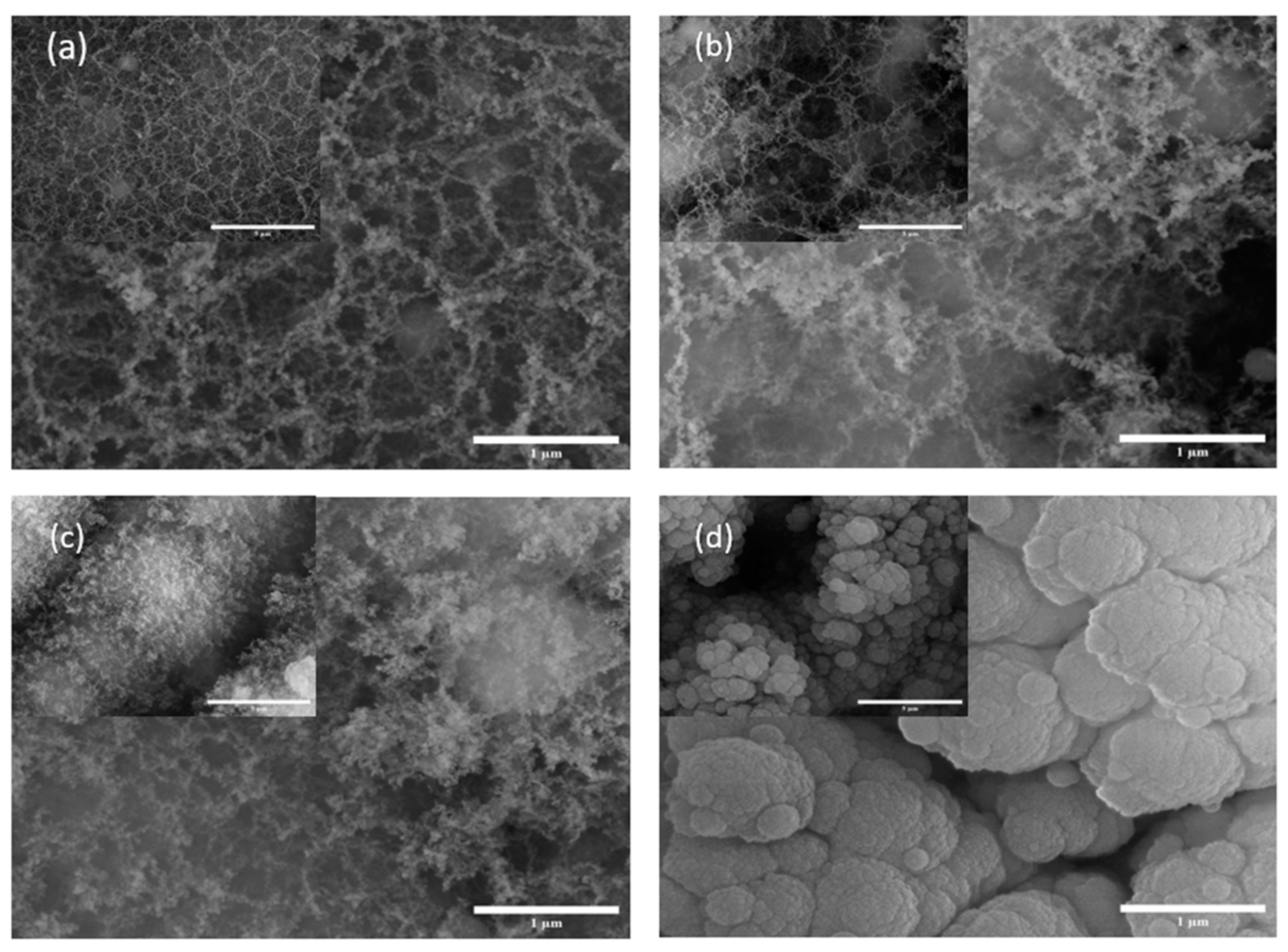
The SEM done on the samples are illustrated in Figure 1 and Figure 2. With the SEM images in Figure 1, it is evident that there is a higher fiber generation in Si1 compared with the others. Additionally, we can see that the nanostructures in Si2 and Si3 are quite similar and have a similar texture; the difference between the two is a that thicker or more agglomerated structures as can be at the 1 mm scale. Figure 1d shows the Si4 sample which has a more agglomerated structure and fibers are hardly visible. Here, the fibers have agglomerated due to ablation. Thus, a shorter pulse duration in the picosecond range offers ambient ablation and allows the samples to cool down during the process and, in turn, decreases the surface temperature.

Figure 1.
SEM images of silicon wafer samples at 500× (inset) and 35,000× magnifications: (a) Si1, (b) Si2, (c) Si3 and (d) Si4.

Figure 2.
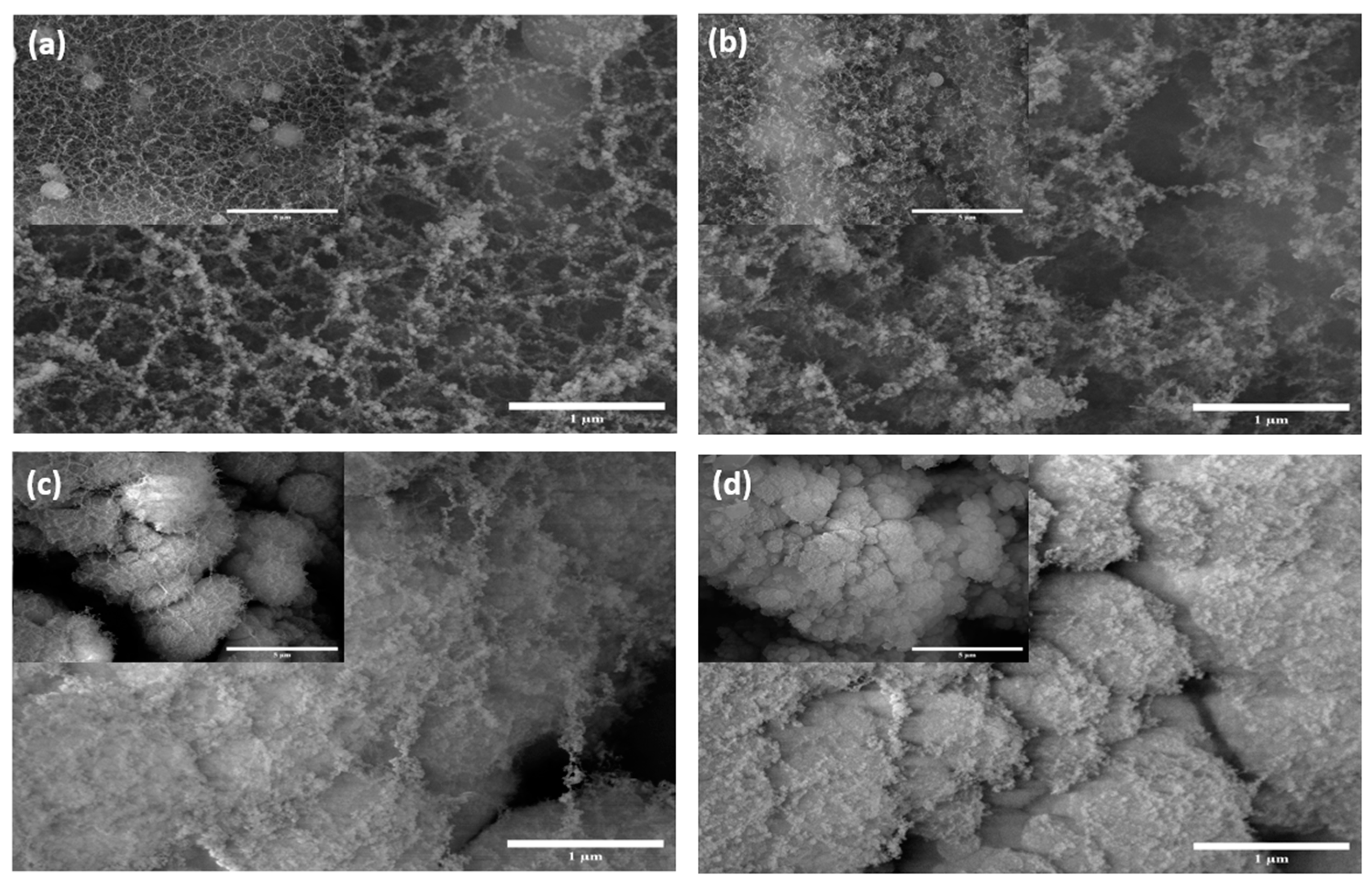
SEM images of gold-coated silicon wafer samples at500× (inset) and 35,000× magnifications: (a) AuSi1, (b) AuSi2, (c) AuSi3 and (d) AuSi4.
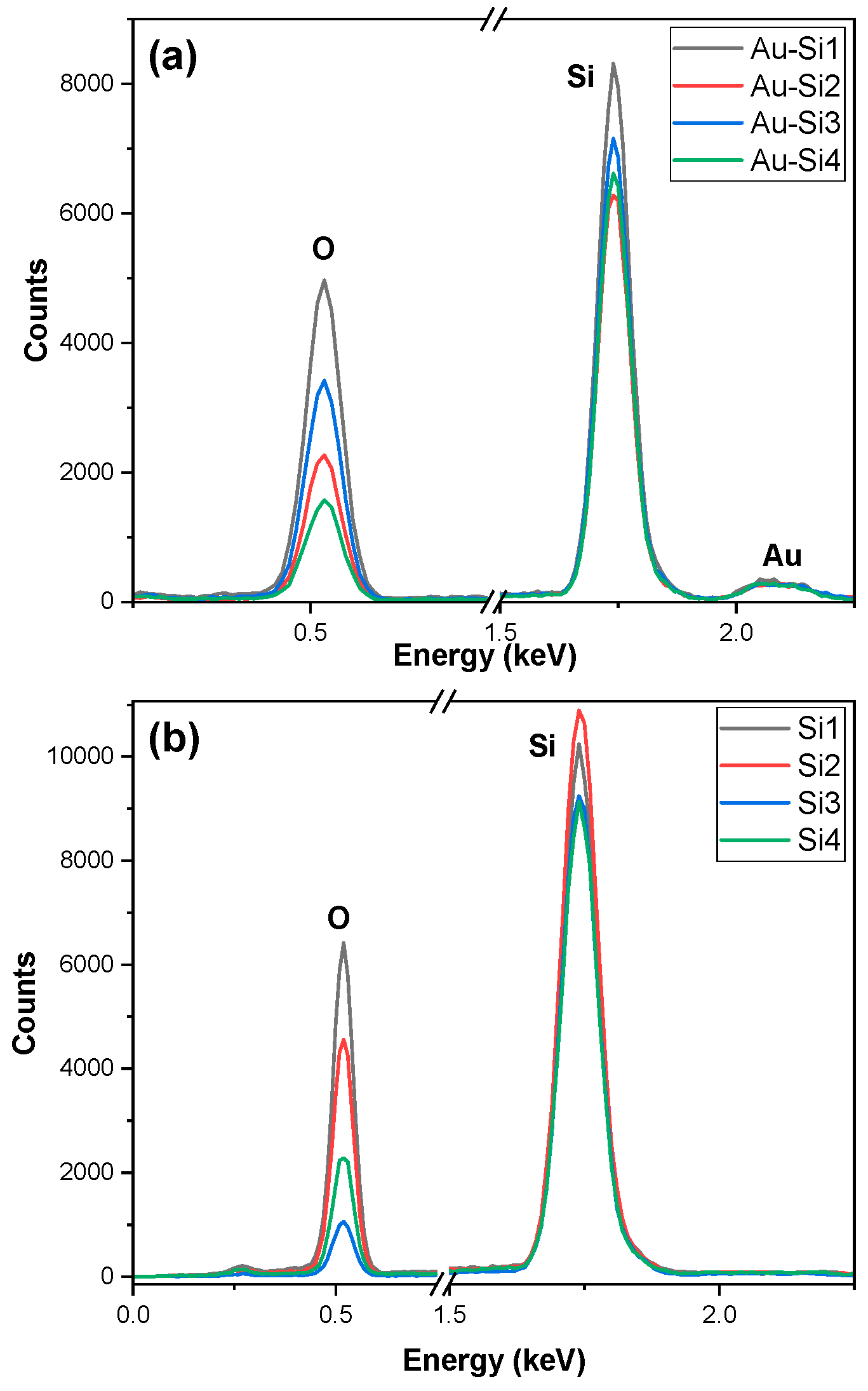
In the EDX graph for the sample in Figure 3b, we observed a higher oxidation for the Si1 sample. The oxidation was lower for Si3 than Si4; however, the structure in Si3 was better and more refined. This was a result of the pulse duration being higher, due to which the burst of light was higher for a longer period. The ablated particles did not have enough time for the dissipation of heat from ablation. The formed particles were agglomerated [16].
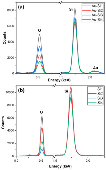
Figure 3.
EDX of the samples: (a) gold-coated silicon and (b) silicon.
Figure 2 shows the SEM images for the gold-coated samples. The nano-structuring on these samples shows a similar trend to that of silicon wafer and the reasons are also similar. The pulse duration of the laser is indeed an important parameter to determine the structure formation for the samples using ULPING. The structures in the samples are denser and more nanostructures are visible. It is suspected that these nanostructures are of gold.
The presence of gold can be confirmed by the EDX graphs which are given in Figure 3a There is a small peak of gold, which indicates that gold is present in the samples and the amount is lower. The amount of gold was almost similar for all the samples despite being ablated. The weight percentage was between 6 and 11% for the samples. The oxidation was higher for the Au-Si1 sample and decreased for the other samples. It was almost similar for the Au-Si2 and Au-Si3 samples. A higher oxidation confirms that more silicon oxide is formed on the samples.
4.2. XPS
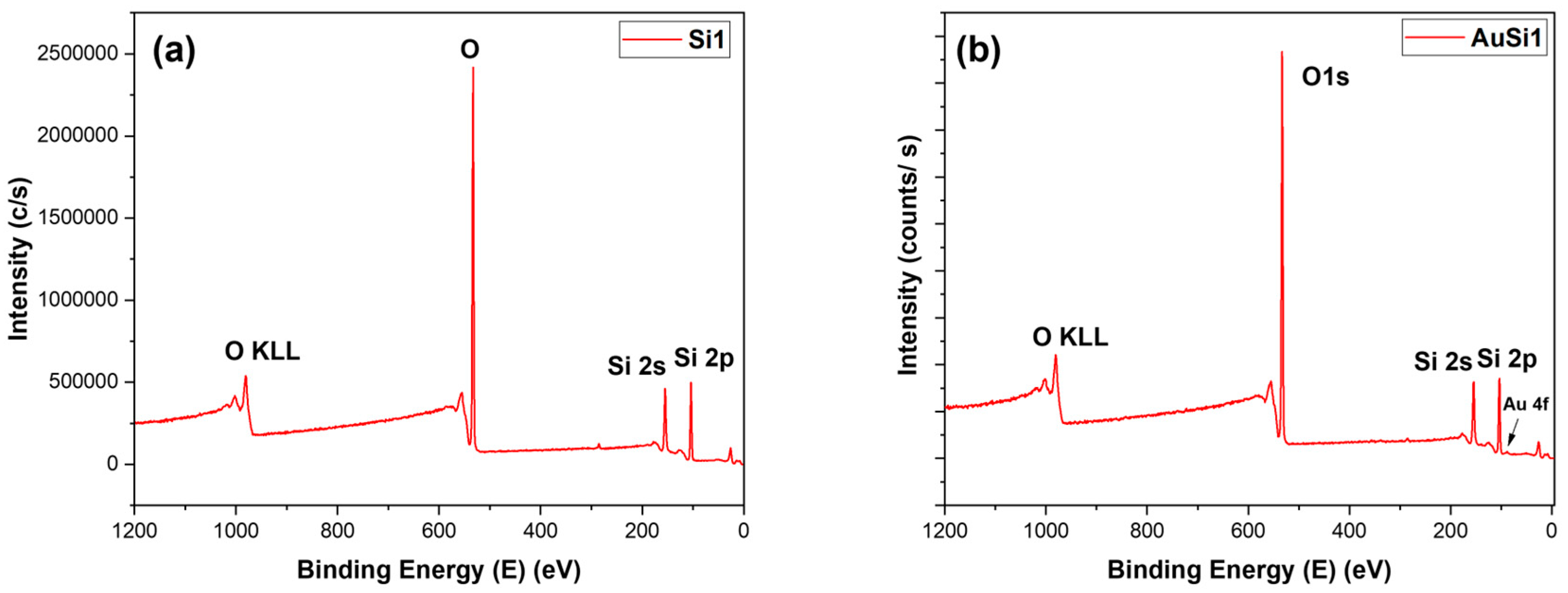
It was important to perform XPS on the samples to determine the constituents on the thin layer synthesized on the samples. From the peaks of the samples and based on the type of the material, the certainty of the bonds can be clarified from EDX. The XPS graphs are quite alike for all samples and can be easily comprehended. The XPS surveys are illustrated in Figure 4, where the only difference is a small gold 4f peak. The peak is comparatively very small compared to the other peaks, as the amount of gold decreased with laser ablation.
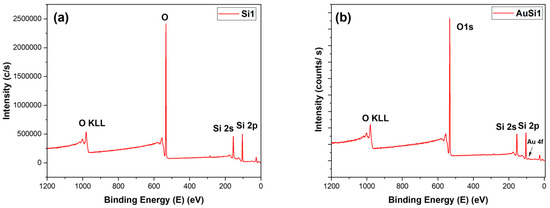
Figure 4.
XPS survey: (a) Si1 and (b) AuSi1.
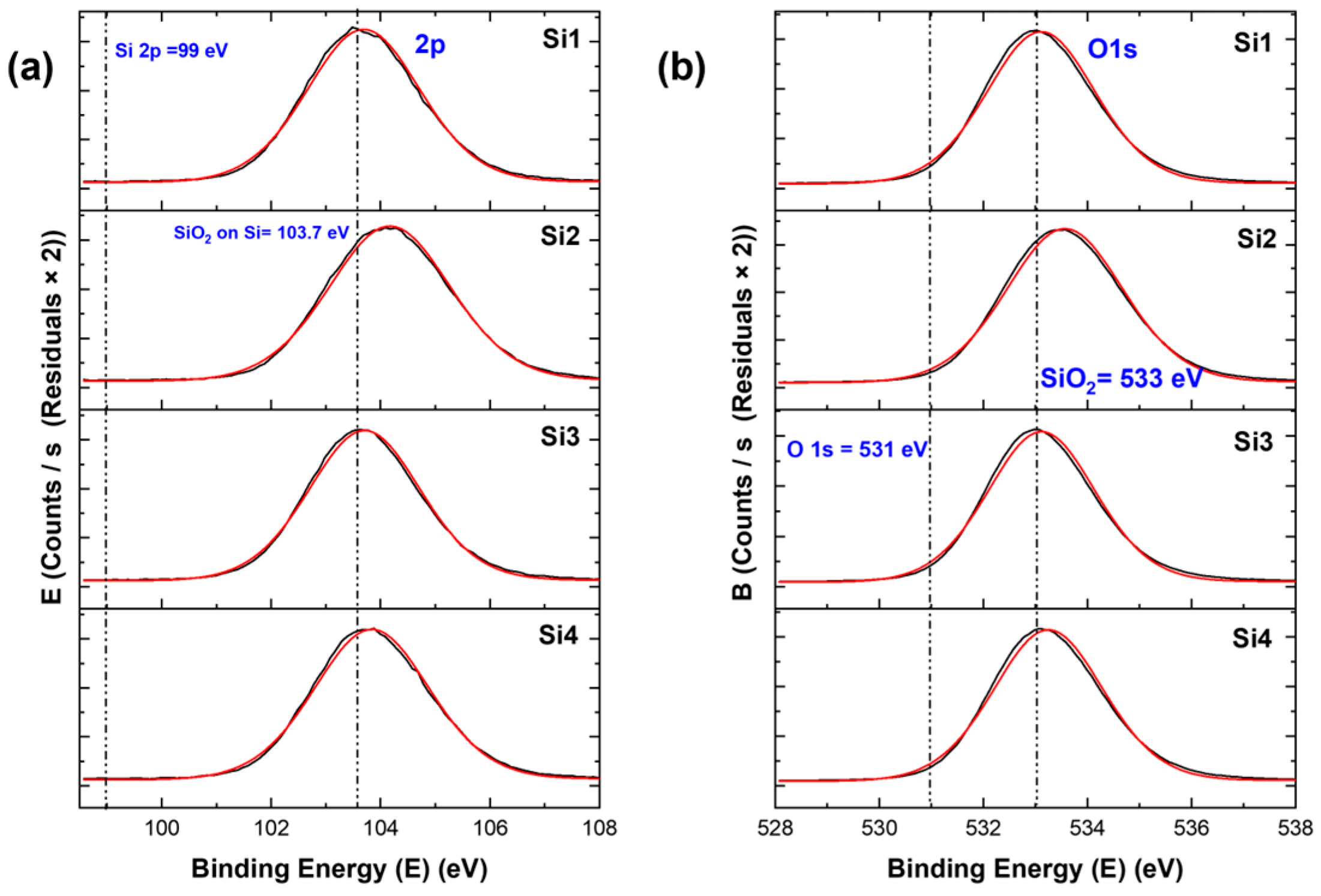
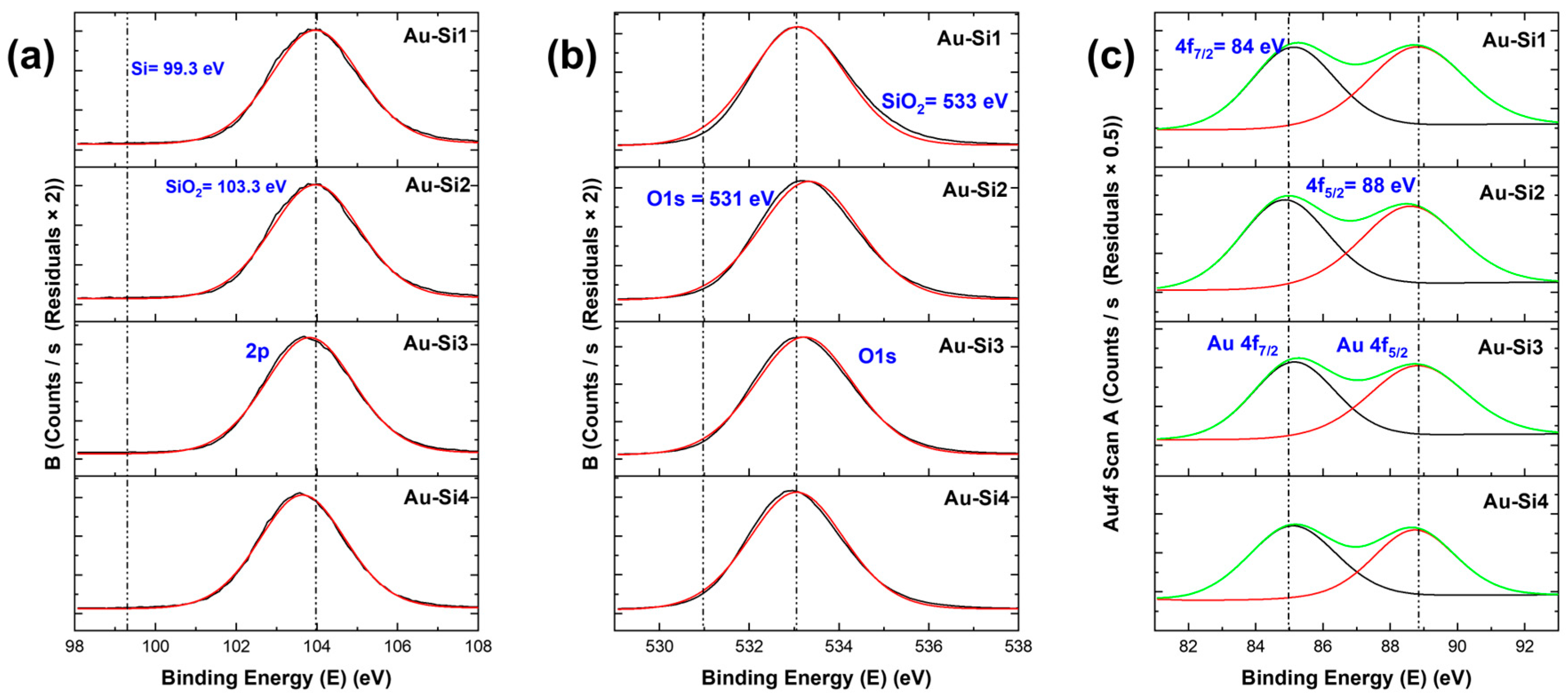
For the samples, when we see the specific higher resolution XPS peaks, we observed chemical shifts for all samples. These chemical shifts are important as they determine the type of compound formed. For the Si 2p peak in Figure 5 and Figure 6, for both types of materials, a shift of the peak from binding energies 99 eV to 103–104 eV can be seen. The former (99 eV) specifies the Si–Si bond [17], the latter specifies the SiO2 in Si. This was similar in the case of the O 1s peak, where a shift from 531 eV to around 533 eV was observed, corresponding to O2 in silicon oxide [17]. These Si 2p and O 1s peaks indicate that all samples had a higher surface oxidation, which led to the formation of silicon oxide. The atomic ratios indicated that the samples with higher nanostructures had higher Si/SiO2 ratios. For the Au 4f peak, we can see two peaks (Figure 6c). The 4f7/2 is the higher one, which corresponds to gold. There is no shift in the gold peaks; thus, this means that gold did not form new bonds or compounds. The atomic ratio of gold is quite low for the samples when compared to Si and O.
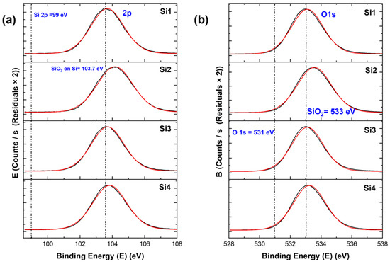
Figure 5.
XPS peaks for silicon samples: (a) Si 2p peaks and (b) O 1s peaks. Here, the black curve is the XPS curve and the red curve is the envelope.
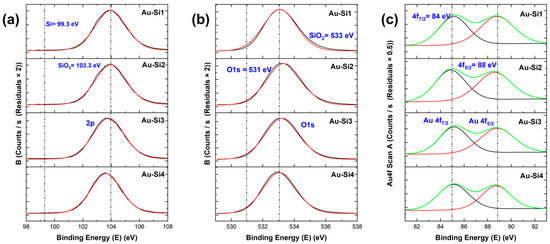
Figure 6.
XPS peaks of Au-coated silicon samples: (a) Si 2p peaks, (b) O 1s peaks and (c) Au 4f peaks (the green curve is the main peak and black and green peaks are the satellite peaks).
5. Optical Properties
5.1. Band Gap
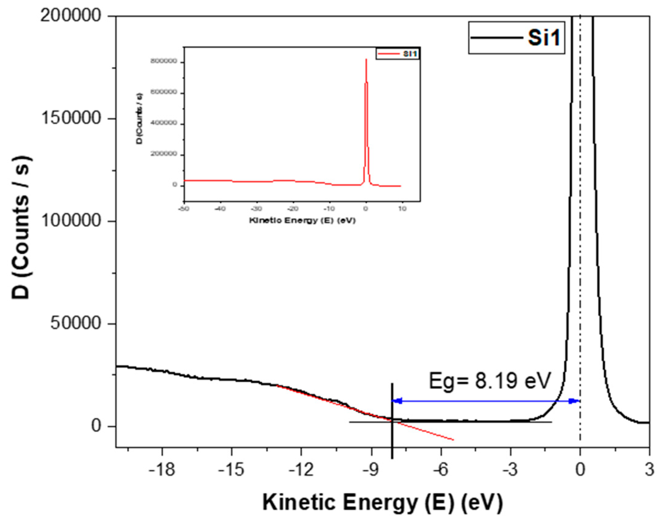
The band gap is an important parameter which determines the conductivity of the samples. Here, the band gap was measured using REELS. As the thin film deposited is silicon oxide, REELS measured just the top layer. Based on REELS, the band gaps were determined using the loss energy peak [18,19], as shown in Figure 7. The values for the band gaps for both sets of samples were between 7.5 eV and 8.2 eV.
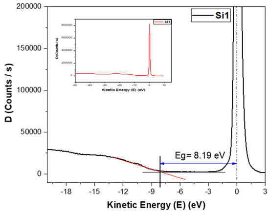
Figure 7.
Determination of band gap from the energy loss peak of REELS spectra of the Si1 sample. The inset figure shows the larger scale spectroscopy results.
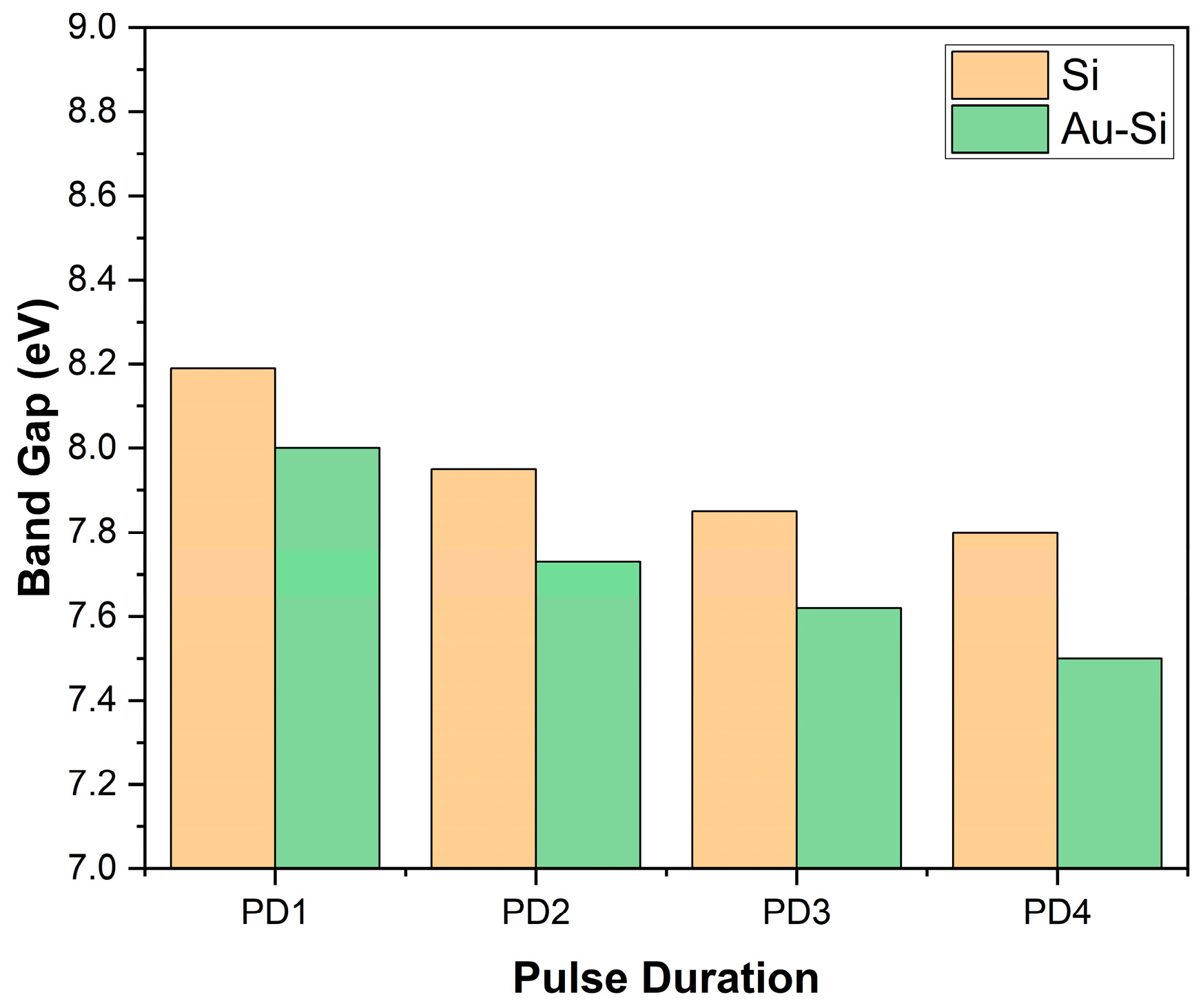
Figure 8 illustrates the bar graph depicting the band gaps of the samples based on the pulse duration of the laser source. Here, it can be observed that as the pulse duration increased, the band gap of the samples decreased. In other words, the samples with higher nanostructures had a higher band gap value.
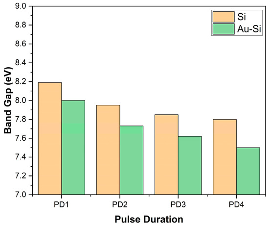
Figure 8.
Band gap of the samples using REELS.
Additionally, the samples with a gold coating had a lower band gap than the samples on bare silicon wafer using the same parameters. The addition of gold reduced the band gap of the layer.
5.2. Band Offset
The formed layers are a composite of silicon, silicon oxide and embedded gold in the case of gold-coated samples. In this case, the band offset should be determined. In order to determine the offset, we initially had to find the band edges for the valence and conduction bands of the materials.
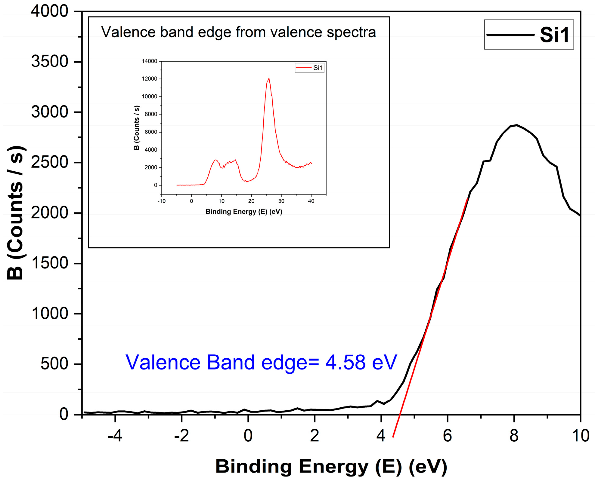
The valence band edge or valence band minimum was found using the valence band spectra from XPS [20,21], as shown in Figure 9. The band gap was found from REELS, as discussed previously. Using the two, the conduction band was found.
Valence band maximum (VBM) − conduction band minimum (CBM) = Band gap
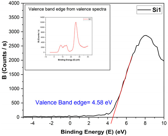
Figure 9.
Determination of the valence band edge from valence spectra for the Si1 sample. Inst image shows the full spectroscopy range collected from the sample.
The band offsets were determined using Kraut’s Method [22], where the valence band offset (VBO) [23],
For the conduction band offset,
The band gap of the reference silicon sample was 1.12 eV and for the gold-coated silicon, it was determined to be 0.5 eV using REELS. These values are tabulated (Table 2), and this offset is illustrated using Figure 10.

Table 2.
Band gap and band offsets of the samples.
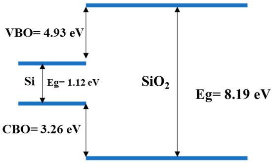
Figure 10.
Illustration of the band offset for the Si1 sample.
The band offset is quite similar for all the samples; however, we noticed a higher valence band offset for the samples on bare silicon. The embedded gold particles also reduced the band gap, thus, reducing the band edges. The band edges were present as the amount if gold was very low and the nanoparticles allowed for the creation of discrete energy bands. Here, the samples with higher nanostructures had a better offset as well.
5.3. Optical Conductivity
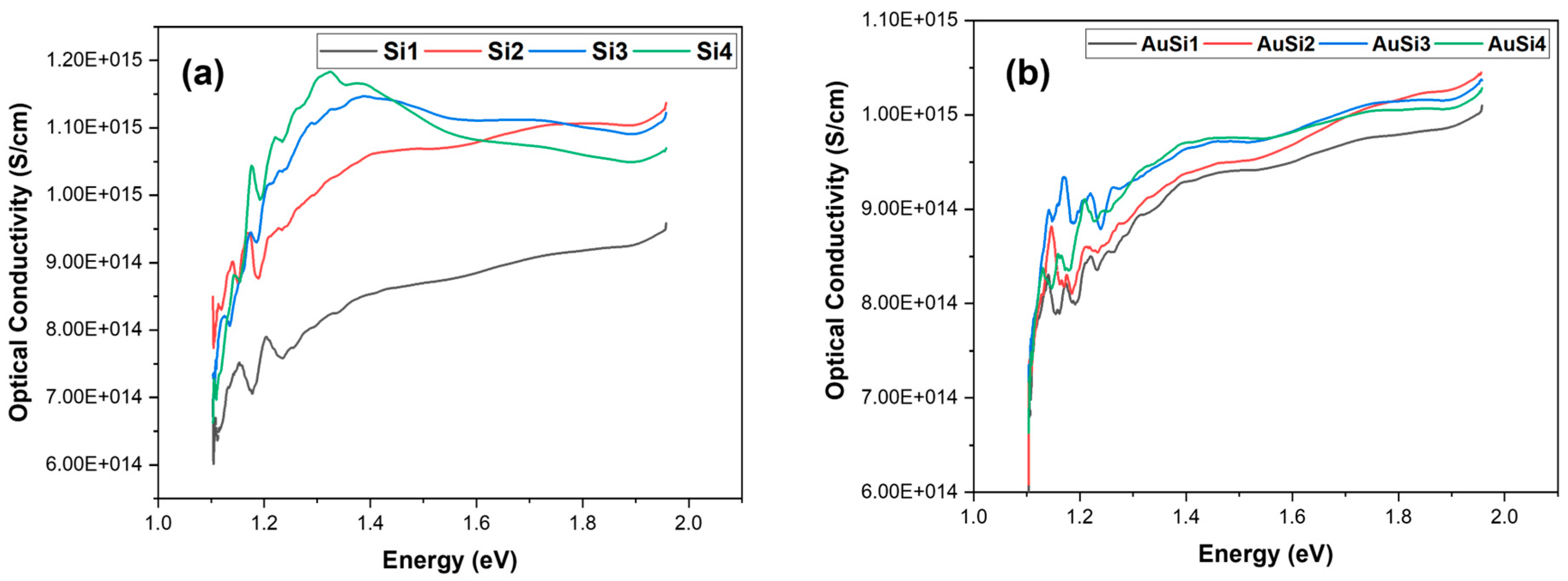
Optical spectroscopy was performed on the samples to determine the optical conductivity. The optical conductivity of the samples helps in determining how much energy would be required for the material to conduct light. The optical conductivity of a material is inversely proportional to the band gap; the higher the band gap, the lower the optical conductivity. It is proportional to the absorption co-efficient of the sample.
The equation to determine optical conductivity is
where α is the absorption co-efficient of the material. The Kubelka–Munk equation was used here to determine the absorption co-efficient. The Kubelka–Munk function F(R) is equivalent to the absorption co-efficient and, similarly, the refractive index is determined from the same function [24].
From Figure 11, it is evident that the optical conductivity is lower for the samples that have a higher band gap. The optical conductivity is comparatively higher for gold-coated samples. Gold plays an important role in creating contact pads on the silicon surface; this is due to its tendency of not oxidizing and it is also resistant to electromigration. The addition of gold increases the absorption of photon energy and, thus, increases the optical conductivity of the material, in turn decreasing the band gap of the material. For the silicon samples, the conductivity decreases at higher wavelengths and as the wavelength decreases, we observe a steady rise in the optical conductivity of the samples. The sample with a lower nanostructure formation (Si3, Si4) shows a steady decline in the optical conductivity at lower wavelengths or higher photon energies. This is because silicon is transparent for the UV range [25]. However, as the nanostructures are formed, a blue shift is observed where the decline of optical conductivity is not observed [26]. This change is not major for nanoparticles. The same was observed for the gold-coated samples as well, although, due to the presence of gold, the samples showed an increase in conductivity at higher photon energy [27].
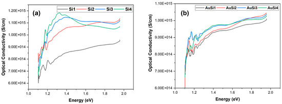
Figure 11.
Optical conductivity of the samples: (a) silicon and (b) gold-coated silicon.
6. Conclusions
Ultra-short laser pulses for in situ nanostructure generation (ULPING) were employed for the synthesis of hybrid nanostructures with tuned optical properties from silicon and gold-coated silicon samples. The effects of varying pulse duration of the laser source on the nanostructure formation were analyzed, and it was found that fiber generation was higher at a shorter pulse duration. This was common for both types of materials. An agglomeration was observed at a higher pulse duration which was due to a higher surface temperature and higher ablation. The samples with higher nanostructures had a higher band gap and band offset, with the highest being 8.19 eV for the Si1 sample. The addition of gold decreased the band gap of the material and increased the optical conductivity of the samples. The optical conductivity had a reverse trend to that of the band gap and a blue shift was noticed for the silicon samples where nanofibers were generated. The results of this project can lead to promising solutions for fabrication of nanomaterials with tuned optoelectrical properties for photonics, nanoelectronics and solar energy applications.
Author Contributions
N.S.J.: methodology, visualization, investigation, software, data collection and data analysis, writing—original draft preparation, writing—reviewing and editing. A.K.: conceptualization, supervision, methodology, investigation, software, validation, data curation, writing—reviewing and editing. All authors have read and agreed to the published version of the manuscript.
Funding
The authors acknowledge the support of the Natural Sciences and Engineering Research Council of Canada (NSERC), grant number RGPIN-2022-03992.
Institutional Review Board Statement
Not applicable.
Informed Consent Statement
Not applicable.
Data Availability Statement
The data can be provided upon request.
Acknowledgments
This research was partially supported by the Natural Sciences and Engineering Research Council of Canada (NSERC).
Conflicts of Interest
The authors declare no conflict of interest.
References
- Newman, C.; Chesterfield, R.; Merlo, J.; Frisbie, C.D. Transport properties of single-crystal tetracene field-effect transistors with silicon dioxide gate dielectric. Appl. Phys. Lett. 2004, 85, 422–424. [Google Scholar] [CrossRef]
- Choi, W.Y.; Lee, W. Hetero-gate-dielectric tunneling field-effect transistors. IEEE Trans. Electron Devices 2010, 57, 2317–2319. [Google Scholar] [CrossRef]
- Ortiz, R.; Facchetti, A.; Marks, T. High-k organic, inorganic, and hybrid dielectrics for low-voltage organic field-effect transistors. Chem. Rev. 2010, 110, 205–239. [Google Scholar] [CrossRef] [PubMed]
- Meijer, E.; Gelinck, G.; Van Veenendaal, E.; Huisman, B.-H.; De Leeuw, D.; Klapwijk, T. Scaling behavior and parasitic series resistance in disordered organic field-effect transistors. Appl. Phys. Lett. 2003, 82, 4576–4578. [Google Scholar] [CrossRef]
- Tseng, C.-W.; Tao, Y.-T. Electric bistability in pentacene film-based transistor embedding gold nanoparticles. J. Am. Chem. Soc. 2009, 131, 12441–12450. [Google Scholar] [CrossRef] [PubMed]
- Sant, S.; Schenk, A. Band-offset engineering for GeSn-SiGeSn hetero tunnel FETs and the role of strain. IEEE J. Electron Devices Soc. 2015, 3, 164–175. [Google Scholar] [CrossRef]
- Casperson, J.D.; Bell, L.; Atwater, H.A. Materials issues for layered tunnel barrier structures. J. Appl. Phys. 2002, 92, 261–267. [Google Scholar] [CrossRef]
- Gago, R.; Vázquez, L.; Cuerno, R.; Varela, M.; Ballesteros, C.; Albella, J.M. Production of ordered silicon nanocrystals by low-energy ion sputtering. Appl. Phys. Lett. 2001, 78, 3316–3318. [Google Scholar] [CrossRef]
- Li, F.J.; Zhang, S.; Kong, J.; Zhang, W.L. Study of silicon dioxide nanowires grown via rapid thermal annealing of sputtered amorphous carbon films doped with Si. Nanosci. Nanotechnol. Lett. 2011, 3, 240–245. [Google Scholar] [CrossRef]
- Suk, J.-H.; Hong, S.-C.; Jang, G.-S.; Hwang, N.-M. Two-step deposition of silicon oxide films using the gas phase generation of nanoparticles in the chemical vapor deposition process. Coatings 2021, 11, 365. [Google Scholar] [CrossRef]
- Chen, X.Y.; Lu, Y.F.; Tang, L.J.; Wu, Y.H.; Cho, B.J.; Xu, X.J.; Dong, J.R.; Song, W.D. Annealing and oxidation of silicon oxide films prepared by plasma-enhanced chemical vapor deposition. J. Appl. Phys. 2005, 97, 014913. [Google Scholar] [CrossRef]
- Chen, T.; Wang, W.; Tao, T.; Pan, A.; Mei, X. Multi-scale micro-nano structures prepared by laser cleaning assisted laser ablation for broadband ultralow reflectivity silicon surfaces in ambient air. Appl. Surf. Sci. 2020, 509, 145182. [Google Scholar] [CrossRef]
- Jia, X.; Li, Z.; Wang, C.; Li, K.; Zhang, L. Study of the dynamics of material removal processes in combined pulse laser drilling of alumina ceramic. Opt. Laser Technol. 2023, 160, 109053. [Google Scholar] [CrossRef]
- Jia, X.; Chen, Y.; Liu, L.; Wang, C. Combined pulse laser: Reliable tool for high-quality, high-efficiency material processing. Opt. Laser Technol. 2022, 153, 108209. [Google Scholar] [CrossRef]
- Ding, K.; Wang, C.; Li, S.; Zhang, X.; Lin, N. Large-area cactus-like micro-/nanostructures with anti-reflection and superhydrophobicity fabricated by femtosecond laser and thermal treatment. Surf. Interfaces 2022, 33, 102292. [Google Scholar] [CrossRef]
- Serkov, A.; Shcherbina, M.; Kuzmin, P.; Kirichenko, N. Laser-induced agglomeration of gold nanoparticles dispersed in a liquid. Appl. Surf. Sci. 2015, 336, 96–102. [Google Scholar] [CrossRef]
- Alfonsetti, R.; Lozzi, L.; Passacantando, M.; Picozzi, P.; Santucci, S. XPS studies on SiOx thin films. Appl. Surf. Sci. 1993, 70, 222–225. [Google Scholar] [CrossRef]
- Heo, S.; Cho, E.; Lee, H.-I.; Park, G.S.; Kang, H.J.; Nagatomi, T.; Choi, P.; Choi, B.-D. Band gap and defect states of MgO thin films investigated using reflection electron energy loss spectroscopy. AIP Adv. 2015, 5, 077167. [Google Scholar] [CrossRef]
- Vos, M.; King, S.; French, B.L. Measurement of the band gap by reflection electron energy loss spectroscopy. J. Electron Spectrosc. Relat. Phenom. 2016, 212, 74–80. [Google Scholar] [CrossRef]
- Zatsepin, D.; Mack, P.; Wright, A.; Schmidt, B.; Fitting, H.J. XPS analysis and valence band structure of a low-dimensional SiO2/Si system after Si+ ion implantation. Phys. Status Solidi A 2011, 208, 1658–1661. [Google Scholar] [CrossRef]
- Fares, C.; Tadjer, M.J.; Woodward, J.; Nepal, N.; Mastro, M.A.; Eddy, C.R.; Ren, F.; Pearton, S.J. Valence and conduction band offsets for InN and III-nitride ternary alloys on (−201) bulk β-Ga2O3. ECS J. Solid State Sci. Technol. 2019, 8, Q3154. [Google Scholar] [CrossRef]
- Jung, D.; Jang, Y.; Sultane, P.; Bielawski, C.; Oh, J. Energy band offsets of BeO dielectrics grown via atomic-layer deposition on β-Ga2O3 substrates. J. Alloys Compd. 2022, 922, 166197. [Google Scholar] [CrossRef]
- Zhu, Y.; Jain, N.; Hudait, M.; Maurya, D.; Varghese, R.; Priya, S. X-ray photoelectron spectroscopy analysis and band offset determination of CeO2 deposited on epitaxial (100),(110), and (111) Ge. J. Vac. Sci. Technol. B Nanotechnol. Microelectron. Mater. Process. Meas. Phenom. 2014, 32, 011217. [Google Scholar]
- Jamwal, N.S.; Kiani, A. Synthesis of 3D Nanonetwork Si Structures via Direct Ultrafast Pulsed Nanostructure Formation Technique. Energies 2022, 15, 6005. [Google Scholar] [CrossRef]
- Jakšić, Z.; Maksimović, M.; Sarajlić, M. Silver–silica transparent metal structures as bandpass filters for the ultraviolet range. J. Opt. A Pure Appl. Opt. 2004, 7, 51. [Google Scholar] [CrossRef]
- Tsunekawa, S.; Fukuda, T.; Kasuya, A. Blue shift in ultraviolet absorption spectra of monodisperse CeO2−x nanoparticles. J. Appl. Phys. 2000, 87, 1318–1321. [Google Scholar] [CrossRef]
- Zhu, Y.; Li, Z.; Hao, Z.; DiMarco, C.; Maturavongsadit, P.; Hao, Y.; Lu, M.; Stein, A.; Wang, Q.; Hone, J.; et al. Optical conductivity-based ultrasensitive mid-infrared biosensing on a hybrid metasurface. Light Sci. Appl. 2018, 7, 67. [Google Scholar] [CrossRef]
Disclaimer/Publisher’s Note: The statements, opinions and data contained in all publications are solely those of the individual author(s) and contributor(s) and not of MDPI and/or the editor(s). MDPI and/or the editor(s) disclaim responsibility for any injury to people or property resulting from any ideas, methods, instructions or products referred to in the content. |
© 2023 by the authors. Licensee MDPI, Basel, Switzerland. This article is an open access article distributed under the terms and conditions of the Creative Commons Attribution (CC BY) license (https://creativecommons.org/licenses/by/4.0/).

