Article

Optical Characterization of Gadolinium Fluoride Films Using Universal Dispersion Model

1
Department of Physical Electronics, Faculty of Science, Masaryk University, Kotlářská 2, 611 37 Brno, Czechia
2
Czech Metrology Institute, Okružní 31, 638 00 Brno, Czechia
3
Meopta-Optika, s.r.o., Kabelíkova 1, 750 02 Přerov, Czechia
*
Author to whom correspondence should be addressed.
Coatings 2023, 13(2), 218; https://doi.org/10.3390/coatings13020218
Submission received: 16 December 2022 / Revised: 9 January 2023 / Accepted: 13 January 2023 / Published: 17 January 2023
(This article belongs to the Special Issue Optical Thin Films: Preparation, Application and Development)

Abstract

:
The optical characterization of gadolinium fluoride (GdF3) films is performed in a wide spectral range using heterogeneous data-processing methods (the ellipsometric and spectrophotometric measurements for five samples with thicknesses ranging from 20 to 600 nm are processed simultaneously). The main result of the characterization is the optical constants of GdF3 in the range from far infrared to vacuum ultraviolet, both in the form of a table and in the form of dispersion parameters of the universal dispersion model (UDM). Such reliable data in such a broad spectral range have not been published so far. The GdF3 films exhibit several defects related to the porous polycrystalline structure, namely, surface roughness and a refractive index profile, which complicate the optical characterization. The main complication arises from the volatile adsorbed components, which can partially fill the pores. The presented optical method is based on the application of the UDM for the description of the optical response of GdF3 films with partially filled pores. Using this dispersion model, it is possible to effectively separate the optical response of the host material from the response of the adsorbed components. Several recently published structural and dispersion models are used for optical characterization for the first time. For example, a model of inhomogeneous rough films based on Rayleigh–Rice theory or asymmetric peak approximation with a Voigt profile for the phonon spectra of polycrystalline materials.

1. Introduction

The universal dispersion model (UDM) describes individual elementary electronic and phonon excitations in materials as separate contributions [1]. This dispersion model satisfies three fundamental conditions: time reversal symmetry, Kramers–Kronig consistency and conformity with the sum rules. The UDM is a suitable dispersion model for a very precise description of the response function of optical materials in a wide spectral range [2,3,4,5,6,7].
Optical materials used in thin-film interference optics often have a polycrystalline structure [8,9,10,11]. For optical purposes, it is necessary to prepare polycrystalline thin films with a very fine structure, where the mean size of the grains is much smaller than the wavelength of light for which the system is designed. However, this is difficult to achieve in practice. The size of the grains accompanied by surface roughness is sensitive to deposition conditions and often changes during the growth [12,13,14]. In the first phase of deposition, polycrystalline material with very fine grains grows. The size of the grains then gradually increases with the thickness of the film, until the film becomes optically unusable. The internal scattering in the film (extinction) increases with the size of the grains and the scattering losses at the interfaces also increase due to the roughness [15,16]. In addition, films with large grains show a porosity that negatively affects the extinction coefficient in the transparent region due to the presence of localized states [17,18,19]. The localized states originate in the surface states of the grains as well as in the adsorbed substances in the pores, which constitute unstable components depending on the environmental conditions. All these defects negatively affect the properties of the films and layered systems containing these films. This is why only limited work has been performed so far and the optical constants of many fluoride films are thus known only in the transparent region with large uncertainty [20].
This article will focus on GdF3 material that is used as a high-index material for multilayer coatings in the UV region due to its high band-gap energy. It will be shown that GdF3 films exhibit the defects mentioned above and that the UDM is an effective tool by which to describe the optical properties of these films.

2. Sample Preparation

GdF3 single films were prepared by thermal evaporation with a SYRUSpro 1110 coating plant in DUV configuration onto the weakly doped float zone single-crystal silicon substrates (B-doped 5 × 10 13 cm 3 , resistivity 80 Ω cm , orientation (100)). The coater chamber was pumped down to a base pressure lower than 2.0 × 10 6   m and heated up to 300 °C for 1 hour before deposition. The substrates were treated using oxygen plasma with a built-in advanced plasma source (APS) for 3 min. After that, GdF3 films were deposited in nominal thicknesses of 20 nm, 100 nm, 200 nm, 300 nm and 600 nm with a deposition rate of 0.5 nm s−1. The film thickness during the growth was monitored using the quartz crystal microbalance (QCM) method.

3. Experimental Arrangement

Experimental data were acquired using two ellipsometers and three spectrophotometers: Woollam IR-VASE, Horiba Jobin Yvon UVISEL, Bruker Vertex 80v, Perkin Elmer Lambda 1050 and McPherson VUVAS 1000. These data covered a wide spectral range of 0.00868–10.3 eV (70–83,300 cm 1 ; 0.12–143 μ m ). The measurements obtained using individual instruments in individual spectral ranges resulted in 16 data sets for each sample. Thus, a total of 80 experimental data sets were used in the optical characterization (for further details see the Supplementary Materials).
The ellipsometry was represented by the vector of associated ellipsometric parameters ( I s , I c , I n ) [21]. The associated ellipsometric parameters correspond to the three independent elements of the normalized Mueller matrix of isotropic systems:
M = R 1 I n 0 0 I n 1 0 0 0 0 I c I s 0 0 I s I c ,
where R is the average reflectance (T instead of R appears for the transmitted light). Ellipsometric data were measured from both sides of the sample in the infrared region, where the substrate is transparent. The difference ellipsometry data
( Δ I s , Δ I c , Δ I n ) = ( I s , I c , I n ) f ( I s , I c , I n ) b ,
were used in addition to the ellipsometric data ( I s , I c , I n ) f measured from the side with the GdF3 film (front side) and the data ( I s , I c , I n ) b measured from the opposite side (back side). Although these data are not independent, the inclusion of difference ellipsometry in the data processing helps to reduce the influence of the substrate and systematic errors [2,5]. In the UV and VIS spectral range, where the silicon substrate is not transparent, the ellipsometry was also measured from the back side in order to determine the thickness of the native oxide layer. For this purpose it was sufficient to make measurements for a relatively small number of spectral points at one angle of incidence.
As for spectrophotometry, both absolute quantities (reflectance and transmittance) and relative reflectance were processed. The relative reflectance was calculated as the ratio of the reflectance R f from the front side and the reflectance R b from the back side of the sample:
R r = R f R b .
According to our experience, similar to difference ellipsometry, the relative reflectance helps to reduce the correlations between the sought parameters by compensating for systematic errors in measurement [2,5].

4. Data Processing

The essential tool for reducing the systematic errors and increasing the reliability of the obtained results is that we combined different data from different instruments measured on several samples with films differing in thickness. The simultaneous processing of these data constitute a heterogeneous data processing method combining multi-data, multi-instrument and multi-sample methods.
Data processing was performed using newAD2 software [22] supporting parallel calculations distributed by pvm (parallel virtual machine) libraries [23]. This software allowed us to perform unique heterogeneous data processing [7] using the least-squares method with the Levenberg–Marquardt algorithm (LMA) [24,25]. The modified version of the LMA enabled us to automatically equalize the contributions of individual experimental data sets to the residual sum of squares [2,5,7], which is crucial for heterogeneous data processing.

5. Structural Model of Samples

The samples consisted of double-sided polished silicon single-crystal substrates with the GdF3 films deposited on one side (see Figure 1). Since the substrates were exposed to air, it was assumed that the back sides were covered by thin native oxide layers (NOLs), which were modeled as thin homogeneous films with thickness d nol . Since no special effort was made to remove the NOLs from the surfaces of the silicon substrates before the deposition of the films, it is possible that parts of the NOLs remained below the GdF3 films. Moreover, the treating of substrates by the oxygen plasma prior to the deposition of the films could also be a contributing factor to the NOLs. In the structural model, this is represented by transition layers between the GdF3 films and the silicon substrates, which were modeled as thin homogeneous films with thickness d t and with optical constants identical to the NOLs. The optical constants of float-zone silicon substrates and the NOLs were modeled by UDM with parameters fixed in values corresponding to our previous study of crystalline silicon wafers [6,26] (for optical constants see the Supplementary Materials). In general, the optical response of the NOLs is similar to amorphous SiO 2 . The exact values of the refractive index play only a minor role because of the correlation with the NOL thickness.
The GdF3 films with nominal thickness above 20 nm were modeled using inhomogeneous films with randomly rough upper boundaries (see Figure 1). Since the films were deposited on the polished substrate, it was assumed that the lower boundaries of the GdF3 films as well as the boundaries of the transition layers were smooth. In the structural model, the inhomogeneous film with thickness d f is approximated by a stack of m + 1 thin homogeneous films. The mean thicknesses of the films in this stack are equal to d f / m with the exception of the first and last films, which have a mean thickness d f / ( 2 m ) . The value of m was chosen differently for each film such that the ratio of nominal thickness and m was 20 nm. The thinnest films with nominal thickness 20 nm were assumed to be homogeneous. Moreover, because it was found that the roughness of the thinnest films was very small (see Section 7, Table 1), they were not considered in the structural model.
The optical constants n ^ j of the films in the stack were chosen as
n ^ j = ε ^ ( z j ) , where z j = j m d f ,
where the index j = 0 , 1 , , m numbers the films and ε ^ ( z ) represents dependence of the dielectric function on the coordinate z perpendicular to the surface of the substrate. The arrangement with the first and last films in the stack having half the thickness of the other films is advantageous, since the convergence to the exact result corresponding to the films with a continuous profile of the optical constants (i.e., to the limit m ) is faster than if all the films had the same thickness [27]. All the boundaries in this stack were assumed to be rough, except for the boundary at z = 0 , which separates the GdF3 film from the transition layer. The irregularities in the roughness were identical in shape, but their heights were scaled proportionally to the distance of the mean planes from the boundary at z = 0 . Therefore the root-mean-square (RMS) value of the heights of irregularities of the j-th boundary is
σ j = z ¯ j d f σ , z ¯ j = 0 for j = 0 , 2 j 1 2 m d f for j = 1 , 2 , , m , d f for j = m + 1 ,
where z ¯ j denotes the positions of the mean planes and the value σ corresponds to the roughness on the surface of the GdF3 film.
The Fresnel coefficients of the layered systems with randomly rough boundaries were calculated using the Rayleigh–Rice theory (RRT). The reflection coefficients are expressed as
r ^ α = r ^ α [ 0 ] + r ^ α [ 2 ] ,
where α = p , s distinguishes the p and s polarized waves, the symbol r ^ α [ 0 ] denotes the reflection coefficient calculated as if all the boundaries were smooth and the symbol r ^ α [ 2 ] represents the correction calculated using the RRT. It can be written in the following form [28,29]
r ^ α [ 2 ] = i = 0 m + 1 j = 0 m + 1 W i , j ( k x k 0 sin θ 0 , k y ) f ^ i , j , α ( k x , k y ) d k x d k y ,
where the summation is over the rough boundaries, the variables k x and k y represent the spatial frequencies, the symbol k 0 = 2 π / λ is the size of the ambient wavevector and θ 0 denotes the incidence angle. The symbol f ^ i , j , α ( k x , k y ) denotes a complicated function, which apart from the indicated dependence on k x and k y depends on the wavelength of light, incidence angle, optical constants and mean thicknesses of the films, but does not depend on roughness. The information about roughness is expressed using the power spectral density function PSDF W i , j ( k x , k y ) , which, in our model, is given as
W i , j ( k x , k y ) = σ i σ j π τ 2 e 1 4 τ 2 ( k x 2 + k y 2 ) ,
where τ is the autocorrelation length. The transmission coefficient can be expressed by formulae analogous to (6) and (7). Details concerning the calculation of the reflection and transmission coefficients of multilayer systems with rough boundaries using the RRT can be found in [29].
The reflection and transmission coefficients of the native oxide layer on the back side can be expressed using one of the standard methods. The optical quantities describing the whole sample are then calculated from the reflection and transmission coefficients calculated for layered systems on the front and back sides of the substrate. With the exception of the spectrophotometry in the FIR region measured with high spectral resolution, the thickness of the substrate is much larger than the coherence length. Therefore, the influence of the substrate was included using the method working with incoherent light described in [21], which utilizes the Mueller matrices. A formalism working with coherent light had to be used in the case of FIR measurements where interference in the substrates was observed.

6. Dispersion Models

Isotropic media without spatial dispersion were assumed. The universal dispersion model (UDM) [2,3,4,5,6,7] was used for all the media in the system, i.e., for GdF3 films, crystalline silicon substrate c-Si and for the native oxide layer (NOL). One of the advantages of the UDM is that the optical constants of various materials can be easily shared between different studies using a set of parameters instead of describing the optical constants using tables.
The dispersion model of GdF3 films consists of three contributions representing interband electronic transitions, absorption involving localized states and phonon excitations:
ε ^ ( E ) = 1 + χ ^ vc ( E ) + χ ^ loc ( E ) + χ ^ ph ( E ) .

6.1. Interband Electronic Transitions

Most of the interband electronic transitions from the occupied valence band to the unoccupied conduction band occur outside the experimental spectral range because GdF3 has a large band-gap energy E g .
The interband electronic transitions were modeled using two contributions
χ ^ vc ( E ) = χ ^ ib ( E ) + χ ^ ex ( E ) .
The first contribution describes a broad absorption band that has only two parameters, i.e., band gap energy E g and transition strength N ib . The imaginary part of the response function is calculated as:
χ i , ib ( E ) = 3 N ib E g ( E E g ) 2 E 5 Θ ( E E g ) ,
where Θ ( · ) is the Heaviside step function. This function has quadratic dependence above the band gap energy and classical 1 / E 3 asymptotic behavior for large values of photon energy. The real part of the response function is expressed on the basis of the Kramers–Kronig integral as follows:
χ r , ib ( E ) = 3 N ib E g π E 2 [ ( E + E g ) 2 E 3 ln 1 + E E g ( E E g ) 2 E 3 ln 1 E E g 2 3 E g 2 E g E 2 ] .
The second contribution describes a relatively narrow absorption excitonic structure near the band gap. This contribution was modeled using the Campi–Coriasso model [1,30,31,32]:
χ i , ex ( E ) = 2 N ex B ex ( E E g ) 2 Θ ( E E g ) π E ( E ex E g ) 2 ( E E g ) 2 2 + B ex 2 ( E E g ) 2 ,
where parameters B ex and E ex determine the width and central energy of the excitonic structure. The model contains two other parameters, i.e., band gap energy E g and transition strength N ex . The band gap energy parameter E g is shared with the first contribution. The real part of the response function is also expressed on the basis of the Kramers–Kronig integral and it can be written using the closed form expression [32].
It is practical to control the strength of the interband transitions between the valence and conduction bands with only one density parameter N vc , which is achieved using the relations
N ib = N vc 1 + A ex and N ex = N vc A ex 1 + A ex .
The parameters N ib and N ex are the intrinsic parameters of the dispersion model, while the parameters N vc and A ex are the parameters used in the fitting of the experimental data. This trick is important for modeling films with refractive index profiles, because while the density parameter N vc depends on the coordinate perpendicular to the film surface, the parameter A ex is held constant in the profile. This reduces the number of sought parameters. In this work, the linear profile of the density parameter was assumed
χ ^ vc ( E , z ) = N vc , b + ( N vc , t N vc , b ) z d f χ ^ vc 0 ( E ) ,
where χ ^ vc 0 ( E ) is the contribution of interband transitions to the susceptibility normalized by the sum rule integral such that:
0 E χ i , vc 0 ( E ) d E = 1 .
This contribution introduces z-dependence of the dielectric function needed for expressing the optical constants n ^ j of the thin films in the stack representing the rough inhomogeneous GdF3 film (4).

6.2. Absorption Involving Localized States

The adsorbed components in the pores give rise to many absorption centers resulting in absorption bands at energies lying below the band gap energy of the GdF3 host material. This absorption can be interpreted as excitations of the localized states of electrons with energies lying inside the band of forbidden energies. The response function can be effectively described as the sum of Gaussian broadened discrete transitions (five transitions were used in the case of the GdF3 films) as follows [1,33,34,35,36]
χ ^ loc ( E ) = j = 1 5 N loc , j 2 π E loc , j B loc , j [ 2 π D E + E loc , j 2 B loc , j 2 π D E E loc , j 2 B loc , j + i exp ( E E loc , j ) 2 2 B loc , j 2 i exp ( E + E loc , j ) 2 2 B loc , j 2 ] ,
where N loc , j , E loc , j and B loc , j are the transition strengths of excitations, mean energies of the excitations and the Gaussian broadening parameters (RMS value). The symbol D ( · ) denotes the Dawson function (integral) [37].
Relation (17) includes only the excitation of electrons from occupied localized electron states to unoccupied localized states, but localized states also contribute to the absorption involving delocalized (extended) states, i.e., to the so-called Urbach tail. The Urbach tail can be explained as the transitions of the electrons from the localized valence states to the extended unoccupied conduction states and the transitions from the extended valence states to the localized unoccupied states [38]. In other words, the Urbach tail is the transition region between the absorption on localized states and the region of interband transitions. The Fermi energy is assumed to be at the center of the band of forbidden energies. Thus, the minimum excitation energy, which is the half of the band gap energy, corresponds to excitations from the occupied states at the Fermi level to the bottom of the conduction band or from the top of the valence band to the unoccupied states at the Fermi level. In our model, no absorption is assumed below E g / 2 , then the exponential is used to model the absorption up to the band gap energy E g and, finally, the region above E g is modeled by a rational function giving classical asymptotic behavior at large energies [7]
χ i , ut ( E ) = 0 , for E < E g / 2 , A exp E exp E E g E u exp E g 2 E u , for E g / 2 E < E g , A rat ( E E x ) 2 E 5 , for E g E .
where E u is the Urbach energy. The parameters A exp , A rat and E x must be chosen so the function ε i , ut ( E ) is continuous up to the second derivative at E = E g and simultaneously the sum rule integral is equal to the transition strength N ut , which together with E g and E u constitute parameters of this model. The real part of the response function is calculated from the imaginary part using the Kramers–Kronig integral [7].
The parameters expressing the transition strengths on localized states N loc , j and the transition strength of the Urbach tail N ut are internal parameters linked to the fitted parameter N loc in the following way:
N loc , j = N loc A loc , j 1 + j = 1 5 A loc , j , N ut = N loc 1 + j = 1 5 A loc , j ,
where parameters A loc , j are fitted parameters expressing relative strengths. The total transition strength associated with the localized states is then
N loc = N ut + j = 1 5 N loc , j .
In the model of inhomogeneous GdF3 films, it was assumed that the bottom parts of the films are so dense that there are no adsorbed components. The profile of the density of localized states was thought to be linear, thus, the response function was calculated as
χ ^ loc ( E , z ) = N loc z d f χ ^ loc 0 ( E ) ,
where the transition strength parameter N loc is proportional to the density of the localized states on the top of the film and χ ^ loc 0 ( E ) is the normalized contribution defined in same way as χ ^ vc 0 ( E ) in (16).

6.3. Phonon Excitations

All phonon excitations are modeled by a discrete spectrum broadened by the Voigt broadening function [1,6]. Thus, the contribution of the phonon absorption peaks to susceptibility can be written using the complex Faddeeva function W ^ ( · ) [39,40,41,42,43] in the following form
χ ^ ph ( E ) = j = 1 30 i N ph , j 2 π E ph , j B G , j W ^ E E ph , j + i B L , j / 2 2 B G , j W ^ E + E ph , j + i B L , j / 2 2 B G , j ,
where B G , j and B L , j are the root-mean-square (RMS) width of the Gaussian part and the full-width at half-maximum (FWHM) of the Lorentzian part of the Voigt profile. These parameters are calculated from the FWHM of the Voigt profile B ph , j using the following approximate equations
B G , j = B ph , j 2 2 ln 2 ( 1 a L ph , j ) 2 ( 1 a ) 2 L ph , j 2 , a = 0.5346 B L , j = B ph , j L ph , j .
The parameter L ph , j takes values between 0 (fully Gaussian model) and 1 (fully Lorentzian model). Because Equation (22) cannot be used with B G , j = 0 , an alternative form based on the damped harmonic oscillator (Lorentz) model must be used for fully Lorentzian contributions
χ ^ ph , j ( E ) = N ph , j E ph , j 2 + B L , j 2 / 4 E 2 i B L , j E .
Each absorption peak depends on four parameters: the transition strength N ph , j , the phonon excitation energy E ph , j , the FWHM of the peak B ph , j and the weight between the Gaussian and Lorentzian part L ph , j .
The first seven phonon excitations represent one-phonon absorption processes in polycrystalline GdF3 host material, i.e., the most pronounced absorption processes in the films characterized by sharp structures. In the same region, two broad phonon absorption bands were added for modeling one-phonon processes that correspond to a response from the GdF3 disordered structure. Two additional peaks in the spectral range above the one-phonon absorption were used for the weak structure modeling multi-phonon processes. The other 19 phonon excitations describe the vibration spectra of adsorbed components. For the description of the one-phonon absorption processes the asymmetric peak approximation was used; thus, these seven absorption structures were modeled by Equation (22) with the following substitution
N ph , j N ph , j + i M ph , j E E ph , j C N ,
where the parameters M ph , j determine the asymmetry of the absorption peaks and C N is the normalization constant. To ensure the physical correctness of this model, it is necessary to assume that the parameters M ph , j are not independent. If M ph , 1 is chosen as the dependent parameter, its value must be calculated as
M ph , 1 = E ph , 1 j = 2 7 M ph , j E ph , j .
The normalization constant is calculated as follows
C N = 1 j = 1 7 N ph , j j = 1 7 N ph , j + M ph , j B L , j E ph , j .
These conditions ensure the validity of the sum rule in the following form
0 E χ i , ph ( E ) d E = j = 1 30 N ph , j .
Note that the asymmetric peak approximation may give a nonphysical response function with negative values of ε i for large values of the M ph , j parameters. It is difficult to formulate strict criteria for M ph , j parameters that ensure the non-negative values of ε i . Therefore, this problem was solved by introducing a penalization function that increased the residual sum of squares if ε i was negative in some part of the spectra. Details can be found in the Supplementary Materials.
In a similar way as for the electronic excitations, the profile of the phonon response function was assumed. In the case of the sharp seven one-phonon excitations, the linear profile of the dispersion parameters N ph , j , M ph , j and E ph , j was introduced
p ph , j ( z ) = p ph , j , bottom + ( p ph , j , top p ph , j , bottom ) z d f , where p = N , M , E .
Due to the dependency on the parameters M ph , j and E ph , j , it is not possible to define a normalized phonon response function similar to the electronic case. In other words, the distributions of the phonon excitations are z-dependent. The remaining phonon excitations’ only transition strength parameters are z-dependent, except for very weak multi-phonon excitations, which are assumed to be homogeneous.
Because the positions and widths of phonon excitations are usually characterized using wavenumbers, the parameters ν ph , j and β ph , j specified in cm 1 were used instead of the parameters E ph , j and B ph , j specified in eV.

7. Results

In the following subsections the results of the optical characterization are presented. Only the plots of experimental data relevant for the presented discussion are shown here; however, the plots of all the experimental data and their fits can be found in the Supplementary Materials. It should also be noted that the uncertainty of the determined parameters is shown using concise bracket notation. For example, the thickness of the thickest film is determined in value of 611.75(6) nm, which represents the uncertainty interval ( 611.75 ± 0.06 ) nm with 68% confidence. This uncertainty includes only random measurement errors and does not include an estimate of systematic errors.

7.1. Film Structure

In Table 1, the structural parameters of the GdF3 films are listed. The film thickness was monitored using the QCM method, which measures the mass of the deposited material. Therefore, the small differences between the nominal thickness and the thickness determined in the optical characterization can be explained by the density profile of the film.
The roughness determined in the optical characterization was verified by atomic force microscopy (AFM). The RMS values of the heights of irregularities (roughness) and the autocorrelation lengths obtained by the statistical analysis of the AFM scans are also introduced in Table 1. The statistical analysis was performed using Gwyddion open-source software [44].
It is evident that the roughness parameters determined in the optical characterization correspond well with those determined in the AFM study. The AFM study justifies the use of the same autocorrelation lengths for samples #1–#4 and the assumption of the smoothness of sample #5 in the optical study. The autocorrelation lengths determined in the AFM study exhibit slow growth with film thickness. However, because the autocorrelation length is correlated with the RMS value of the heights in the optical study, only one autocorrelation length is used for all the samples.

7.2. Electronic Excitations

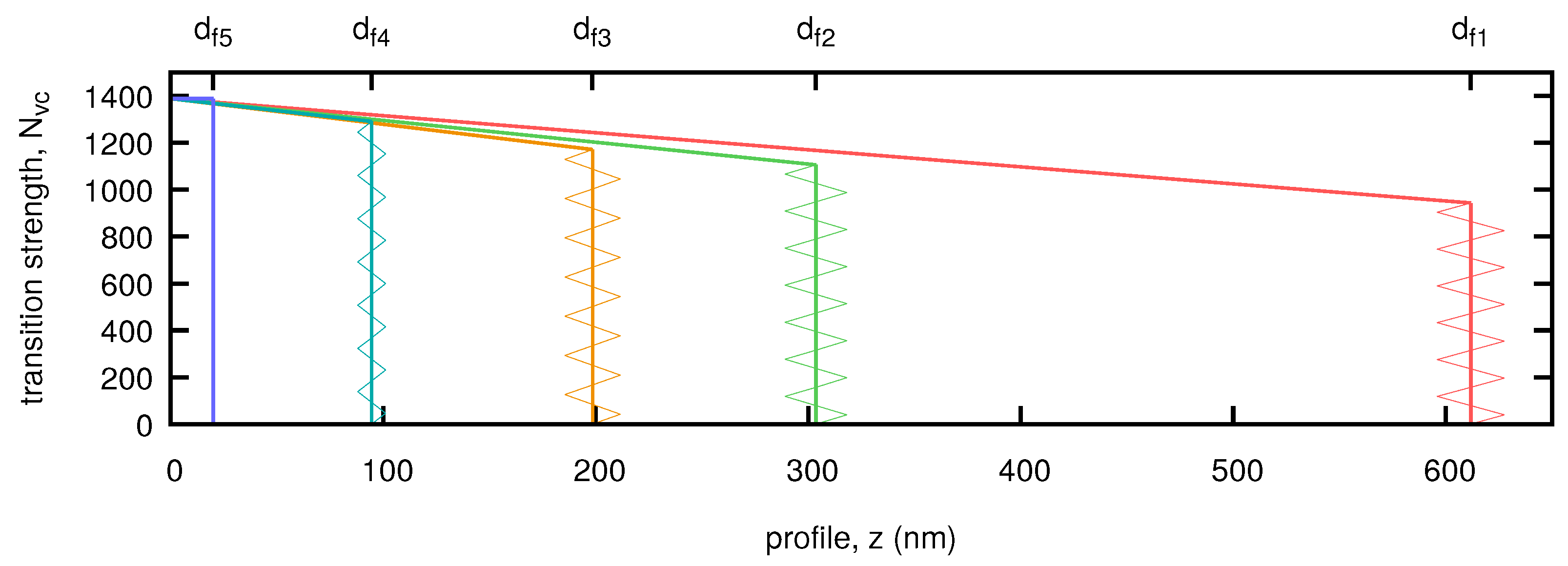
The density profile of the porous GdF3 film is in principle proportional to the transition strength profile of interband excitations N vc ( z ) . Figure 2 shows the transition strength profiles of all five samples calculated on the basis of the values listed in Table 1 and Table 2. The rough surfaces are indicated by zigzag lines with a range corresponding to 3 σ in this figure. It is evident that for a given value of z, the transition strength (density) of the thicker films is larger than for the thinner films. This can be explained by assuming that the material is not deposited only on the tops of the films but also partially into the pores during the growth of these films. The estimates of the packing densities on the tops of the films with respect to the bottoms of the films calculated as the ratio N vc , t / N vc , b are shown in Table 2. These estimates show a decrease with film thickness. This is not surprising because the size of crystals in this polycrystalline film grows with thickness, which results in larger pores.
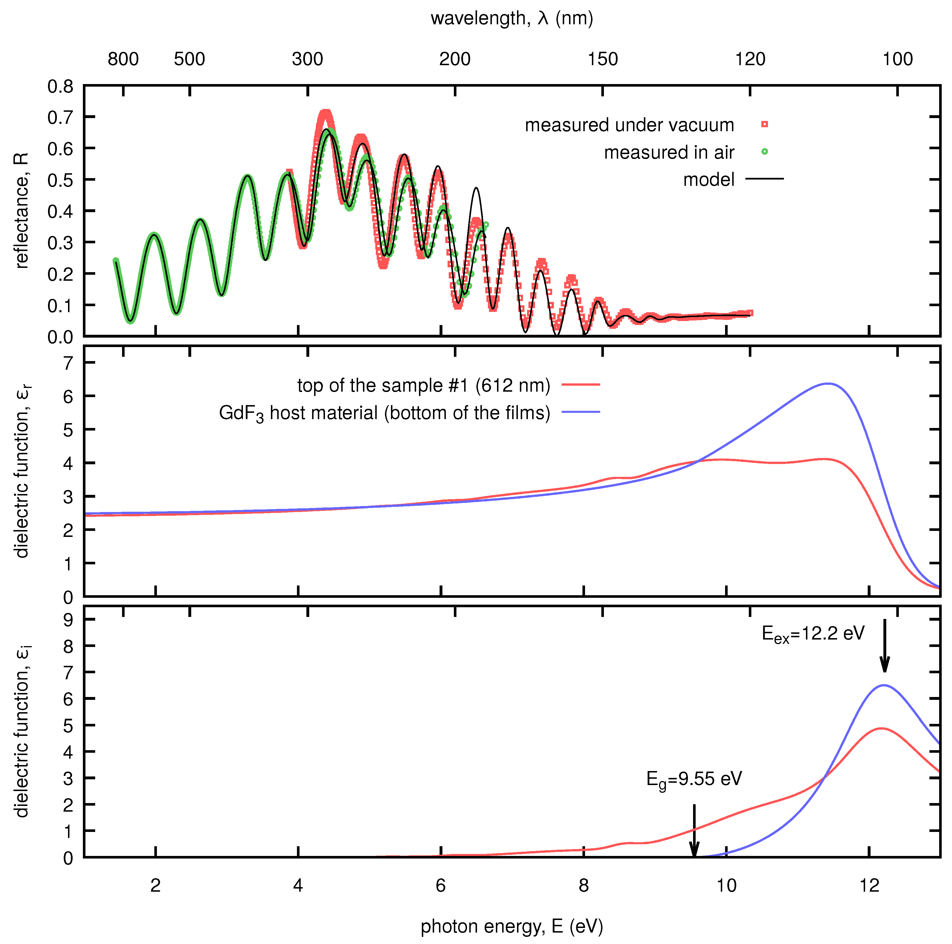
The spectral dependencies of the dielectric function on the top and bottom of the thickest inhomogeneous GdF3 film are shown in Figure 3. The excitonic structure centered around 12.2 eV, which is described by the parameters listed in Table 2, lies beyond the spectral range of the experimental data. Moreover, only reflectance data measured by the VUV spectrophotometer were available above 6.5 eV. Therefore, the credibility of the optical constants in this spectral region, and especially above 10 eV where the spectral range of the VUV spectrophotometer ends, is limited.
The reflectance spectra measured at near normal incidence using the VUV spectrophotometer under vacuum and using the standard instrument in air are also shown in 
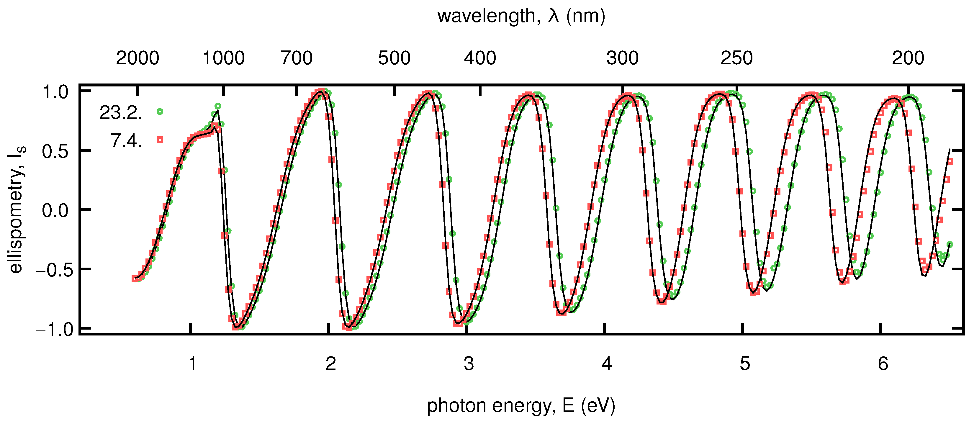
Figure 3. Evidently, these data do not coincide very well, which is caused by the volatility of the components adsorbed in the pores. The adsorbed components are strongly influenced by the surrounding conditions. Even the optical measurements performed under the same experimental conditions on the same sample can differ in a significant way, because these components are not stable in time. This is evident from the two ellipsometric measurements taken on the same sample six weeks apart, which are shown in Figure 4. The amount of adsorbed material is almost impossible to control; thus, the concentration of the volatile components was modeled separately for each experimental data point. Only one parameter, the transition strength of excitations involving the localized states N loc , was used for this purpose. As mentioned in the part devoted to the dispersion models, this parameter exhibits a linear profile, with zero at the bottom of the films. This means that while the dielectric function on the bottoms of the films is the same for all the samples, the dielectric function on the tops of the films is different not only for different samples, but it is slightly different also for different measurements (the one in Figure 3 corresponds to the thickest film and measurement by the VUV spectrophotometer). The values of N loc are listed in Table 3; the other dispersion parameters describing localized states, which are common to all samples and measurements, are listed in Table 4. From the dates of measurements shown in Table 3, it is evident that the amount of adsorbed material increased with passing time.
Strictly speaking, the Urbach energy should be used for a weak absorption below the band gap energy of solid materials (such as crystalline or amorphous semiconductors, glasses, etc.). The Urbach energy is in the order of tens of meV. In this work, the Urbach energy is also used more loosely for absorption on adsorbed components. From this point of view, the much higher value of the Urbach energy should not be surprising.

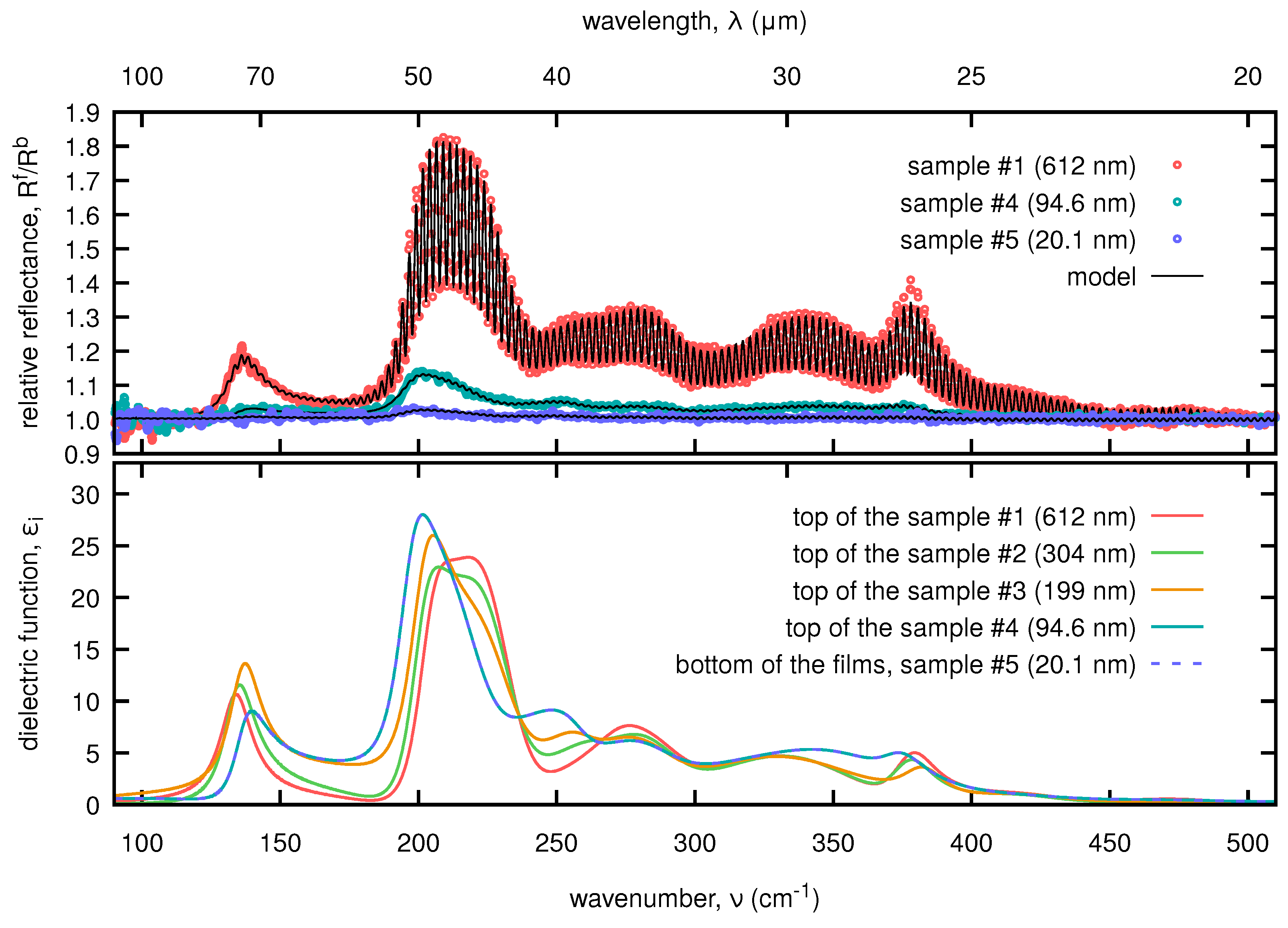
7.3. Phonon Excitations

The phonon absorption spectra of GdF3 are located in the far-infrared region as can be seen in Figure 5, where the high-resolution relative reflectance spectra of three selected samples are plotted. The spectral resolution of the FIR spectrophotometry data is 1 cm−1; thus, the interference patterns originating in the substrate were measured. Therefore, the influence of the substrate must be taken into account by a partially coherent model. Note that the interference observed in the substrate allowed us to determine its thickness with high precision (see Table 1). The evident evolution of the response function with sample thickness can be seen in the bottom part of the Figure 5, which shows the imaginary parts of the dielectric functions in the FIR region. The shape of the phonon structure is influenced by the structural changes in the GdF3 host material. It should be noted that in the spectral region below 250 cm 1 , only the spectrophotometric experimental data were measured, which influences the accuracy of the determined dielectric function in this region. From the relative reflectance data for the thinnest GdF3 film (sample #5), it can be seen that the one-phonon structures are at the level of the measurement noise. Therefore, it was assumed that the the phonon response function at the bottom of this film is the same as on the top of sample #4. That is why the response functions of the two thinnest films in Figure 5 overlap. The dispersion parameters of the phonon contributions of the GdF3 host material are listed in Table 5 and Table 6. The last lines of these tables show the total transition strengths of the crystalline and disordered phases and their sum. One can see the increase in the crystalline phase and the decrease in the disordered phase with increasing thickness of the films. The total transition strengths of both phases decrease with film thickness. This corresponds to the decrease in the packing density calculated as the ratio of the total transition strengths of phonon excitations of the given sample and that corresponding to sample 5, which is assumed to be completely dense (see Table 6). The reason for the discrepancy between the packing densities calculated from the transition strengths of electronic excitations and phonon excitations could be that it was not possible to correctly determine the transition strength of the thinnest sample (as explained above), which is used as a reference with 100% packing density.
It should be noted that there are also two weak absorption peaks at wavenumbers 418 cm−1 and 473 cm−1 representing multi-phonon excitations.
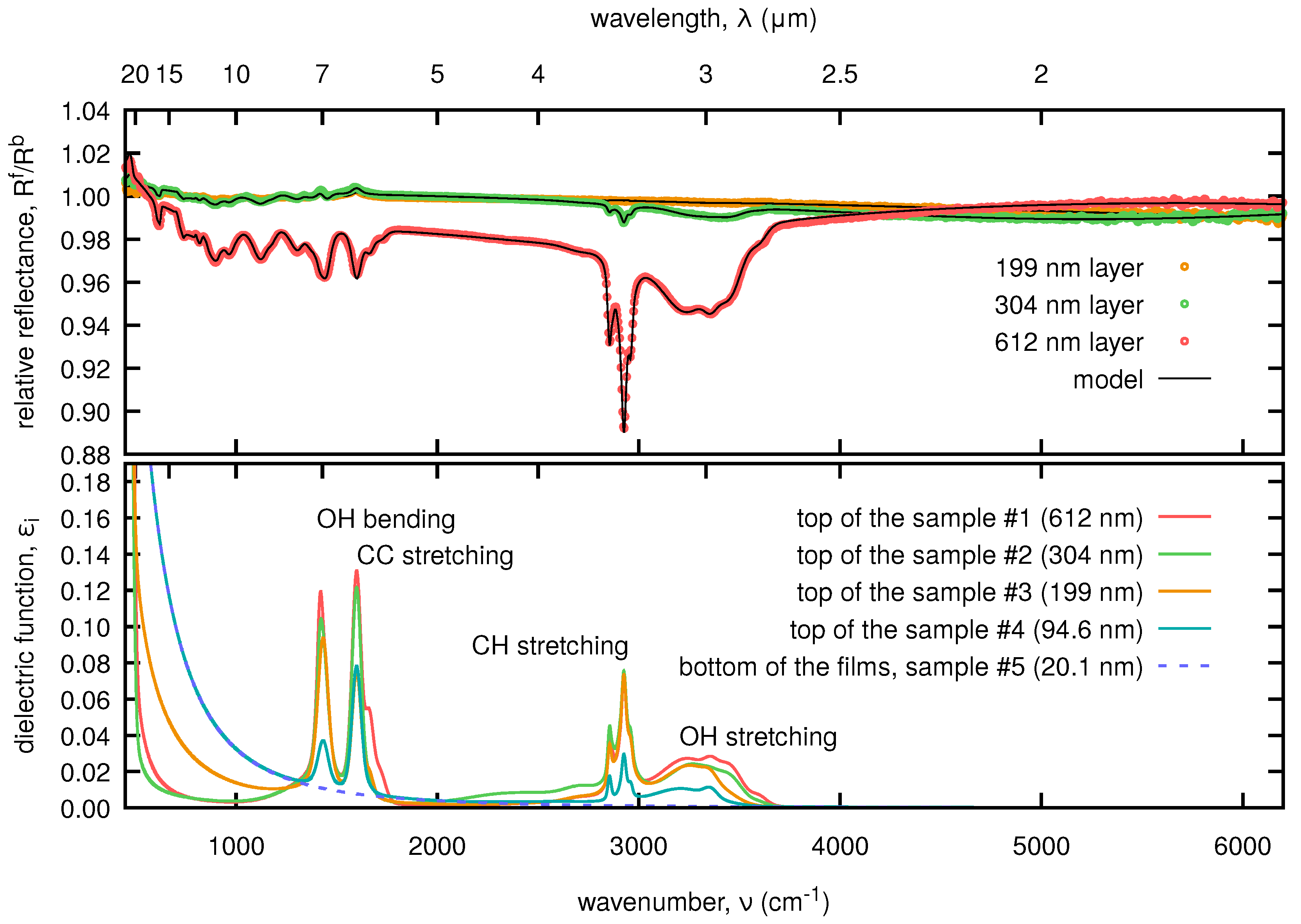
In the mid-infrared region one can see the vibration spectra of adsorbed components. The spectral resolution 8 cm−1 of the MIR spectrophotometry is much lower than that of the FIR spectrophotometry, and the interference patterns in the substrate are not observed in this case. The top panel of Figure 6 shows the relative reflectance spectra for the three thickest films. The characteristic fingerprints of OH (water) and CH (organics) vibrations in the region from 2800 to 3600 cm−1 are clearly visible in these spectra. Thus, it is apparent that the adsorbed components consist of water and organic molecules. In the region below 1800 cm−1, not only the vibration spectra of the adsorbed components, but also the multi-phonon absorption in the silicon substrate can be seen. In the bottom panel of Figure 6, the imaginary parts of the dielectric functions of the GdF3 films are plotted. It is easy to identify the characteristic absorption peaks of water and organic components even in the region where they overlap with the multi-phonon absorption spectra of silicon. Since the focus of this work is on the optical characterization of GdF3 host material and not on the exact characterization of the adsorbed components, only rough identification of the vibration spectra in the MIR region was performed.
The absorption structures of adsorbed components were modeled using 19 symmetric Voigt peaks with different transition strengths used for individual data sets. The strengths of the absorption structures were fitted independently for each measurement covering the MIR spectral region. In all other cases, these strengths were fixed in values determined for the MIR transmittance measurement. The other parameters of these peaks, i.e., the position, width and shape parameters, are common for all the experimental data.

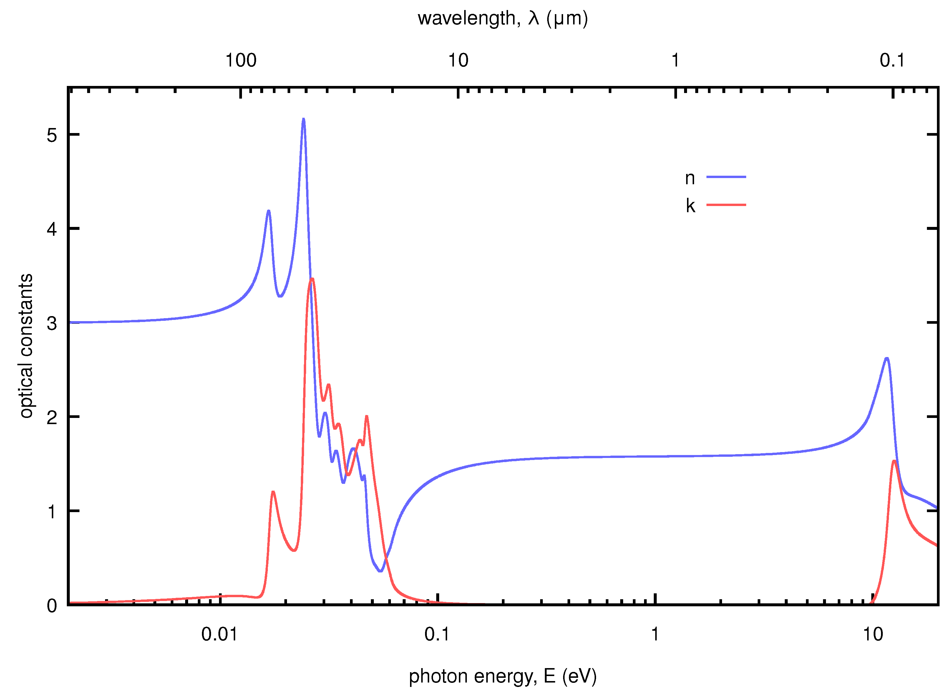
7.4. Optical Constants

The optical constants of the host GdF3 material, i.e., those corresponding to the bottoms of the films where they are assumed to be dense, are shown in Figure 7. The tabulated data can be found in the Supplementary Materials. The refractive index at 193 nm is 1.688, which is in good agreement with the values 1.68–1.69 published in [20].
The tabulated data for the optical constants of float-zone silicon substrates and the NOLs can be also found in the Supplementary Materials.

8. Conclusions

The optical characterization of gadolinium fluoride (GdF3) films was performed using the universal dispersion model [1] implemented in newAD2 software [22]. In the framework of this dispersion model, the asymmetric peak approximation with the Voigt broadening function was used to describe the one-phonon absorption. The ellipsometric and spectrophotometric experimental data measured for five samples in a wide spectral range using several instruments were processed simultaneously. The nominal thicknesses of the films ranged from 20 to 600 nm. The films exhibited several imperfections, which were found to be more severe for thicker films; namely, surface roughness and refractive index profile. It was shown that the optical properties of the thicker films change over time due to the volatile adsorbed components. The adsorbed components were identified as water and organics from the IR absorption spectra. All these defects suggest that the films have a porous structure. For the precise characterization of the GdF3 host material, it was necessary to include this instability of the optical properties together with the imperfection of these films in the model used in the optical characterization.
Although the films are far from ideal, the thinner films are not affected by these defects as much as the thicker ones; therefore, the optical properties obtained in this work can be used to describe these films in thin-film systems designed for the ultraviolet spectral region.
The presented method of optical characterization can be applied to a wide range of dielectric materials exhibiting porosity, surface roughness and refractive index profile, i.e., especially for other fluoride films used in multilayer coatings.

Supplementary Materials

The following supporting information can be downloaded at: https://www.mdpi.com/article/10.3390/coatings13020218/s1, Figure S1: Spectral dependencies of the generalized ellipsometric parameters displayed for the 612 nm thick film #1 (measured from the front side); Figure S2: Spectral dependencies of the generalized ellipsometric parameters displayed for the 304 nm thick film #2 (measured from the front side); Figure S3: Spectral dependencies of the generalized ellipsometric parameters displayed for the 199 nm thick film #3 (measured from the front side); Figure S4: Spectral dependencies of the generalized ellipsometric parameters displayed for the 94.6 nm thick film #4 (measured from the front side); Figure S5: Spectral dependencies of the generalized ellipsometric parameters displayed for the 20.1 nm thick film #5 (measured from the front side); Figure S6: Spectral dependencies of the generalized ellipsometric parameters displayed for the 612 nm thick film #1 (measured from the back side); Figure S7: Spectral dependencies of the generalized ellipsometric parameters displayed for the 304 nm thick film #2 (measured from the back side); Figure S8: Spectral dependencies of the generalized ellipsometric parameters displayed for the 199 nm thick film #3 (measured from the back side); Figure S9: Spectral dependencies of the generalized ellipsometric parameters displayed for the 94.6 nm thick film #4 (measured from the back side); Figure S10: Spectral dependencies of the generalized ellipsometric parameters displayed for the 20.1 nm thick film #5 (measured from the back side); Figure S11: Spectral dependencies of the difference ellipsometric quantities displayed for the 612 nm thick film #1; Figure S12: Spectral dependencies of the difference ellipsometric quantities displayed for the 304 nm thick film #2; Figure S13: Spectral dependencies of the difference ellipsometric quantities displayed for the 199 nm thick film #3; Figure S14: Spectral dependencies of the difference ellipsometric quantities displayed for the 94.6 nm thick film #4; Figure S15: Spectral dependencies of the difference ellipsometric quantities displayed for the 20.1 nm thick film #5; Figure S16: Spectral dependencies of the spectrophotometric quantities displayed for the 612 nm thick film; Figure S17: Spectral dependencies of the spectrophotometric quantities displayed for the 304 nm thick film; Figure S18: Spectral dependencies of the spectrophotometric quantities displayed for the 199 nm thick film; Figure S19: Spectral dependencies of the spectrophotometric quantities displayed for the 94.6 nm thick film; Figure S20: Spectral dependencies of the spectrophotometric quantities displayed for the 20.1 nm thick film; Figure S21: Spectral dependencies of the spectrophotometric quantities displayed for the 612 nm thick film; Figure S22: Spectral dependencies of the spectrophotometric quantities displayed for the 304 nm thick film; Figure S23: Spectral dependencies of the spectrophotometric quantities displayed for the 199 nm thick film; Figure S24: Spectral dependencies of the spectrophotometric quantities displayed for the 94.6 nm thick film; Figure S25: Spectral dependencies of the spectrophotometric quantities displayed for the 20.1 nm thick film; Figure S26: Spectral dependencies of the generalized ellipsometric parameters displayed for the 612 nm thick film (first measurement); Figure S27: Spectral dependencies of the generalized ellipsometric parameters displayed for the 612 nm thick film (second measurement); Figure S28: Spectral dependencies of the generalized ellipsometric parameters displayed for the 304 nm thick film; Figure S29: Spectral dependencies of the generalized ellipsometric parameters displayed for the 199 nm thick film; Figure S30: Spectral dependencies of the generalized ellipsometric parameters displayed for the 94.6 nm thick film; Figure S31: Spectral dependencies of the generalized ellipsometric parameters displayed for the 20.1 nm thick film; Figure S32: Spectral dependencies of the back side ellipsometry of all the samples; Figure S33: Spectral dependencies of the relative reflectance of all the films; Figure S34: Spectral dependencies of the reflectance of all the films; Figure S35: AFM topography of 612 nm thick GdF3 film (sample #1); Figure S36: AFM topography of 304 nm thick GdF3 film (sample #2); Figure S37: AFM topography of 199 nm thick GdF3 film (sample #3); Figure S38: AFM topography of 94.6 nm thick GdF3 film (sample #4); Figure S39: AFM topography of 20.1 nm thick GdF3 film (sample #5); Figure S40: Penalization functions for κ = 10; Figure S41: Spectral dependence of the FIR and MIR relative reflectances (the ratio of front and back reflectance) in multi-phonon region displayed for chosen GdF3 film (top panel) and spectral dependencies of the imaginary part of dielectric functions on the top the film (bottom panel); Figure S42: The plot of GdF3 optical constants; Figure S43: The plot of float zone silicon optical constants; Figure S44: The plot of silicon NOL optical constants; Table S1: List of data sets used for optical chareacterization; Table S2: Dispersion parameters of multi-phonon contributions.

Author Contributions

Conceptualization, D.F.; methodology, D.F. and J.V.; software, D.F., J.V. and P.F.; formal analysis, D.F. and P.K.; investigation, D.F., J.V. and J.D.; resources, D.Š. and J.B.; data curation, D.F., J.V., P.F., P.K., J.B. and D.Š.; writing—original draft preparation, D.F., J.D. and J.V.; writing—review and editing, D.F., J.D. and J.V.; visualization, D.F.; supervision, I.O.; funding acquisition, I.O. All authors have read and agreed to the published version of the manuscript.

Funding

This work was supported by the project FV40328 funded by the Ministry of Industry and Trade of the Czechia and by the projects LM2018097 and LM2018110 funded by the Ministry of Education, Youth and Sports of the Czech Republic.

Institutional Review Board Statement

Not applicable.

Informed Consent Statement

Not applicable.

Data Availability Statement

Data presented in this study that are not in the Supplementary Materials are available on request from the corresponding author.

Acknowledgments

The optical measurements were performed on the CEPLANT and CEITEC Nano Research Infrastructure.

Conflicts of Interest

The authors declare no conflict of interest. The funders had no role in the design of the study; in the collection, analyses, or interpretation of data; in the writing of the manuscript; or in the decision to publish the results.

Abbreviations

The following abbreviations are used in this manuscript:
UDMuniversal dispersion model
APSadvanced plasma source
QCMquartz crystal microbalance
LMALevenberg–Marquardt algorithm
NOLnative oxide layer
RMSroot-mean-square
RRTRayleigh–Rice theory
FWHMfull-width at half-maximum
AFMatomic force microscopy
UVultraviolet
VISvisible
IRinfrared
VUVvacuum ultraviolet
DUVdeep ultraviolet
UVVultraviolet and visible
MIRmid-infrared
FIRfar-infrared

References

  1. Franta, D.; Vohánka, J.; Čermák, M. Universal Dispersion Model for Characterization of Thin Films Over Wide Spectral Range. In Optical Characterization of Thin Solid Films; Springer Series in Surface Sciences; Stenzel, O., Ohlídal, M., Eds.; Springer: Cham, Switzerland, 2018; Volume 64, pp. 31–82. [Google Scholar]
  2. Franta, D.; Nečas, D.; Ohlídal, I. Universal dispersion model for characterization of optical thin films over wide spectral range: Application to hafnia. Appl. Opt. 2015, 54, 9108–9119. [Google Scholar] [CrossRef] [PubMed]
  3. Franta, D.; Nečas, D.; Ohlídal, I.; Giglia, A. Dispersion model for optical thin films applicable in wide spectral range. In Optical Systems Design 2015: Optical Fabrication, Testing, and Metrology V; SPIE: Bellingham, WA, USA, 2015; Volume 9628, p. 96281U. [Google Scholar]
  4. Franta, D.; Nečas, D.; Ohlídal, I.; Giglia, A. Optical characterization of SiO2 thin films using universal dispersion model over wide spectral range. In Photonics Europe 2016: Optical Micro- and Nanometrology VI; SPIE: Bellingham, WA, USA, 2016; Volume 9890, p. 989014. [Google Scholar]
  5. Franta, D.; Nečas, D.; Giglia, A.; Franta, P.; Ohlídal, I. Universal dispersion model for characterization of optical thin films over wide spectral range: Application to magnesium fluoride. Appl. Surf. Sci. 2017, 421, 424–429. [Google Scholar] [CrossRef]
  6. Franta, D.; Vohánka, J.; Bránecký, M.; Franta, P.; Čermák, M.; Ohlídal, I.; Čech, V. Optical properties of the crystalline silicon wafers described using the universal dispersion model. J. Vac. Sci. Technol. B 2019, 37, 062907. [Google Scholar] [CrossRef]
  7. Franta, D.; Mureșan, M.G. Wide spectral range optical characterization of yttrium aluminum garnet (YAG) single crystal by universal dispersion model. Opt. Mater. Express 2021, 11, 3930–3945. [Google Scholar] [CrossRef]
  8. Yoshida, T.; Nishimoto, K.; Sekine, K.; Etoh, K. Fluoride antireflection coatings for deep ultraviolet optics deposited by ion-beam sputtering. Appl. Opt. 2006, 45, 1375–1379. [Google Scholar] [CrossRef] [PubMed]
  9. Pei, L.; Jiaqi, Z.; Yuankun, Z.; Jiecai, H. Preparation and optical properties of sputtered-deposition yttrium fluoride film. Nucl. Instrum. Methods Phys. Res. B 2013, 307, 429–433. [Google Scholar] [CrossRef]
  10. Liu, M.C.; Lee, C.C.; Kaneko, M.; Nakahira, K.; Takano, Y. Microstructure-and composition-related characteristics of LaF3 thin films at 193 nm. Opt. Eng. 2006, 45, 083801. [Google Scholar] [CrossRef]
  11. Liu, M.C.; Lee, C.C.; Kaneko, M.; Nakahira, K.; Takano, Y. Microstructure-related properties at 193 nm of MgF2 and GdF3 films deposited by a resistive-heating boat. Appl. Opt. 2006, 45, 1368–1374. [Google Scholar] [CrossRef]
  12. Kaiser, U.; Kaiser, N.; Weiβbrodt, P.; Mademann, U.; Hacker, E.; Müller, H. Structure of thin fluoride films deposited on amorphous substrates. Thin Solid Film. 1992, 217, 7–16. [Google Scholar] [CrossRef]
  13. Yazicigil, O.G.; Rafik, D.; Vorontsov, V.; King, A.H. Structural control of lithium fluoride thin films. MRS Online Proc. Libr. 2005, 875, O12.9. [Google Scholar] [CrossRef]
  14. Shakoury, R.; Matos, R.S.; da Fonseca Filho, H.D.; Rezaee, S.; Arman, A.; Boochani, A.; Jurečka, S.; Zelati, A.; Mardani, M.; Ţălu, Ş. Investigation of deposition temperature effect on spatial patterns of MgF2 thin films. Microsc. Res. Tech. 2022. [Google Scholar] [CrossRef] [PubMed]
  15. Chindaudom, P.; Vedam, K. Characterization of inhomogeneous transparent thin films on transparent substrates by spectroscopic ellipsometry: Refractive indices n(λ) of some fluoride coating materials. Appl. Opt. 1994, 33, 2664–2671. [Google Scholar] [CrossRef] [PubMed]
  16. Atosuo, E.; Mizohata, K.; Mattinen, M.; Mäntymäki, M.; Vehkamäki, M.; Leskelä, M.; Ritala, M. Atomic layer deposition of GdF3 thin films. J. Vac. Sci. Technol. A 2022, 40, 022402. [Google Scholar] [CrossRef]
  17. Jin, J.; Jin, C.; Li, C.; Deng, W.; Yao, S. Influence of substrate temperatures on the properties of GdF3 thin films with quarter-wave thickness in the ultraviolet region. Appl. Opt. 2015, 54, 5117–5122. [Google Scholar] [CrossRef] [PubMed]
  18. Wang, J.; Maier, R.; Dewa, P.G.; Schreiber, H.; Bellman, R.A.; Elli, D.D. Nanoporous structure of a GdF3 thin film evaluated by variable angle spectroscopic ellipsometry. Appl. Opt. 2007, 46, 3221–3226. [Google Scholar] [CrossRef]
  19. Dumas, L.; Quesnel, E.; Robic, J.Y.; Pauleau, Y. Characterization of magnesium fluoride thin films deposited by direct electron beam evaporation. J. Vac. Sci. Technol. A 2000, 18, 465–469. [Google Scholar] [CrossRef]
  20. Thielsch, R.; Heber, J.; Uhlig, H.; Kaiser, N. Optical, structural, and mechanical properties of gadolinium tri-fluoride thin films grown on amorphous substrates. In Advances in Optical Thin Films II; SPIE: Bellingham, WA, USA, 2005; Volume 5963, p. 59630O. [Google Scholar]
  21. Ohlídal, I.; Vohánka, J.; Čermák, M.; Franta, D. Ellipsometry of Layered Systems. In Optical Characterization of Thin Solid Films; Springer Series in Surface Sciences; Stenzel, O., Ohlídal, M., Eds.; Springer: Cham, Switzerland, 2018; Volume 64, pp. 233–267. [Google Scholar]
  22. Franta, D.; Nečas, D.; Vohánka, J. Software for Optical Characterization newAD2. Available online: http://newad.physics.muni.cz (accessed on 12 January 2023).
  23. PVM (Parallel Virtual Machine). Available online: http://www.csm.ornl.gov/pvm/ (accessed on 12 January 2023).
  24. Marquardt, W.D. An algorithm for least squares estimation of nonlinear parameters. J. Soc. Ind. Appl. Math. 1963, 11, 431–441. [Google Scholar] [CrossRef]
  25. More, J.J. The Levenberg–Marquardt algorithm: Implementation and theory. In Lecture Notes in Mathematics; Watson, G.A., Ed.; Springer–Verlag: Berlin, Germany, 1978; Volume 630, pp. 106–116. [Google Scholar]
  26. Franta, D.; Dubroka, A.; Wang, C.; Giglia, A.; Vohánka, J.; Franta, P.; Ohlídal, I. Temperature-dependent dispersion model of float zone crystalline silicon. Appl. Surf. Sci. 2017, 421, 405–419. [Google Scholar] [CrossRef]
  27. Vohánka, J.; Ohlídal, I.; Ženíšek, J.; Vašina, P.; Čermák, M.; Franta, D. Use of the Richardson extrapolation in optics of inhomogeneous layers: Application to optical characterization. Surf. Interface Anal. 2018, 50, 757–765. [Google Scholar] [CrossRef]
  28. Franta, D.; Ohlídal, I. Ellipsometric Parameters and Reflectances of Thin Films with Slightly Rough Boundaries. J. Mod. Opt. 1998, 45, 903–934. [Google Scholar] [CrossRef]
  29. Vohánka, J.; Čermák, M.; Franta, D.; Ohlídal, I. Efficient method to calculate the optical quantities of multi-layer systems with randomly rough boundaries using the Rayleigh–Rice theory. Phys. Scr. 2019, 94, 045502. [Google Scholar] [CrossRef]
  30. Campi, D.; Coriasso, C. Prediction of optical properties of amorphous tetrahedrally bounded materials. J. Appl. Phys. 1988, 64, 4128–4134. [Google Scholar] [CrossRef]
  31. Campi, D.; Coriasso, C. Relationships between optical properties and band parameters in amorphous tetrahedrally bonded materials. Mater. Lett. 1988, 7, 134–137. [Google Scholar] [CrossRef]
  32. Franta, D.; Čermák, M.; Vohánka, J.; Ohlídal, I. Dispersion models describing interband electronic transitions combining Tauc’s law and Lorentz model. Thin Solid Film. 2017, 631, 12–22. [Google Scholar] [CrossRef]
  33. Thomas, M.E.; Andersson, S.K.; Sova, R.M.; Joseph, R.I. Frequency and temperature dependence of the refractive index of sapphire. Infrared Phys. Technol. 1998, 39, 235–249. [Google Scholar] [CrossRef]
  34. De Sousa Meneses, D.; Brun, J.F.; Rousseau, B.; Echegut, P. Polar lattice dynamics of the MgAl2O4 spinel up to the liquid state. J. Phys. Condens. Matter 2006, 18, 5669–5686. [Google Scholar] [CrossRef]
  35. De Sousa Meneses, D.; Malki, M.; Echegut, P. Structure and lattice dynamics of binary lead silicate glesses investigated by infrared spectroscopy. J. Non-Cryst. Solids 2006, 352, 769–776. [Google Scholar] [CrossRef]
  36. Kitamura, R.; Pilon, L.; Jonasz, M. Optical constants of silica glass from extreme ultraviolet to far infrared at near room temperature. Appl. Opt. 2007, 46, 8118–8133. [Google Scholar] [CrossRef]
  37. Abramowitz, M.; Stegun, I.A. (Eds.) Handbook of Mathematical Functions with Formulas, Graphs, and Mathematical Tables; Applied Mathematics Series—55; National Bureau of Standards: Washington, DC, USA, 1964. [Google Scholar]
  38. Tauc, J. Optical Properties of Non-Crystaline Solids. In Optical Properties of Solids; Abelès, F., Ed.; North–Holland: Amsterdam, The Netherlands, 1972; pp. 277–313. [Google Scholar]
  39. Humlíček, J. Optimized computation of the Voigt and complex probability function. J. Quant. Spectrosc. Radiat. Transf. 1982, 27, 437–444. [Google Scholar] [CrossRef]
  40. Brendel, R.; Bormann, D. An infrared dielectric function model for amorphous solids. J. Appl. Phys. 1992, 71, 1–6. [Google Scholar] [CrossRef]
  41. De Sousa Meneses, D.; Gruener, G.; Malki, M.; Echegut, P. Causal Voigt profile for modeling reflectivity spectra of glasses. J. Non-Cryst. Solids 2005, 351, 124–129. [Google Scholar] [CrossRef]
  42. Abrarov, S.M.; Quine, B.M. Efficient algorithmic implementation of the Voigt/complex error function based on exponential series approximation. Appl. Math. Comput. 2011, 218, 1894–1902. [Google Scholar] [CrossRef]
  43. Kischkat, J.; Peters, S.; Gruska, B.; Semtsiv, M.; Chashnikova, M.; Klinkmüller, M.; Fedosenko, O.; Machulik, S.; Aleksandrova, A.; Monastyrskyi, G.; et al. Mid-infrared optical properties of thin films of aluminum oxide, titanium dioxide, silicon dioxide, aluminum nitride, and silicon nitride. Appl. Opt. 2012, 71, 6789–6798. [Google Scholar] [CrossRef] [PubMed]
  44. Nečas, D.; Klapetek, P. Gwyddion: An open-source software for SPM data analysis. Cent. Eur. J. Phys. 2012, 10, 181–188. [Google Scholar] [CrossRef]
Figure 1. Schematic diagram of the structural model. The dashed lines represent the mean planes of the boundaries.
Coatings 13 00218 g001
Figure 2. Transition strength profiles of the GdF3 films. The zigzag lines indicate the surface roughness. Their amplitude corresponds to the value of 3 σ .
Coatings 13 00218 g002
Figure 3. Spectral dependencies of near-normal reflectances R measured by the UV-visible and VUV spectrophotometers for the thickest 612 nm GdF3 film (upper panel) using two spectrophotometers. The bottom two panels show the dielectric functions at the top and bottom of this film.
Coatings 13 00218 g003
Figure 4. Spectral dependencies of the associated ellipsometric quantity I s measured for the thickest 612 nm GdF3 film at 65 (sample #1) shortly after the film deposition and six weeks later, during which it was exposed to air. The dates of the measurements are stated in the legend.
Coatings 13 00218 g004
Figure 5. Spectral dependencies of the relative reflectances in the FIR region (the ratio of the front and back reflectances) displayed for three selected GdF3 films (top panel) and spectral dependencies of the imaginary parts of the dielectric functions on the tops and bottoms of all the films (bottom panel).
Coatings 13 00218 g005
Figure 6. Spectral dependencies of the relative reflectances in the MIR region (the ratio of the front and back reflectances) displayed for three selected GdF3 films (top panel) and the spectral dependencies of the imaginary parts of the dielectric functions on the tops and bottoms of all the films (bottom panel).
Coatings 13 00218 g006
Figure 7. Optical constants of the host GdF3 material.
Coatings 13 00218 g007
Table 1. Structural parameters of GdF3 films determined in the optical characterization and by AFM. All listed values are in nanometers with the exception of the substrate thickness, which is in micrometers. The uncertainty of the fited parameters is shown using concise bracket notation.
Sample#1#2#3#4#5
Optical characterization
Nominal thickness60030020010020
Film thickness d f 611.75(6)303.62(2)198.53(2)94.58(2)20.075(15)
RMS of roughness σ 10.55(3)9.72(2)8.70(2)4.38(3)0
Autocorr. length τ 22.79(7)
Transition layer d t 0.252(15)
Substrate thickness d s 577.607(2)577.897(2)577.809(2)577.727(2)577.514(2)
Backside layer d o 2.049(4)2.033(4)2.620(3)2.632(4)3.308(5)
AFM
RMS of roughness8.558.877.254.570.72
Autocorr. length3624222016
Table 2. Selected dispersion parameters describing the electronic structure of GdF3 host material forming porous inhomogeneous films. Note that sample #5 is assumed to be homogeneous dense film with transition strength N vc , b . The last line shows the estimates of the packing densities of the tops of the films with respect to the bottoms of the films. The uncertainty of the fited parameters is shown using concise bracket notation.
Sample#1#2#3#4#5
Band gap energy E g (eV)9.550(8)
Exciton energy E ex (eV)12.218(11)
Broadening parameter B ex (eV)1.70(3)
Relative transition strength A ex 0.1515(15)
Transition str. (top) N vc , t ( eV 2 )942(3)1105(3)1170(3)1290(3)1387(3)
Transition str. (bottom) N vc , b ( eV 2 )1387(3)
Packing density N vc , t / N vc , b (%)67.979.784.393.0100.0
Table 3. Dispersion parameter N loc ( eV 2 ) describing the strength of electron excitations involving localized states of volatile adsorbed components in GdF3 porous inhomogeneous films. The value of the parameter differs for individual measurements, where the names of the individual measured data consist of the following acronyms: R—reflectance, T—transmittance, E—ellipsometry, VUV—vacuum ultraviolet, UVV—ultraviolet and visible, MIR—mid-infrared, FIR—far-infrared and IR—infrared. The superscripts show the dates of measurements. Note that two values corresponding to two different measurements are shown for E-UVV of sample 1. The uncertainty of the fited parameters is shown using concise bracket notation.
Sample#1#2#3#4#5
R-VUV196(4) 22.4 . 122(3) 22.4 . 101(2) 24.5 . 86(2) 26.5 . 0
R-UVV124(3) 15.4 . 81(2) 15.4 . 59.6(15) 15.4 . 34.1(14) 8.4 . 0
T-MIR & T-FIR121(3) 14.4 . 110(6) 15.4 . 125(3) 14.4 . 102(48) 14.4 . 0
R-MIR & R-FIR166(4) 15.4 . 121(3) 15.4 . 125.1 15.4 . 102.2 15.4 . 0
E-UVV39(2) 23.2 . 89(3) 7.4 . 79(2) 15.4 . 0.0(9) 22.2 . 19.3(12) 18.2 . 0
E-IR176(4) 22.4 . 81(2) 24.4 . 35(2) 29.4 . 76(4) 4.5 . 0
Table 4. Dispersion parameters describing excitations involving localized states of adsorbed components.
j = 1 j = 2 j = 3 j = 4 j = 5
Relative strength A loc , j ( 10 3 )179(10)3.7(2)11.1(5)0.53(2)0.092(4)
Mean energy E loc , j (eV)10.37(3)8.558(4)7.75(2)6.216(2)5.268(3)
Broadening parameter B loc , j (eV)0.89(2)0.183(5)0.667(11)0.154(2)0.121(3)
Band gap energy E g (eV)9.550(8)
Urbach energy E u (eV)2.16(4)
Table 5. Dispersion parameters corresponding to the one-phonon contributions from the crystalline phase. The uncertainty of the fited parameters is shown using concise bracket notation. Parameter M ph , 1 was calculated using condition (26). The last line shows the sum of all the transition strengths of the crystalline phase.
Sample#1#2#3#4 & #5
Transition strength N ph , 1 (10−3 eV2) 0.47 ( 2 ) 0.49 ( 3 ) 0.52 ( 3 ) 0.27 ( 2 )
Asymmetry M ph , 1 (10−3 eV2) 0.0504 0.1871 0.154 0.279
Resonant frequency ν ph , 1 (cm−1) 133.6 ( 5 ) 134.0 ( 5 ) 136.3 ( 7 ) 136.6 ( 5 )
Broadening β ph , 1 (cm−1) 14.1 ( 3 )
Lorentzian weight L ph , 1 1.00 ( 6 )
transition strength N ph , 2 (10−3 eV2) 1.02 ( 13 ) 0.99 ( 12 ) 1.32 ( 12 ) 1.34 ( 9 )
Asymmetry M ph , 2 (10−3 eV2) 1.4 ( 2 ) 1.45 ( 14 ) 1.3 ( 2 ) 1.24 ( 14 )
Resonant frequency ν ph , 1 (cm−1) 203.3 ( 5 ) 200.6 ( 4 ) 201.0 ( 5 ) 196.9 ( 3 )
Broadening β ph , 2 (cm−1) 18.4 ( 5 )
Lorentzian weight L ph , 2 0.98 ( 4 )
Transition strength N ph , 3 (10−3 eV2) 0.0 ( 4 ) 0.0 ( 2 ) 0.0 ( 3 ) 0.000 ( 13 )
Asymmetry M ph , 3 (10−3 eV2) 0.2 ( 3 ) 0.2 ( 2 ) 0.3 ( 2 ) 0.6 ( 3 )
resonant frequency ν ph , 1 (cm−1) 277 ( 7 ) 265 ( 3 ) 260 ( 4 ) 257.9 ( 7 )
Broadening β ph , 3 (cm−1) 23 ( 5 )
Lorentzian weight L ph , 3 1.0 ( 3 )
Transition strength N ph , 4 (10−3 eV2) 0.5 ( 3 ) 0.31 ( 14 ) 0.2 ( 3 ) 0.2 ( 2 )
Asymmetry M ph , 4 (10−3 eV2) 0.2 ( 3 ) 0.4 ( 3 ) 0.3 ( 2 ) 0.2 ( 2 )
Resonant frequency ν ph , 1 (cm−1) 282 ( 4 ) 285 ( 4 ) 285 ( 6 ) 284 ( 5 )
Broadening β ph , 4 (cm−1) 28 ( 3 )
Lorentzian weight L ph , 4 0.0 ( 7 )
Transition strength N ph , 5 (10−3 eV2) 2.0 ( 3 ) 1.7 ( 4 ) 1.4 ( 5 ) 1.6 ( 3 )
Asymmetry M ph , 5 (10−3 eV2) 1.2 ( 4 ) 1.5 ( 4 ) 0.9 ( 4 ) 1.3 ( 3 )
Resonant frequency ν ph , 1 (cm−1) 341 ( 4 ) 345 ( 4 ) 341 ( 6 ) 358 ( 4 )
Broadening β ph , 5 (cm−1) 67 ( 3 )
Lorentzian weight L ph , 5 0.6 ( 2 )
Transition strength N ph , 6 (10−3 eV2) 0.54 ( 10 ) 0.48 ( 10 ) 0.40 ( 7 ) 0.24 ( 4 )
Asymmetry M ph , 6 (10−3 eV2) 0.41 ( 7 ) 0.33 ( 7 ) 0.01 ( 7 ) 0.19 ( 6 )
Resonant frequency ν ph , 1 (cm−1) 376.8 ( 9 ) 376.1 ( 11 ) 382.5 ( 12 ) 372.8 ( 10 )
Broadening β ph , 6 (cm−1) 17.5 ( 7 )
Lorentzian weight L ph , 6 0.79 ( 12 )
Transition strength N ph , 7 (10−3 eV2) 0.77 ( 13 ) 0.53 ( 11 ) 0.0 ( 3 ) 0.18 ( 13 )
Asymmetry M ph , 7 (10−3 eV2) 0.8 ( 3 ) 0.7 ( 2 ) 0.57 ( 14 ) 0.50 ( 15 )
Resonant frequency ν ph , 1 (cm−1) 227.7 ( 13 ) 227.9 ( 13 ) 231 ( 3 ) 218 ( 2 )
Broadening β ph , 7 (cm−1) 21.4 ( 10 )
Lorentzian weight L ph , 7 0.0 ( 3 )
Crystalline phase j N ph , j (10−3 eV2) 5.351 4.468 3.818 3.752
Table 6. Dispersion parameters corresponding to the one-phonon contributions from the disordered phase. The uncertainty of the fited parameters is shown using concise bracket notation. The last three lines show the sum of the transition strengths of the disordered phase, the total transition strength calculated as a sum of the crystalline and disordered phases and the packing density calculated with respect to the top of sample #4.
Sample#1#2#3#4 & #5
Transition strength N ph , 8 (10−3 eV2) 0.7 ( 11 ) 1.7 ( 9 ) 3 ( 2 ) 5.3 ( 3 )
Resonant frequency ν ph , 8 (cm−1) 222 ( 7 )
Broadening β ph , 8 (cm−1) 203 ( 33 )
Lorentzian weight L ph , 8 1.0 ( 2 )
Transition strength N ph , 9 (10−3 eV2) 0.5 ( 12 ) 0.4 ( 9 ) 1 ( 3 ) 0.000 ( 5 )
Resonant frequency ν ph , 9 (cm−1) 199 ( 43 )
Broadening β ph , 9 (cm−1) 151 ( 60 )
Lorentzian weight L ph , 9 0 ( 2 )
Disordered phase j N ph , j (10−3 eV2) 1.274 2.11 3.855 5.279
Total transition str. j N ph , j (10−3 eV2) 6.625 6.578 7.673 9.032
Packing density (%) 73.4 72.8 85.0 100
Disclaimer/Publisher’s Note: The statements, opinions and data contained in all publications are solely those of the individual author(s) and contributor(s) and not of MDPI and/or the editor(s). MDPI and/or the editor(s) disclaim responsibility for any injury to people or property resulting from any ideas, methods, instructions or products referred to in the content.

