Review

A Review of Carbon-Based Conductive Inks and Their Printing Technologies for Integrated Circuits

1
Key Laboratory of Intelligent Manufacturing Technology, Shantou University, Ministry of Education, Shantou 515063, China
2
Foshan Bairui New Material Co., Ltd., Foshan 528000, China
*
Author to whom correspondence should be addressed.
Coatings 2023, 13(10), 1769; https://doi.org/10.3390/coatings13101769
Submission received: 14 September 2023 / Revised: 4 October 2023 / Accepted: 11 October 2023 / Published: 13 October 2023

Abstract

:
In recent years, researchers prepared composite conductive inks with high conductivity, high thermal conductivity, strong stability, and excellent comprehensive mechanical properties by combining carbon-based materials such as graphene and carbon nanotubes with metal-based materials. Through new electronic printing technologies, conductive inks can be used not only to promote the development of integrated circuits but also in various new electronic products. The conductive mechanism and the main types of conductive inks are introduced in this review. The advantages of electronic printing technology for preparing integrated circuits are analyzed. The research progress of fabricating integrated circuits with different electronic printing processes, such as screen printing, gravure printing, flexographic printing, and inkjet printing, are summarized. The development trend of carbon-based composite conductive ink for integrated circuits is prospected.

1. Introduction

With the world entering the information age, new technologies such as 5G, big data, the Internet of Things, artificial intelligence, and other new technologies are leading a new wave of industrial revolution. The electronic information industry has become a fundamental, leading, and strategic industry for the economic advancement of the nation. As the core field in the electronic information industry, the integrated circuit is crucial to the development of national defense security, aerospace, rail transportation, intelligent equipment, and other fields. The integrated circuit is a field in the high-tech industry that integrates various modern sciences such as microelectronics, physics and chemistry, optical components, semiconductor materials, precision machinery manufacturing, etc., with high technical barriers and enormous difficulties in research and development. In recent years, the continuous progress of advanced conductive inks and new electronic printing technologies have not only provided a new development path for the evolution of integrated circuits but also become a research hotspot in the field of integrated circuits. Conductive ink is a functional electronic material that is widely used in integrated circuits [1], flexible wearable electronics [2], 5G communication devices [3], radio frequency identification tags [4], solar cells [5], new energy vehicles [6], organic light-emitting displays, and other popular areas of electronic territory [7]. It also lies in the upstream link of the integrated circuit manufacturing industry chain, playing a crucial supporting role in the advancement and innovation of the integrated circuit manufacturing industry [8]. Due to newly developed conductive ink with excellent electrical properties, thermal properties, mechanical properties, and other kinds of excellent comprehensive performance, the essential application of conductive ink is to prepare integrated circuits through new electronic printing technologies.
Compared with the conventional processes of preparing integrated circuits (ICs) through prefabricated mask plates, thin film deposition, photolithography, etching, ion implantation, electroplating, and polishing, electronic printing technology can improve the production speed, simplify the preparation process, reduce processing costs, and eliminate the need for both a high processing temperature in a high-vacuum environment in the preparation process and the use of corrosive chemical reagents; it also offers tremendous advantages in the preparation of flexible integrated circuits and flexible electronic components [9]. With the constant development of electronic printing technology, the methods of preparing integrated circuits have also been further expanded and improved. The conductive mechanism of conductive ink for integrated circuit printing and the main types of conductive ink according to different requirements for integrated circuits are described in this review. The advantages and drawbacks of diverse types of conductive inks are compared. Moreover, the preparation and application of carbon-based and carbon-metal-based composite conductive inks are emphasized, and the benefits of new electronic printing technologies and their applications in the field of integrated circuits are discussed. Finally, based on the practical application requirements of integrated circuits, the development trend and research direction of conductive ink and electronic printing technology are analyzed.

2. Conductive Mechanism of Conductive Inks

Conductive ink is a functional electronic material consisting of a viscous ink mixture with a conductive function produced by uniformly dispersing the conductive functional phases in the carrier solvent, adding additives, and a certain amount of binder [10]. The prepared conductive ink is transferred to the substrate using different electronic printing methods [11]. After removing the nonconductive carrier solvent and the additive using low-temperature curing [12], high-temperature sintering [13], laser irradiation [14], and other postprocessing means, the volume of the conductive ink shrinks and the conductive functional phases are closely connected to form a conductive network, which can form a conductive pathway under the action of an external voltage to achieve conductive function [15]. The conductive mechanism of conductive inks is quite complex, and the microscopic and macroscopic levels are usually applied with different conductive mechanisms. So far, there are three main conductive mechanisms that are widely acknowledged by the academic community: the conductive channel mechanism, the tunneling effect theory, and the field emission effect.

2.1. Conductive Channel Mechanism

The conductive channel mechanism refers to the conductive channels in the conductive ink, which are formed by the direct contact of numerous conductive particles, resulting in the conductive behavior [16]. Before sintering, conductive particles in the organic carrier of the conductive ink are isolated from each other without the capacity to conduct electricity; during the sintering process of the conductive ink, the nonconductive organic carrier decomposes and volatilizes as the temperature increases, and the adhesive phase melts and contracts after absorbing heat, wetting the conductive functional phase and pulling the conductive functional phase to orderly rearrange through surface tension to achieve the conductive function, as displayed in Figure 1. The conductive channel mechanism, also known as percolation theory, is applicable to the macroscopic explanation of the system with a large percentage of conductive particles added [17]. Via continuously increasing the proportion of conductive particles added to the conductive ink up to a certain amount, the conductive particles that originally dispersed individually in the conductive ink contact each other to form tightly connected chainlike channels that can conduct electricity in all directions, thus substantially enhancing the conductive properties of the conductive ink [18]. There is a special value that indicates the percolation threshold for the addition of conductive particles. The percolation threshold depends on the type of conductive particles, organic carrier, bonding phase, and dispersion state in the conductive ink. The percolation threshold represents the minimum value for which high electrical conductivity via the conduction mechanism occurs. After the percolation threshold, the conductivity would continue to increase by one or more orders of magnitude as a function of filler loading. The printability and as-printed mechanical properties suffer if the loading gets too high. The optimal loading level may be different for diverse materials, applications, and printing techniques. The concentration of conductive particles in metal-based conductive inks often lies between 30% and 80%, and the high-temperature-resistant organic or inorganic chemicals are often chosen to be adhesives [19]. The concentration between 30% and 40% is suitable for inkjet printing. The concentration between 50% and 80% is usually used in screen printing due to the high viscosity. The conductive particle contents of polymer-based conductive ink are between 5% and 30% [20,21]. Polymer-based conductive ink is commonly used to print circuits using inkjet printing technology due to its low concentration. Due to the hydrophobic and agglomerative character of the carbon-based materials, the solids content of the carbon-based materials is usually varied in the range of 2% to 10% [22,23,24]. The concentration of graphene in carbon-based materials for screen printing can be as high as 10%, while its concentration for other printing methods is limited in the range of 2%–6%. To strengthen the conductivity, the solid content of conductive particles was improved from 10% to 30% through the formation of carbon-based composite ink with other excellent conductive metals or polymers [25,26,27]. A solids content of carbon-based composites of 30% is usually applied in screen printing, and a solids content of around 10% is suitable for other printing technologies.

2.2. Tunnel Effect Theory

The conductive channel mechanism explains the conductive phenomenon at the macroscopic level but cannot explain the following phenomena: even if massive conductive particles are exceedingly close together, microscopic gaps still exist, resulting in a low probability for conductive particles to make direct contact with each other in order to constitute complete conductive paths. In addition, because of the existence of nonconductive organic carriers and bonding components in the system, the conductive particles cannot form an isotropic chain to build three-dimensional conductive paths; therefore, the electrons will not be conducted through direct contact between the conductive particles. The theory of the tunneling effect argues that direct contact with conducting particles is not a necessary condition to constitute a conducting channel [28]. In quantum mechanics, when the distance between conducting particles is less than 10 nm, under the action of the applied electric field, electrons can shuttle and jump between conducting particles to shape a large tunneling current accompanied by thermal vibrations, thus completing the construction of a conducting channel. The tunneling effect theory is suitable for situations where the concentration of conductive particles is low and the conductive pathway cannot be constituted by direct contact between conductive particles.

2.3. Field Emission Effect

The field emission effect occurs when the solid content of the conductive particles in the ink is extremely low and the conductive particles remain discontinuous in the carrier solvent after curing. However, under the action of an applied high electric field, there is an electric potential difference between the electric fields of two conductive particles adjacent to each other, so that the internal electrons of the conductive particles gain energy to escape across the surface potential barrier and come into contact with the neighboring conductive particle, and thus, conductivity is finally achieved by the escape of electrons inside the particles [29].
Figure 2 reveals the conductive model diagram for different conductive mechanisms, where RL indicates the resistance of conductive particles in contact with each other, C manifests the capacitance of the insulating layer formed by factors such as the distance of conductive particles and the nonconductive components in the ink, Rg illustrates the resistance of the current path due to the tunneling effect, and Cg demonstrates the capacitance of the current path due to the tunneling effect. RE indicates the current path resistance due to the field emission effect, and CE represents the current path capacitance due to the field emission effect. Rd indicates the resistance due to a tiny fraction of conductive particles in contact with each other. When the concentration of conductive particles is high, the conductive particles easily make contact with each other, and therefore, the probability of three-dimensional conductive mesh channels shaped in the conductive ink is higher. The conductive channel mechanism (percolation theory) dominates, as manifested in the type 1 conductive mechanism model in Figure 2. When the concentration of conductive particles is too low to establish effective contact for most conductive particles, which maintain the status of single or small clusters distributed in the ink system, the conductive particles are in relatively close proximity to each other, only separated by a very narrow insulating layer formed by organic carriers and other polymers. The quantum mechanical tunneling effect theory is the dominant mechanism, as indicated in the type 2 conductive mechanism model in Figure 2. When the proportion of conductive particles is minuscule but the applied voltage is high, the field emission effect plays a significant role in conducting electricity, as manifested in the type 3 conductive mechanism model in Figure 2. When the percentage of conductive particles is extremely low and the applied electric field is also relatively minor, the tunneling effect or field emission effect cannot operate between the conductive particles, resulting in the insulation of the conductive ink, as shown in the type 4 conductive mechanism model in Figure 2. In a complex conductive ink system, at the micro and macro levels, the three mechanisms tend to coexist and interact with each other to promote electron transport in the conductive film layer.

3. Classification of Conductive Inks

The classification of conductive inks is multitudinous. According to the curing method of conductive inks, they can be divided into low-temperature curing [12], high-temperature sintering [13], chemical sintering [30], photonic curing [31], and microwave and plasma sintering [32]. In terms of various printing modes, they can be categorized into screen printing, gravure printing, flexographic printing, and inkjet printing. In accordance with the conductive phase for classification, conductive inks can be classified as metal-based, polymer-based, carbon-based, and composite systems. As the conductive functional phase is the core component of conductive ink, which determines the final electrical properties of the conductive ink, this article mainly introduces the types of conductive ink in detail based on the different conductive functional phases.

3.1. Metal-Based Conductive Ink

Metal-based conductive ink is ink composed of Au, Ag, Cu, Al, or their alloys as conductive functional phases. Gold conductive ink has good conductivity and strong oxidation resistance, but its high cost limits its application. The research on silver-based conductive ink is relatively mature. Because of its excellent conductivity and resistance to oxidation, silver conductive ink has been widely used. However, the drawbacks are also obvious, such as high cost, long-term exposure to high current density, and high-temperature environments that can lead to electromigration [33], which do not meet the preparation requirements and application conditions of large-scale integrated circuits. Copper is a metal with electrical conductivity second only to silver in nature. Copper powder not only possesses excellent resistance to electromigration but also has a low cost due to its wide range of sources. However, copper nanopowder is prone to oxidation, and in practical applications, it is necessary to conduct oxidation-resistance treatment on the surface of copper powder. As the preparation of integrated circuits requires a high volume of raw materials with excellent conductivity and low cost, the current research on metal-based conductive inks for integrated circuits is mainly focused on copper-based conductive inks and their antioxidation preparation process. Min et al. prepared a copper complex conductive ink using copper formate as a precursor and isopropanol (IPA) as solvent [34]. The conductive copper ink was coated on an indium tin oxide (ITO)-coated glass substrate using a spin-coating method, which was selectively sintered using a nanosecond pulsed ultraviolet laser. Subsequently, the excess conductive ink beyond the solidified pattern was washed with IPA solution, resulting in a circuit with a minimum line width of 10 μm. The conductivity was up to 1.14 × 10⁶ S·m−1. Cheng et al. used copper hydroxide as a precursor, polyvinylpyrrolidone (PVP) as a capping agent, and ascorbic acid as a reducing agent to prepare antioxidant copper nanoparticles with a particle size of around 150 nm, and they selected tert-butanol and ethanol with a volume ratio of 90% and 10% as solvents, respectively. Finally, copper conductive ink was sintered in a muffle furnace at 250 °C for 120 min to obtain copper conductive films with conductivity as high as 5.9 × 10⁶ S·m−1 [19]. Hwang et al. configured copper nanopowder with polyvinylpyrrolidone (PVP) and mono-diethylene glycol (DEG) to form a copper conductive ink, which was then coated on a polyimide substrate and sintered with a white flash; the process was optimized by varying the energy of the white flash and using the assistance of deep UV and near-IR irradiation [35]. The results indicated that the maximum conductivity of the pattern after sintering with deep-UV-assisted white flash was 1.3 × 10⁷ S·m−1. Del et al. demonstrated that the surface coating of copper nanopowders with organic amines can form a passivation layer to prevent oxidation and agglomeration of copper nanopowders as well as to reduce the sintering temperature of the ink by adjusting the composition and ratio of the carrier solvent [36]. Mou et al. dispersed extremely tiny copper powder particles with a particle size of 6.5 nm into isopropanol amine (IPA) and ethylene glycol solutions to prepare copper conductive ink that can achieve low-temperature bonding of copper and that has self-reduction characteristics [37]. The stabilizer IPA enabled the copper ink to have self-reduction properties, which can effectively prevent the oxidation of copper nanoparticles and significantly reduce the sintering temperature. The copper ink was subjected to low-temperature sintering under an Ar gas atmosphere with a temperature of 250 °C. The contact between Cu-Cu particles could construct a metallurgical bond to obtain Cu-Cu joints with a shear strength of 36.2 MPa. The self-reduction and sintering process, illustrated in Figure 3, possesses great potential for application in three-dimensional IC packaging. Li et al. cleaned copper nanopowder in formic acid solution to remove the oxide layer on the surface of the powder and, subsequently, dispersed the cleaned copper nanopowder into a solution of isopropyl alcohol amine (IPA), butanol, and methanol to obtain copper ink [38]. The copper nanopowder prepared using this method had better antioxidant properties and conductivity. After sintering, the conductive copper film was denser, with an electrical conductivity of 2 × 10⁷ S·m−1, which was twice or three times higher than the solid copper, showing a great prospect for applications in chip packaging.
The above research demonstrates that copper powder can effectively avoid being oxidized and the sintering temperature can be reduced by using different organic amines to wrap around the surface of the copper powder in copper conductive inks, thus allowing the application of affordable conductive copper ink to replace gold and silver conductive inks. This approach fulfills the production requirements of large-scale integrated circuits through the utilization of laser irradiation [39], vacuum sintering, and other curing methods [40]. The prepared conductive copper ink with excellent antioxidation, electrical conductivity, and mechanical properties can completely satisfy the high requirements of integrated circuits for electrical and mechanical properties, reliability, and low-cost conductive materials. Furthermore, this method can also be applied in the preparation of conductive films, chip packaging, and electronic packaging of three-dimensional integrated circuits.

3.2. Polymer-Based Conductive Ink

The conductive functional phase of the polymer-based conductive ink is achieved with the use of polymers with electrical conducting ability, which are a group of organic polymers with a long chain structure of conjugated π-bonds and metal-like electrical properties in the doped state that retain their original organic polymer properties [41]. Frequently utilized conductive polymers are polythiophene (PTh), polyaniline (PANI), polypyrrole (PPy), poly(3,4-ethylenedioxythiophene) (PEDOT), poly(3,4-ethylenedioxythiophene)/poly(styrene sulfonate) (PEDOT/PSS), etc. PANI has the advantages of high electrical conductivity, excellent stability, simple structure, competitive price, solubility in most organic solvents, etc., thus becoming a widely capitalized polymer. PEDOT possesses high electrical conductivity, flexibility, and optical transparency. PEDOT/PSS is a mixture of poly(3,4-ethylenedioxythiophene) and polystyrene sulfonate, which has superior electrical conductivity, dispersibility, and processability. Due to the insolubility of PEDOT, its application in conductive inks is limited. PSS is a water-soluble polymer that can be combined with PEDOT via electrostatic interaction; therefore, doping PSS in PEDOT can facilitate its solubility. Corletto et al. distributed the powder of PEDOT/PSS in a solvent consisting of water, ethanol, and dimethylformamide (DMF) to prepare ink, then poured the conductive ink into a die with low-surface-energy dimethyl siloxane (PDMS) using a topographical discontinuous dewetting formula, and finally transferred the circuit pattern onto the Si wafer substrate via the liquid bridge transfer measure after inverting the die [20]. The process of liquid bridge transfer is illustrated in Figure 4. The circuit pattern shrank after the sintering process because of the removal of excess solvent and cosolvent. The average conductivity of the treated IC pattern was up to 1.19 × 10⁵ S·m−1, and the lateral circuit resolution was capable of reaching about 400 nm, which was higher than the conductivity and printing resolution of most of the reported polymer-based conductive inks. Zeng et al. utilized carboxymethylcellulose sodium (CMC) as a raw material to prepare PEDOT-CB/CMC composites via in situ polymerization, which were attached with aqueous polyurethane dispersion (PUD) as the solvent and CMC as a binder. The prepared conductive ink was applied to screen printing to evaluate its printability [42]. It was concluded that the addition of nanoscale conductive carbon black as a doping agent in the preparation of PEDOT-CB/CMC ink successfully enhanced the electrical conductivity and stability of the ink while also acting as a carrier material for the polymerization of PEDOT and strengthening the dispersion performance of PEDOT in aqueous solution. CMC, as a dispersant and binder, also further improved the dispersion and rheology of PEDOT.
However, in comparison with metal nanoparticles, polymers have inferior conductivity and complex synthesis processes, and it is difficult to make polymers soluble in most organic solvents [43]. The progress is relatively slow in the research of polymer-based conductive ink due to the poor electrical conductivity of conductive polymers and the obstacle of finding matching conventional solvents that can provide stable storage of conductive ink. Polymer-based conductive ink is mainly fabricated by compounding with other, higher-conductive materials to increase conductivity, while the addition of water-soluble polymers to ink promotes its solubility.

3.3. Carbon-Based Conductive Ink

Conductive functional phases of carbon-based conductive ink consist of graphite, carbon black, and newly discovered carbon materials such as graphene and carbon nanotubes. The traditional carbon conductive functional phase includes carbon black, graphite, carbon fiber, etc., with the advantages of reasonable cost, stable chemical properties, and favorable resistance stabilities. However, the shortcomings, such as high resistivity and poor humidity resistance, make it hard to satisfy the demands of integrated circuits on the capacities of printed circuits. Due to their unique structures, graphene and carbon nanotubes exhibit superior properties compared with other carbon materials. These new carbon materials can be ideally utilized in modern high-power integrated circuits because of their characteristics, such as high carrier mobility and high thermal conductivity, as well as high tensile strength and excellent resistance to electromigration [44,45,46]. Gao et al. used ultrasonic-assisted supercritical CO2 to exfoliate graphite to obtain the initial graphene flakes [47]. Through this preparation method, the structure of graphene is less prone to damage and can maintain high electrical conductivity. The graphene was dispersed by using 0.1% (w/v) ethyl cellulose (EC) and cyclohexanone, which greatly alleviated the graphene agglomeration due to the hydrophobic interaction between ethyl cellulose and graphene to counteract the van der Waals forces. The prepared conductive ink could be stored stably for more than 9 months, as shown in Figure 5. The conductive film was printed several times with an inkjet printing method and sintered at 300 °C for 30 min to attain the conductivity of 9.24 × 10³ S·m−1, while the pattern was satisfactorily flexible and its resistivity increased slightly after bending and folding 1000 times. Secor et al. used ethanol as a solvent, which was cheaper and more environmentally friendly than the solvent used in conventional liquid-phase exfoliation, combined with ethyl cellulose as a stabilizer to produce high-performance graphene from graphite via liquid-phase exfoliation [22]. Then, graphene–EC powder was obtained using the following centrifugation and flocculation steps. An amount of 2.4 wt% graphene–EC powder was distributed in an 85:15 cyclohexanone/terpineol solution in order to obtain a low-viscosity conductive ink with a surface tension of 33 mN/m, which could achieve stable droplet formation in inkjet printing, as indicated in Figure 6. The conductivity of the printed film layer was 2.5 × 10⁴ S·m−1 after a low-temperature curing process of annealing at 250 °C for 30 min. The high viscosity of ink contributes to the reduction in the ink-flaring phenomenon after printing; thus, it can increase the resolution of printed circuit patterns. Secor et al. dispersed graphene–EC powder in a mixture of ethanol and terpineol, which allowed rapid and complete dispersion [23]. By promoting the solid content of graphene and adjusting the ratio of solvents, the viscosity of the ink can be effectively improved, thus reducing the spread of the ink after printing and achieving the purpose of improving the printing resolution, as revealed in Figure 7. The resolution of printed circuits could be optimized by reducing the size of the smallest printing cell and increasing the viscosity of the ink. Continuous lines with fine resolution of 20~30 μm and conductivity of about 104 S·m−1 were achieved using such a process, which was the first time that the application of graphene conductive ink to large areas and highly precise patterns in gravure printing was realized. Preparation of graphene by conventional liquid-phase exfoliation requires the addition of excessive amounts of dispersants or surface modifiers to facilitate the exfoliation of graphene and prevent its aggregation. In order to solve the above problems, Choudhury et al. used poly[2-(3-thienyl)ethyloxy-4-butylsulfonate] sodium salt (PTEBS) to exfoliate graphite to obtain graphene via liquid-phase exfoliation without adding excessive dispersants to facilitate exfoliation and prevent aggregation of graphene [24]. PTEBS is an electrically conductive molecule consisting of a heterocyclic aromatic ring (thiophene moiety) and additional sodium sulfonate functional groups. The sodium sulfonate group makes PTEBS soluble in water, while the thiophene group allows it to interact with graphene, resulting in a stable dispersion of graphene in aqueous solutions. Successful exfoliation and stabilization of graphene by this method will allow the emergence of self-dispersible pristine graphene and provide an opportunity for further processing into dry, water-dispersible graphene powders. Highly concentrated aqueous graphene inks (up to 10 mg/mL) have been formulated for printing flexible conductive circuits, showing excellent conductivity without heat treatment. In addition, Choudhury prepared aqueous dispersions of poly(3-hexylthiophene-2,5-diyl) (P3HT) nanoparticles using a simple microemulsion process and used them as a medium for graphite exfoliation, where interfacial interactions between the P3HT nanoparticles and graphene were exploited to simultaneously stabilize the exfoliated graphene flakes and induce efficient intermolecular charge transfer [48]. The correlated π-electrons of P3HT can strongly interact with the dispersed π-electrons of two-dimensional (2D) graphene, thus inducing highly efficient charge transfer and enhancing the electrical conductivity of graphene. Nanoparticle-stabilized graphene (G/P3HT) dispersions were used to print flexible conductive circuits with square resistances up to 180 Ω·sq−1.
Graphene, carbon nanotubes, and other carbon-based conductive materials have excellent mechanical, electrical, thermal, corrosion, and electromigration resistance. A comparison of the performance characteristics of these carbon materials is listed in Table 1. Although these carbon-based materials are prone to agglomeration with poor dispersion, which reduces conductivity, the preparation of high-performance carbon-based conductive inks can be achieved by adapting the preparation process and adjusting the composition of the solvent. In order to reduce the use of excessive dispersants and increase the hydrophilicity of graphene, aromatic polymers can be used in the preparation of graphene using the liquid-phase exfoliation method. To enhance the electrical conductivity of graphene, conjugated conductive polymers can be added during the preparation of graphene, and the π-electrons of conjugated polymers can strongly interact with the dispersed π-electrons of two-dimensional (2D) graphene, effectively promoting charge transfer. The integrated circuit patterns can be printed on a flexible or rigid substrate via screen printing, inkjet printing, or other electronic printing technologies using carbon-based conductive ink to generate flexible conductive films and high-resolution integrated circuit patterns, which are expected to break through the current challenges faced by integrated circuit materials in terms of high conductivity, thermal conductivity, outstanding strength and reliability, etc.

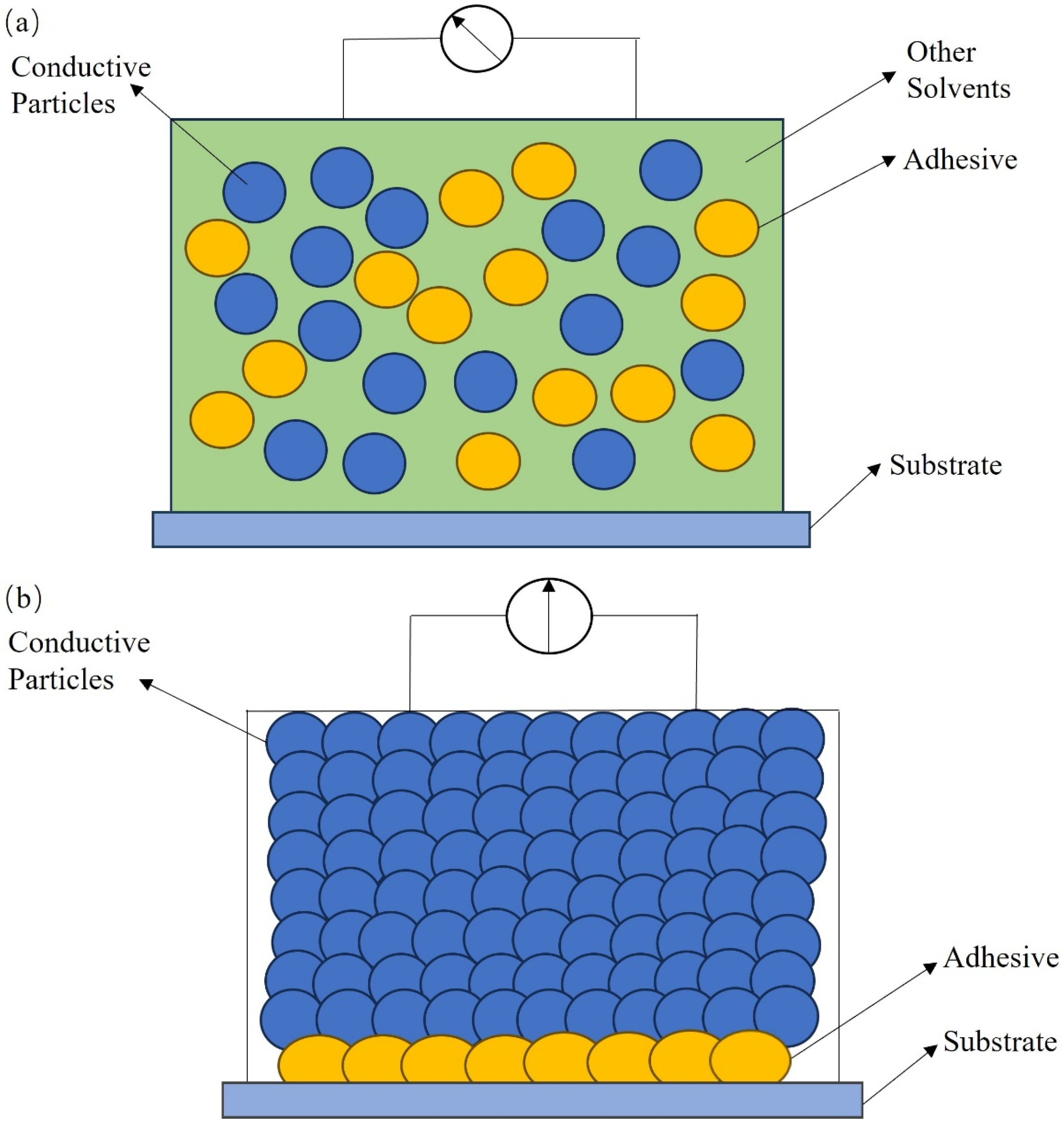
3.4. Composite Conductive Ink

Composite conductive ink is a kind of conductive ink prepared by combining the conductive functional phases of diverse systems or various characteristic materials in the same system. It is generally divided into carbon/metal composite conductive ink, carbon/polymer conductive ink, and conductive ink composed of different metals. Although the electrical properties of silver ink are excellent, the high cost limits its application in the manufacture of large-scale integrated circuits. In order to reduce the cost while improving their electrical properties, Li et al. employed an in situ reduction method to fabricate graphene-bridged silver conductive inks [25]. Cysteamine was chosen as the molecular bridging agent, with one end anchored to the graphene surface via the diazonium reaction and the other end linked to the silver atoms via the thiol functional group to achieve molecular-scale bridging between graphene and silver, thus facilitating the charge transfer at the graphene/silver interface, as demonstrated in Figure 8. The results revealed that the maximum conductivity of the prepared graphene-bridged silver conductive ink was capable of attaining 2 × 10⁵ S·m−1, and the printed circuit patterns exhibited high conductivity and excellent flexibility. Graphene could replace some of the silver nanoparticles and promote the longitudinal transfer of electrons between graphene and silver nanoparticles, enhancing the electrical conductivity while diminishing the amount of precious-metal silver and reducing the production cost.
Although graphene possesses high carrier mobility, the low carrier density is another intrinsic electrical property of graphene. In order to enhance the carrier density of graphene, chemical doping of graphene can make electrons transfer in or out of graphene to cause the generation of extra electrons/holes in graphene molecules, leading to n-type/p-type doping of graphene [51]. Therefore, Liu et al. achieved p-type doping of graphene with CuCl2 using the liquid-phase reaction method [52]. To prevent the agglomeration of graphene flakes through steric hindrance, polymers play a crucial role in graphene-based conductive ink by improving rheological properties and storage performance. In the subsequent preparation process, the composite conductive ink was prepared with the acquired CuCl2-doped graphene and carbon black as the composite conductive functional phase for retaining the polymers to possess excellent rheological properties, divalent acid ester (DBE) as the organic solvent, and polyurethane as the adhesive polymer, which achieved a conductivity of 3.13 × 10⁴ S·m−1 for the printed patterns. For the purpose of simplifying the preparation process, CuCl2 was directly added to the graphene conductive ink in the subsequent preparation process, and the same p-type doping of graphene in the ink system was achieved. Because carbon black was applied as an auxiliary conductive phase without removing polymers, the conductivity of printed patterns still attained 3.64 × 10⁴ S·m−1 with exceptional mechanical properties [26].
The reliable stability and extremely hydrophobic nature of graphene limit the application of water-based inks. The oxygenated groups of graphene oxide (GO) can effectively enhance its hydrophilicity and enable further chemical modification and functionalization, but the oxidation process damages its original structure and diminishes its electrical and mechanical properties. Restoring an extensive sp2 carbon network with excellent electrical properties while maintaining high hydrophilicity could be the appropriate functionalization approach in order to produce reduced graphene oxide (rGO) [53]. Giasafak et al. prepared carbon-based composite materials consisting of rGO and silver nanowires (AgNWs) through a physical mixture and an in situ reduction method [54]. The functionalization of the graphene sheets with amino and aryl sulfonic groups was achieved by adding 2,4-diaminobenzenesulfonic acid (DBSA) in the process of reduction, which could generate a positive effect on the electrical properties and water dispersibility. The mixing at the physical level allowed the AgNWs to be well dispersed and anchored onto the surface of rGO, resulting in a highly interconnected three-dimensional network that leads to enhanced surface conductivity. The in situ reduction method enabled the composite conductive inks to demonstrate better electrical properties. The conductivity of the conductive pattern prepared via the in situ reduction method could attain 7.4 × 10⁴ S·m−1. This is mainly attributed to the surface modification of AgNWs and graphene oxide by DBSA, which led to the covalent attachment on the surface of the rGO rather than surface adsorption in the physical mixture.
In contrast to the single-carbon-based conductive ink, the composite conductive phases were qualified to incorporate the advantages of various systems of conductive phases. By using approaches such as in situ reduction or chemical doping, more conductive channels can be constructed between metal conducting particles and graphene to enhance the electrical properties of conductive inks, while the introduction of polymers can effectively modify the rheological properties of the system to suit the electronic printing process. Through appropriate graphene oxidation and reduction processes, the hydrophilicity of graphene can be elevated for the preparation of aqueous conductive inks for more application areas, and its high conductivity can be maintained by preserving the sp2 carbon network structure. Meanwhile, the covalent attachment between rGO and other metal nanowires can effectively promote its overall electrical properties by constructing a three-dimensional conductive network. As a consequence, composite conductive ink provides superior electrical and thermal properties as well as high tensile strength and excellent resistance to electromigration, which can be an ideal choice for composite materials for integrated circuits. Therefore, composite conductive ink has enormous potential to be the material of first choice for the preparation of new electronic packaging materials, heat exchange materials of electronic components, and integrated circuit lead frames in the future.

4. Electronic Printing Technology for Conductive Ink

Conventional integrated circuit preparation usually involves photolithography, etching, or electroplating processing techniques. Photolithography requires high processing conditions and strict dust-free environments using expensive production facilities to produce integrated circuits. The preparation process is complicated, demanding the application of hazardous chemicals, making the IC manufacturing process time-consuming and costly. The electroplating procedure, regarded as the traditional circuit board (PCB) preparation technology, is both complicated and time-consuming. Moreover, the etching process consumes a lot of raw materials and requires the use of a large amount of acidic and corrosive liquids, which seriously pollute the environment. Electronic printing technology, without harsh environmental requirements and sophisticated manufacturing processes including photolithography, etching, and thin film deposition, is a newly emerging research direction within the field of integrated circuits [55]. Compared with photolithography and etching processing methods, electronic printing technologies not only greatly reduce the processing costs for integrated circuits but also are environmentally friendly. Conductive ink with high conductivity, oxidation resistance, and excellent mechanical properties frequently needs to be transferred to the corresponding circuit substrate using various electronic printing technologies to complete the printed preparation of integrated circuits. Distinct electronic printing approaches exert an essential influence on the circuit patterns, electrical properties, resolution, and other factors of the final integrated circuit. The electronic printing techniques routinely applied to prepare conductive inks for integrated circuits can be categorized into two main types: contact and noncontact. Contact printing mainly includes screen printing, gravure printing, and flexographic printing, and noncontact printing primarily consists of inkjet printing [56]. Table 2 summarizes the conductivities of commonly used conductive materials and the applicable printing techniques and curing processes.

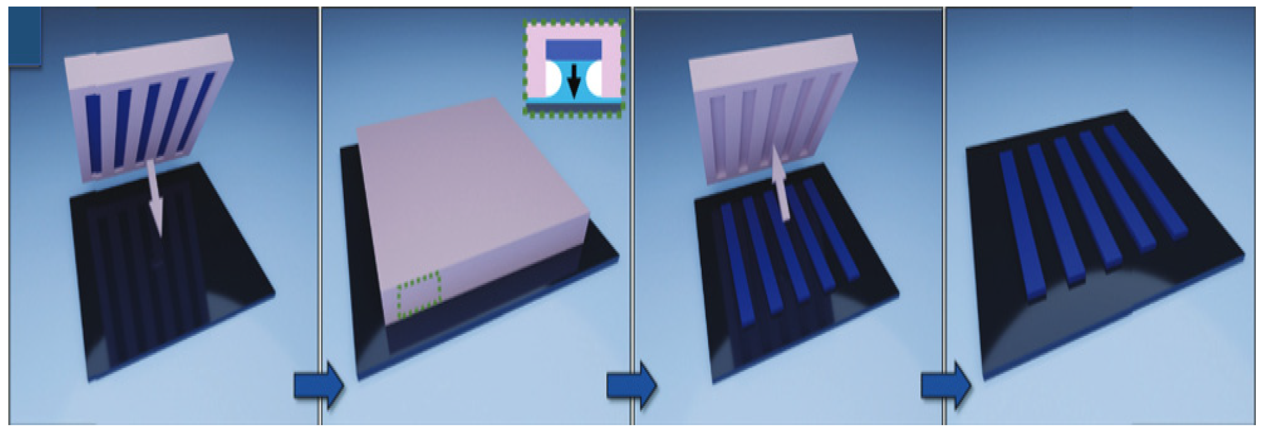
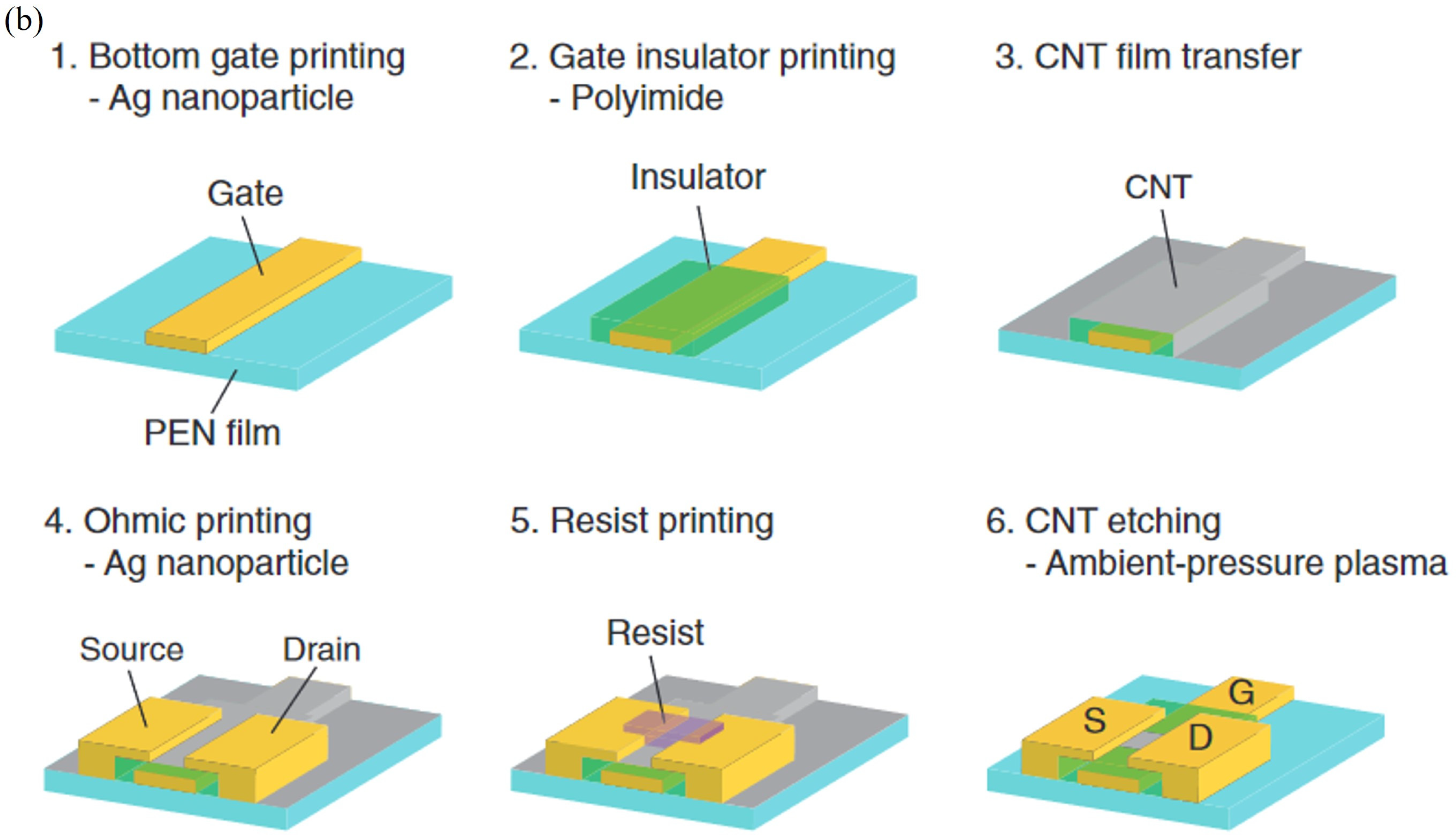
4.1. Screen Printing

Screen printing is a method in which ink only passes through the patterned part of a printing screen [57]. During the printing process, the ink is poured on the starting side of the screen without the circuit pattern, so that the ink will not leak through the screen. Afterward, a squeegee is applied to the ink with a certain amount of pressure while moving towards the other end of the screen at a uniform speed; the ink is squeezed through the patterned part of the screen to the substrate during the squeegee movement. Due to the low electrical conductivity of graphene oxide and the long preparation time required to prepare graphene from graphite using liquid-phase exfoliation, expanded graphite (EG) exhibits better dispersion than graphite because the van der Waals interactions are significantly weaker with the increased distance between the layers [58]. Kirill et al. produced well-dispersed and structurally intact graphene from expanded graphite using thermal expansion and high-shear-rate mixing measures. They obtained a graphene hybrid copolymer by applying polyvinylpyrrolidone (PVP) and polyvinyl acetate (PVAc) as bonding agents to achieve stabilization of the graphene gelation via steric hindrance of polymeric chains adsorbed on the surface of the graphene. They later replaced isopropyl alcohol with methyl ether of dipropylene glycol (DPM) using a solvent exchange approach to produce an environmentally friendly gel-like graphene conductive ink suitable for screen printing [59]. Due to the structural integrity of graphene facilitated by such a process and the presence of DPM solvent to adapt the rheological properties of the ink, graphene ink was screen printed and dried at 100 °C for 5 min to obtain a circuit pattern with a film conductivity of 1.3 × 10³ S·m−1 and a print resolution of 40 μm. Hyun et al. produced a graphene conductive ink by mixing graphene powder with ethyl cellulose (EC) and using ethanol and terpineol as solvents [60]. To increase the printing accuracy, a thin silicon wafer with a thickness of 90 μm, which was flexible enough to be employed for screen printing, was made as a screen-printing plate using a wet etching process. A circuit-printing template with a minimum opening width of only 5 μm was obtained on the silicon wafer using a photolithography process to achieve high-resolution patterns. An integrated circuit pattern with a high resolution of up to 40 μm and a conductivity of 1.86 × 10⁴ S·m−1 was achieved using screen printing, and the schematic diagram of the printing process is exhibited in Figure 9.
Table 2. A comparison of the electrical conductivities of several typical conductive inks.
Ink TypeComponentsPrinting TechniqueCuring MethodConductivityResolution
Metal [19]Copper nanoparticlesScreen printing250 °C/120 min5.9 × 106 S/m60 µm
Metal [27]Silver nanoparticlesAerosol jet printing180 °C/20 min4.3 × 106 S/m10 µm
Polymer [21]PEDOT: PSSDirect ink printing130 °C/30 min1.55 × 104 S/m30 µm
Carbon [22]GrapheneInkjet printing250 °C/30 min2.5 × 104 S/m40 µm
Carbon [23]GrapheneGravure printing250 °C/30 min104 S/m30 µm
Carbon [60]GrapheneScreen printing300 °C/30 min1.8 × 104 S/m40 µm
Composite [25]Graphene/AgDirect ink printing150 °C/30 min2 × 105 S/m/
Composite [26]Graphene/CuCl2Screen printing100 °C/15 min3.6 × 104 S/m/
The screen-printing process is quite convenient, as the resolution is consistently about tens of microns. Although it cannot satisfy the demands of printing high-resolution integrated circuits and processing precision electronic components, screen printing has outstanding viscosity adaptability of the ink. The accuracy of printed circuits can be further optimized by improving the accuracy of prefabricated stencils through lithography and etching processes. Moreover, the circuit production cost is affordable, with an expedient printing process, which is suitable for large-scale industrial production.

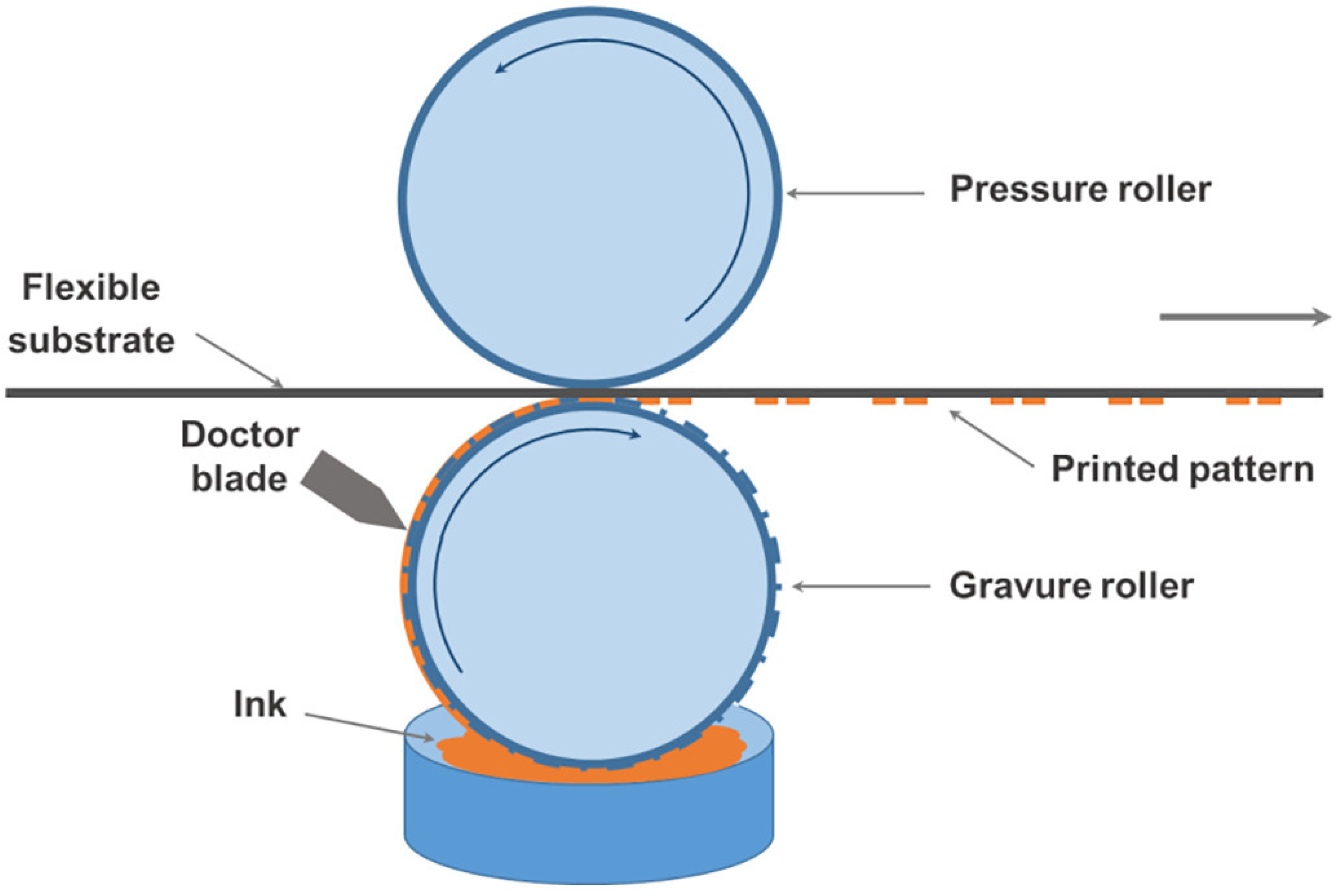
4.2. Gravure Printing

Gravure printing is a printing technique in which the graphic portion of the printing plate surface is recessed [61]. First, the conductive ink is spread all over the surface. Second, excess ink is scraped off using a doctor blade. Finally, the conductive ink is transferred to the substrate with greater pressure, as presented in Figure 10. This printing approach leads to a thicker ink layer, thereby yielding a finished product with high conductivity, providing a high-resolution conductive film layer as well as roll-to-roll deposition. Secor et al. dispersed graphene–EC powder in a mixture of ethanol and terpineol, which allowed rapid and complete dispersion [23]. By removing the ethanol to yield polymer-stabilized graphene in terpineol, which obtains ink with appropriate surface tension, the graphene ink can be applied for gravure printing. Continuous conductive lines were realized by increasing the viscosity of the ink and narrowing the spacing between the printing cells in the printing process. Continuous lines with 30 μm precise resolution and electrical conductivity of about 104 S·m−1 were achieved using such methods. In order to prepare environmentally friendly and low-cost water-based conductive inks for industrial gravure printing, Koutsioukis et al. employed an alternative solid phase 1,3 dipolar cycloaddition reaction to achieve functionalization of multiwalled carbon nanotubes (MWCNTs) with hydrophilic organic groups like catechols, which do not require the presence of organic solvents, resulting in fewer by-products and toxic solvent emissions, thus making the procedure more affordable and environmentally friendly [62]. The hydrophilic carbon nanotubes were then utilized to disperse the hydrophobic graphene nanosheets, and water-based styrene–acrylic and acrylic resins were used to prepare the water-based conductive inks for gravure printing [63]. 1,3 dipolar cycloaddition of azomethine ylide with MWCNTs could not only disperse graphene uniformly in water but also enhance the electrical conductivity of the MWCNT/graphene hybrid, leading to conductivity values via gravure printing of up to 3.125 × 10⁴ S·m−1.
In conclusion, by increasing the viscosity of the ink and narrowing the spacing between the printing cells, the printing resolution can be further elevated. With the development of environmentally friendly, highly conductive carbon-based inks, the promotion and application of gravure printing in more electronic components and conductive patterns can be broadened. In addition, gravure printing is also capable of providing high printing speeds and is suitable for large-scale, high-rate printing of integrated circuits.

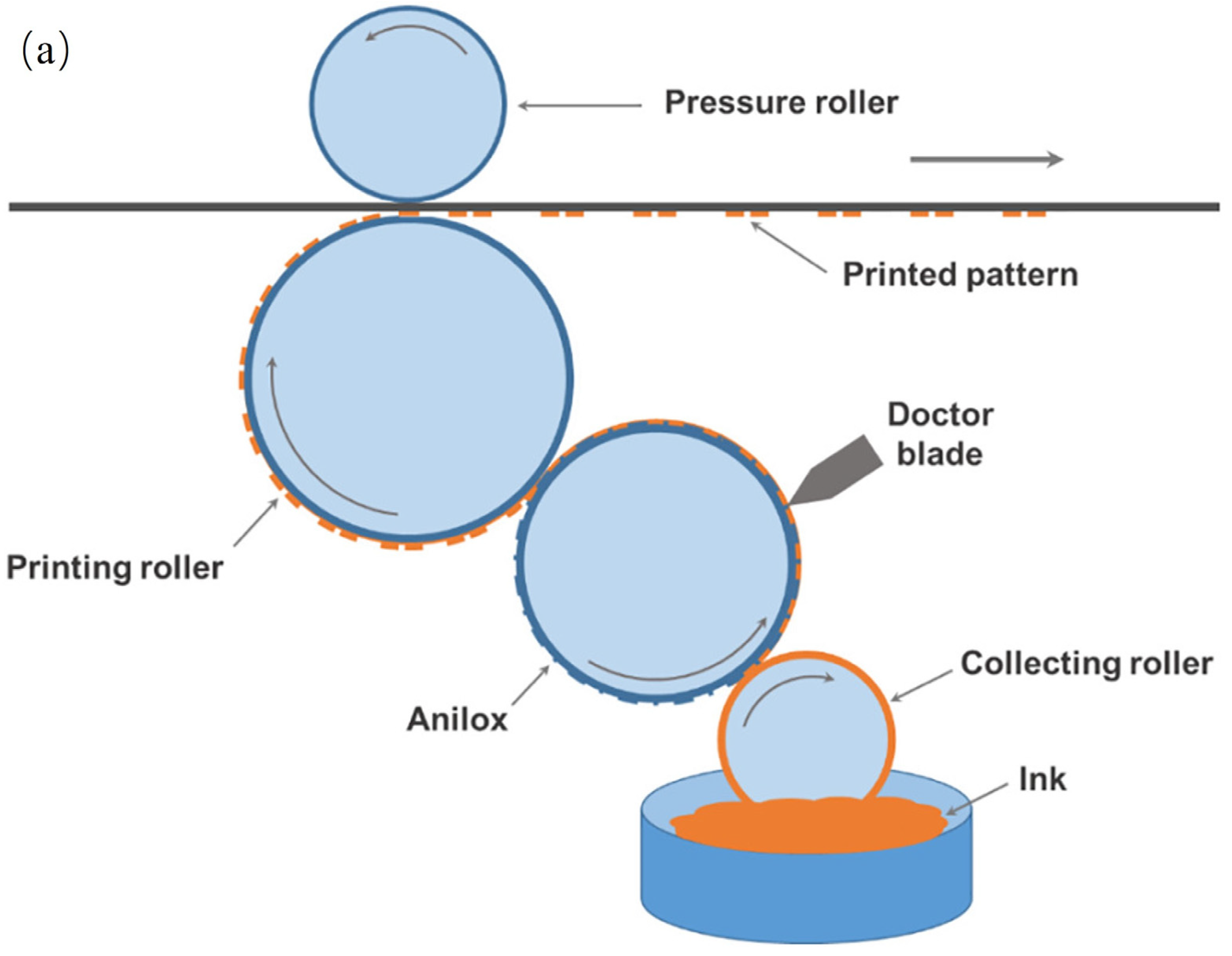
4.3. Flexographic Printing

Relief printing, also known as flexographic printing, is a promising roll-to-roll manufacturing technique similar to gravure printing, except that the printing rolls generally consist of rubber or polymeric materials. A representative flexographic printing system includes four rollers, as displayed in Figure 11a. The ink is gathered by a collection cylinder and transferred onto anilox rollers (rollers with engraved patterns). The conductive ink adheres to the circuit pattern on the anilox rollers, with excess ink being scraped away by a doctor blade. The printed circuit pattern is subsequently transferred to the substrate through the printing roller [65]. This direct-contact printing process benefits from printing rollers composed of rubber (or polymer) that are more flexible, which diminishes the impact of the printing rollers on the conductive film, thus minimizing creases and scratches on the substrate. The process is straightforward and industrially scalable, making it ideal for the printing of flexible conductive films, flexible integrated circuits, and electronic components. Higuchi et al. fabricated high-mobility thin film field effect transistors (TFTs) using carbon nanotubes (CNTs) via the flexographic printing technique. Three inks were manipulated during the preparation: (1) Ag ink to generate the gate, source, and drain; (2) polyimide (PI) ink to shape the gate insulator; and (3) resist ink to model the CNTs [66]. CNT films were fabricated using gas-phase filtration and transfer techniques [67]. The process flow of the TFT device manufacturing is shown in Figure 11b. Outstanding quality CNTs are essential in obtaining high-mobility TFTs with 157 cm2 V−1 s−1 because they decrease the number of intertube junctions, which usually have high contact resistance along the pathway. Owing to the roll-to-roll manufacturing process, flexographic printing with high printing speed can be applied to the large-area manufacturing of transistors and combined with inks with different characteristics; it is also anticipated to be utilized in the processing of flexible electronic devices, RFIDs, and other electronic devices.

4.4. Inkjet Printing

Inkjet printing is a drop-on-demand, noncontact material jetting technology in which conductive ink is deposited onto the surface of a circuit substrate at high speed under pressure through a specially designed nozzle. The conductive ink is printed directly under computer control to produce the desired circuit pattern without the necessity of fabricating a printing template in advance or shaping the circuit pattern through etching. The viscosity of conductive ink used for inkjet printing is supposed to be controlled at around 2~25 mPa·s [68]. Because the ink viscosity is greater than 40 mPa·s, it makes the inkjet printing process difficult at room temperature. An ink that flows properly with a low viscosity of 2~25 mPa·s will not accumulate at the nozzle, block the nozzle, or cause the ink droplets to deviate from the predefined trajectory. Htwe et al. prepared water-based graphene conductive ink using graphene, surfactant PVP, and deionized water (DI) using ultrasonic dispersion [69]. The fabrication process of inkjet printing a conductive pattern is illustrated in Figure 12b. PVP chains can be grafted via monomer copolymerization or free radical grafting, thus maintaining tight bonds with graphene sheets, which contributes to the dispersion stability of graphene sheets. The polar hydrophilic group of the pyrrolidone ring has a powerful affinity for water, which can increase the degree of water penetration into the graphene sheets. Using multiple printing cycles of inkjet printing, the gaps between the conductive paths of the graphene sheets can be effectively narrowed and the void structure in the system reduced, thus resulting in enhanced conductivity of 5.2 × 10³ S·m−1. The manufacturing process for electronic devices also has significant requirements for print resolution. Conventional inkjet printing technology has limited printing accuracy, with printing resolutions of up to 40 microns or more. In order to form high-density components in integrated circuits, it is essential to ensure that the minimum size of the structure is in the range of 10 to 30 μm. Aerosol inkjet printing has evolved from inkjet printing technology to improve printing accuracy. Aerosol inkjet printing enables the formation of functional microstructures with lateral dimensions of 10 microns on a variety of substrates, facilitating the formation of high-density components in integrated circuits [70]. To ensure the aggregation stability of the nanoparticles, Arsenov used the low-toxicity solvents ethylene glycol and water [71]. Platinum nanoparticles obtained using the spark discharge method can be utilized to fabricate highly conductive functional nano-inks. PVP was used as a bonding additive and binder for platinum nano-inks. To be adaptable to an aerosol inkjet printing system, a platinum conductive ink with a solid content of 25 percent and a viscosity of 11 mPa·s was configured. Prepared platinum nano-inks are an excellent solution for the formation of narrow (up to 30 µm) and highly conductive platinum lines using an aerosol jet printing system. The conductivity of a platinum wire sintered at 750 °C is 8.3 × 10⁶ S·m−1. The ink preparation and aerosol inkjet printing process are illustrated in Figure 12c. In the aerosol inkjet printing process, the use of highly volatile solvents can enhance the atomization of conductive inks, but it still leads to excessive aerosol flow and droplet dryness, resulting in turbulence and overspray. Hung et al. utilized propylene glycol monomethyl ether (PGME) and ethylene glycol (EG) with different volatility rates as mixed solvents with a 1:4 addition ratio. Hung prepared silver conductive inks using silver nanoparticles with an average particle size of 100 nm (60% solids) and mixed solvents to successfully print high-quality conductive circuits [27]. The conductivity of printed circuits up to 4.3 × 10⁶ S·m−1 and 4B adhesion after the curing process at 180 °C was achieved. Jabari et al. dispersed 40 mg/mL of graphene and ethyl cellulose powder in a mixed solvent of ethanol and turpentine alcohol (ratio 97.5:2.5), filtered it through a filter to obtain the dispersion, and mixed the dispersion with silver nanoparticle solution in a 1:3 volume ratio to configure a stable graphene/silver conductive ink [72]. Through an aerosol inkjet printing process and after sintering at 250 °C for 30 min, a uniform microstructure and crack-free graphene/silver conductive patterns with good conductivity and flexibility were obtained, exhibiting the prospect of aerosol inkjet printing technology for flexible electronics applications. Certainly, inkjet printing technology is only one type of 3D printing technology. Other 3D printing technologies such as direct ink writing (DIW) and fused deposition modeling (FDM) are also used to print circuits. Huk et al. invented a high-performance printable ink using advanced DIW printing techniques [21]. In order to achieve favorable rheological properties for a DIW printing technique, this ink was based on a cryogenically frozen aqueous solution of PEDOT:PSS, which was then lyophilized and subjected to controlled redispersion in a mixture of water and dimethyl sulfoxide (DMSO). The resulting conductive polymer ink had excellent 3D printing properties and was capable of high resolution (over 30 microns) as well as high conductivity (up to 1.55 × 10⁴ S·m−1). Zhang et al. synthesized highly conductive graphene with conductivity of up to 6 × 10⁴ S·m−1 using a modified two-step in situ reduction method [73]. The PLA and graphene were mixed homogeneously via melting so that the graphene was well dispersed in the PLA substrate. The composite material was then processed into a composite filament with a diameter of 1.75 mm. Due to the fact that the filament used for the FDM technique was made via melt extrusion, the filament can be smoothly extruded from the nozzle. Two-dimensional and three-dimensional flexible circuits can be printed on different substrates using FDM technology. The composite circuits exhibited strong interfacial bonding with the substrate and had conductivity values of up to 4.76 × 10² S/m.
To summarize, inkjet printing has the advantages of not needing the mask plate to be prefabricated in advance, being able to directly print complex circuit patterns, saving raw materials, and printing at a fast speed. The viscosity of the ink used for inkjet printing must be kept within a certain range; otherwise, nozzle clogging, leakage, and other problems are likely. Among the many technologies of inkjet printing, aerosol inkjet printing can enhance the circuit printing accuracy to 10 microns and can be widely used in various types of rigid and flexible substrates. In addition, DIW and FDM printing technologies are also being used to print integrated circuits. Three-dimensional printing technology further expands the diversity of electronic printing technologies and provides more processing methods for the manufacturing of integrated circuits.

5. Conclusions

With various advanced electronic printing technologies, conductive ink can be utilized for the preparation of conductive films, flexible electronic components, transistors, chip packaging, large-scale integrated circuits, and other electronic products. The main inferences are presented below.
(1)
The newly created carbon conductive ink demonstrates the advantages of electrical conductivity, thermal conductivity, oxidation resistance, etc. The agglomeration problem of carbon conductive ink was solved by adding surfactant molecules and adjusting the composition of the solvent. In order to increase the hydrophilicity and the electrical conductivity of carbon-based ink, aromatic polymers and conjugated conductive polymers can be used in the preparation of graphene. Carbon-based composite conductive inks are considered to be the most prospective conductive inks; they combine the advantages of diverse systems of conductive materials.
(2)
Screen printing is suitable for large-scale production with printing accuracy. Gravure printing and flexographic printing are more adaptable for the manufacture of large-area flexible integrated circuits. Inkjet printing is more applicable for the manufacture of high-precision integrated circuits. These printing technologies can make up for the limitations of traditional photolithography and electroplating processes, thereby further broadening their application in various electronic products.
(3)
Conductive inks and electronic printing technologies are complementary to each other. The development of carbon-based composite conductive inks demonstrates outstanding conductive and printing performance. It will lead to the fabrication of large-scale integrated circuits in the future with the advantages of more precise printing accuracy, faster printing speed, and lower production cost.

Author Contributions

Conceptualization, Y.Q. and S.W.; resources, Y.L., W.L., Q.L. and Y.Q.; writing—original draft preparation, Y.Q., S.W. and X.O.; writing—review and editing, S.W., Y.Q. and X.O.; visualization, Y.Q. and S.W.; supervision, S.W.; project administration, S.W.; funding acquisition, S.W. All authors have read and agreed to the published version of the manuscript.

Funding

This work was supported by the Key Research Project of the Education Department of Guangdong Province in China (No. 2020ZDZX2026) and the Science and Technology Plan of Guangdong Province in China (No. STKJ2023070).

Institutional Review Board Statement

Not applicable.

Informed Consent Statement

Not applicable.

Data Availability Statement

All data supporting the conclusions of this manuscript are included within the manuscript.

Conflicts of Interest

The authors declare no conflict of interest.

References

  1. Yan, Y.K.; Zhao, Y.; Liu, Y.Q. Recent progress in organic field-effect transistor-based integrated circuits. J. Polym. Sci. 2022, 60, 311–327. [Google Scholar] [CrossRef]
  2. Htwe, Y.Z.N.; Mariatti, M. Printed graphene and hybrid conductive inks for flexible, stretchable, and wearable electronics: Progress, opportunities, and challenges. J. Sci. Adv. Mater. Devices 2022, 7, 100435. [Google Scholar] [CrossRef]
  3. Li, W.W.; Zhang, H.R.; Kagita, S.; Shamim, A. All screen-printed, polymer-nanowire based foldable electronics for mm-wave applications. Adv. Mater. Technol. 2021, 6, 2100525. [Google Scholar] [CrossRef]
  4. Knapp, H.; Romagnoil, G. RFID systems optimization through the use of a new network planning algorithm to support the design of receiving gates. J. Intell. Manuf. 2023, 34, 1389–1407. [Google Scholar] [CrossRef]
  5. Jost, N.; Askins, S.; Dixon, R.; Ackermann, M.; Dominguze, C.; Anton, I. Array of micro multijunction solar cells interconnected by conductive inks. Sol. Energy Mater. Sol. Cells 2022, 240, 111693. [Google Scholar] [CrossRef]
  6. Hong, H.; Jiang, L.H.; Tu, H.T.; Hu, J.Y.; Moon, K.S.; Yan, X.; Wong, C.P. Rational design and evaluation of UV curable nano-ink applied in highly conductive textile-based electrodes and flexible silver-zinc batteries. J. Mater. Sci. Technol. 2022, 101, 294–307. [Google Scholar] [CrossRef]
  7. Cinquino, M.; Prontera, C.T.; Zizzari, A.; Giuri, A.; Pugllese, M.; Giannuzzi, R.; Monteduro, A.G.; Carugati, M.; Banfi, A.; Carallo, S. Effect of surface tension and drying time on inkjet-printed PEDOT:PSS for ITO-free OLED devices. J. Sci. Adv. Mater. Devices 2022, 7, 100394. [Google Scholar] [CrossRef]
  8. Sim, I.; Park, S.; Shin, K.Y.; Yang, C.; Kang, H.; Hwang, J.Y.; Moon, S.J. Inkjet printing of high aspect ratio silver lines via laser-induced selective surface wetting technique. Coatings 2023, 13, 683. [Google Scholar] [CrossRef]
  9. Wu, K.B.; Tang, X.W.; An, E.J.; Yun, Y.H.; Kim, S.J.; Moon, S.H.; Kong, H.Y.; Kim, S.H.; Jeong, Y.J. Screen printing of graphene-based nanocomposite inks for flexible organic integrated circuits. Org. Electron. 2022, 108, 106603. [Google Scholar] [CrossRef]
  10. Hines, H.R.; Gu, Y.; Martin, A.A.; Li, P.; Fleischer, J.; Clough-Paze, A.; Stackhouse, G.; Dasgupta, A.; Das, S. Considerations of aerosol-jet printing for the fabrication of printed hybrid electronic circuits. Addit. Manuf. 2021, 47, 102325. [Google Scholar] [CrossRef]
  11. Dimitriou, E.; Michailidis, N. Printable conductive inks used for the fabrication of electronics: An overview. Nanotechnology 2022, 32, 502009. [Google Scholar] [CrossRef] [PubMed]
  12. Liu, P.; He, W.Q.; Lu, A.X. Preparation of low temperature sintered high conductivity inks based on nano silver self-assembled on surface of graphene. J. Cent. South Univ. 2022, 26, 2953–2960. [Google Scholar] [CrossRef]
  13. Toledo, D.; Cristofolini, I.; Molinari, A.; Arnhold, V.; Kruzhanov, V.; Vervoort, P.; Dougan, M.; Wibert, L.; Bonnefoy, V.; Hellein, R.; et al. High temperature sintering and its effect on dimensional and geometrical precision and on microstructure of low alloyed steels. Powder Metall. 2020, 63, 80–93. [Google Scholar] [CrossRef]
  14. Geng, X.; Hong, Y.Z.; Lei, J.C.; Ma, J.X.; Chen, J.; Xiao, H.; Tong, J.H.; Bordia, R.K.; Peng, F. Ultra-fast, selective, non-melting, laser sintering of alumina with anisotropic and size-suppressed grains. J. Am. Ceram. Soc. 2021, 104, 1997–2006. [Google Scholar] [CrossRef]
  15. Tang, J.Y.; Mak, C.H.H.; Tam, S.K.; Ng, K.M. Formulation of a paste for copper thick film. J. Nanopart. Res. 2021, 23, 166. [Google Scholar] [CrossRef]
  16. Green, A.A.; Hersam, M.C. Colored semitransparent conductive coatings consisting of monodisperse metallic single-walled carbon nanotubes. Nano Lett. 2008, 8, 1417–1422. [Google Scholar] [CrossRef]
  17. Seager, C.H.; Pike, G.E. Percolation and conductivity: A computer study I and II. Phys. Rev. B. 1974, 10, 1421–1446. [Google Scholar] [CrossRef]
  18. Jiao, J.; Yao, J.Y. Functional Polymer Materials, 2nd ed.; Chemical Industry Press: Beijing, China, 2016; pp. 114–124. [Google Scholar]
  19. Chen, C.L. Research on Synthesis, Sintering and Application of Copper Nanoparticles Used for Printed Electronics. Master’s Thesis, Huazhong University of Science and Technology, Wuhan, China, 2017. [Google Scholar]
  20. Corletto, A.; Shapter, J.G. High-resolution and scalable printing of highly conductive PEDOT: PSS for printable electronics. J. Mater. Chem. C. 2021, 9, 14161. [Google Scholar] [CrossRef]
  21. Yuk, H.; Lu, B.Y.; Lin, S.; Qu, K.; Xu, J.K.; Luo, J.H.; Zhao, X.H. 3D printing of conducting polymers. Nat. Commun. 2020, 11, 1604. [Google Scholar] [CrossRef]
  22. Secor, E.B.; Prabhumirashi, P.L.; Puntambekar, K.; Geier, M.L.; Hersam, M.C. Inkjet printing of high conductivity, flexible graphene patterns. J. Phys. Chem. Lett. 2013, 4, 1347–1351. [Google Scholar] [CrossRef]
  23. Secor, E.B.; Lim, S.; Zhang, H.; Frisbie, C.D.; Francis, L.F.; Hersam, M.C. Gravure printing of graphene for large-area flexible electronics. Adv. Mater. 2014, 26, 4533–4538. [Google Scholar] [CrossRef] [PubMed]
  24. Tran, T.S.; Balu, R.; Campo, L.D.; Dutta, N.K.; Choudhury, N.R. Sulfonated polythiophene-interfaced graphene for water redispersible graphene powder with high conductivity and electrocatalytic activity. Energy Adv. 2023, 2, 365–374. [Google Scholar] [CrossRef]
  25. Li, W.X.; Yan, J.M.; Wang, C.; Zhang, N.; Choy, T.H.; Liu, S.; Zhao, L.; Tao, X.M.; Chai, Y. Molecule bridged graphene/Ag for highly conductive ink. Sci. China Mater. 2022, 65, 2771–2778. [Google Scholar] [CrossRef]
  26. Liu, L.X.; Zhang, X.J.; Ma, H.; Shen, Z.G. CuCl2-doped graphene-based screen printing conductive inks. Sci. China Mater. 2022, 65, 1890–1901. [Google Scholar] [CrossRef]
  27. Hung, K.Y.; Chang, Y.T.; Chien, C.H.; Ding, C.F.; Tsai, M.C.; Young, H.T. Investigation of ink modification for aerosol jet printing process on FR-4 substrate. Int. J. Adv. Manuf. Technol. 2020, 111, 1147–1156. [Google Scholar] [CrossRef]
  28. Simmons, J.G. Generalized formula for the electric tunnel effect between similar electrodes separated by a thin insulting film. J. Appl. Phys. 1963, 34, 1793–1803. [Google Scholar] [CrossRef]
  29. Beek, L.K.H.V.; Pu, B.I.C.F.V. Field emission in carbon black-loaded natural rubber vulcanizates. J. Appl. Polym. Sci. 1963, 6, 651–655. [Google Scholar] [CrossRef]
  30. Zhan, H.J.; Guo, J.Y.; Yang, X.Z.; Guo, B.; Liu, W.; Shen, H.Y.; Wang, X.R.; Tang, W.G.; Chen, F. Silver frameworks based on self-sintering silver micro flakes and its applications in low temperature curing. J. Mater. Sci. Mater. Electron. 2019, 30, 21343. [Google Scholar] [CrossRef]
  31. Zareel, A.; Gopalakrishnan, S.; Mutlu, Z.; He, Z.H.; Peana, S.; Wang, H.Y.; Rahimi, R. Highly conductive copper-silver bimodal for low-cost printed electronics. ACS Appl. Electron. Mater. 2019, 3, 3352–3364. [Google Scholar] [CrossRef]
  32. Mo, L.X.; Guo, Z.X.; Yang, L.; Zhang, Q.Q.; Fang, Y.; Xin, Z.Q.; Chen, Z.; Hu, K.; Han, L.; Li, L.H. Silver nanoparticles based ink with moderates sintering in flexible and printed electronics. Int. J. Mol. Sci. 2019, 20, 2124. [Google Scholar] [CrossRef]
  33. Zhang, Y.; Qi, S.H.; Wu, X.M.; Duan, G.C. Electrically conductive adhesive based on acrylate resin filled with silver plating graphite nanosheet. Synth. Met. 2011, 161, 516. [Google Scholar] [CrossRef]
  34. Min, H.; Lee, B.; Jeong, S.; Lee, M. Fabrication of 10 mu m-scale conductive Cu patterns by selective laser sintering of Cu complex ink. Opt. Laser Technol. 2017, 88, 128–133. [Google Scholar] [CrossRef]
  35. Hwang, H.J.; Oh, K.H.; Kim, H.S. All-photonic drying and sintering process via flash white light combined with deep-UV and near-infrared irradiation for highly conductive copper nano-ink. Sci. Rep. 2016, 6, 19696. [Google Scholar] [CrossRef]
  36. Del, L.C.; Zinn, A.A.; Ruch, P.; Bouville, F.; Studart, A.R.; Brunschwiler, T. Oxide-free copper pastes for the attachment of large-area power devices. J. Electron. Mater. 2019, 48, 6823–6834. [Google Scholar]
  37. Mou, Y.; Liu, J.X.; Cheng, H.; Peng, Y.; Chen, M.X. Facile preparation of self-reducible Cu nanoparticle paste for low temperature Cu-Cu Bonding. JOM 2019, 71, 3076–3083. [Google Scholar] [CrossRef]
  38. Li, J.J.; Liang, Q.; Chen, C.; Shi, T.L.; Liao, G.L.; Tang, Z.R. Cu-Cu bonding by low-temperature sintering of self-healable Cu nanoparticles. In Proceedings of the 2019 IEEE 69th Electronic Components and Technology Conference, Las Vegas, NV, USA, 28–31 May 2019. [Google Scholar]
  39. Acherjee, B. State-of-art review of laser irradiation strategies applied to laser transmission welding of polymers. Opt. Laser Technol. 2021, 137, 106737. [Google Scholar] [CrossRef]
  40. Hu, Z.R.; Dai, R.; Wang, D.N.; Wang, X.N.; Chen, F.; Fan, X.L.; Chen, C.J.; Liao, Y.L.; Nian, Q. Preparation of graphene/copper nanocomposites by ball milling followed by pressureless vacuum sintering. New Carbon Mater. 2021, 36, 420–428. [Google Scholar] [CrossRef]
  41. Pang, H.; Xu, L.; Yan, D.X.; Li, Z.M. Conductive polymer composites with segregated structures. Prog. Polym. Sci. 2014, 39, 1908–1933. [Google Scholar] [CrossRef]
  42. Zen, H.; Zhang, S.H.; Xie, Y.; Jiang, H.Y.; Li, M.C. Preparation and printability of polythiophene-based conductive inks. Packag. J. 2019, 11, 58–67. [Google Scholar]
  43. Wang, Z.W.; Cui, H.J.; Li, S.; Feng, X.W.; Aghassi, J.H.; Azizian, S.; Levkin, P.A. Facile approach to conductive polymer microelectrodes for flexible electronics. ACS Appl. Mater. Interfaces 2021, 13, 21661–21668. [Google Scholar] [CrossRef]
  44. Novoselov, K.S.; Geim, A.K.; Morozvo, S.V.; Jiang, D.; Zhang, Y.; Dubonos, S.V.; Grigorieva, I.V.; Firsov, A.A. Electric field effect in atomically thin carbon films. Science 2004, 306, 666–669. [Google Scholar] [CrossRef] [PubMed]
  45. Lee, C.; Wei, X.D.; Kysar, J.W.; Hone, J. Measurement of the elastic properties and intrinsic strength of monolayer graphene. Science 2008, 321, 385. [Google Scholar] [CrossRef]
  46. Shin, K.W.; Cho, Y.C.; Nam, S.G.; Jung, A.L.; Lee, E.K.; Lee, C.S.; Lee, M.H.; Shin, H.J.; Byun, K.E. Graphene capping of Cu back-end-of-line interconnects reduces resistance and improves electromigration lifetime. ACS Appl. Nano Mater. 2023, 6, 4170–4177. [Google Scholar] [CrossRef]
  47. Gao, Y.H.; Shi, W.; Wang, W.C.; Leng, Y.P.; Zhao, Y.P. Inkjet printing patterns of highly conductive pristine graphene on flexible substrates. Ind. Eng. Chem. Res. 2014, 53, 16777–16784. [Google Scholar] [CrossRef]
  48. Tran, T.S.; Balu, R.; Nguyen, C.K.; Mata, J.; Truong, V.K.; Dutta, N.K.; Choudhury, N.R. Graphene nanosheets stabilized by P3HT nanoparticles for printable metal-free electrocatalysts for oxygen reduction. ACS Appl. Nano Mater. 2023, 6, 908–917. [Google Scholar] [CrossRef]
  49. Lin, M.Y. Preparation of PristineGraphene Conductive Paste for Screen Printing and Its Applications. Master’s Thesis, Shanghai Jiao Tong University, Shanghai, China, 2019. [Google Scholar]
  50. Qi, C.L. Slurry of Carbon Nanotubes as Conductive Addictive for Lithium Batteries. Master’s Thesis., China University of Petroleum, Beijing, China, 2016. [Google Scholar]
  51. Arsie, L.; Esconjauregui, S.; Weatherup, R.; Guo, Y.Z.; Bhardwaj, S.; Centeno, A.; Zurutuza, A.; Cepek, C.; Robertson, J. Stability of graphene doping with MoO3 and I2. Appl. Phys. Lett. 2014, 105, 103103. [Google Scholar] [CrossRef]
  52. Singh, A.K.; Ahmad, M.; Singh, V.K.; Shin, K.; Seo, Y.; Eom, J. Tailoring the electrical properties of graphene layers by molecular doping. ACS Appl. Mater. Interfaces 2013, 5, 5276–5281. [Google Scholar] [CrossRef]
  53. Barmpakos, D.; Belessi, V.; Schelwald, R.; Kaltaas, G. Evaluation of inkjet-printed reduced and functionalized water-dispersible graphene oxide and graphene on polymer substrate—Application to printed semperature Sensors. Nanomaterials 2021, 11, 2025. [Google Scholar] [CrossRef]
  54. Giasafaki, D.; Mitzithra, C.; Belessi, V.; Filippakopoulou, T.; Koutsioukis, A.; Georgakilas, V.; Charalambopoulou, G.; Steriotis, T. Graphene-based composites with silver nanowires for electronic applications. Nanomaterials 2022, 12, 3443. [Google Scholar] [CrossRef]
  55. Assaifan, A.K. Flexographic Printing Contributions in Transistors Fabrication. Adv. Eng. Mater. 2021, 23, 2001410. [Google Scholar] [CrossRef]
  56. Tong, S.C.; Sun, J.; Yang, J.L. Printed thin-film transistors: Research from China. ACS Appl. Mater. Interfaces 2018, 10, 25902–25924. [Google Scholar] [CrossRef] [PubMed]
  57. Wang, H.X.; Qian, J.; Li, H.B.; Ding, F.Y. Rheological characterization and simulation of chitosan-TiO2 edible ink for screen-printing. Prog. Org. Coat. 2018, 120, 19–27. [Google Scholar] [CrossRef]
  58. Shih, C.J.; Vijayaraghavan, A.; Krishnan, R.; Sharma, R.; Han, J.H.; Ham, M.H.; Jin, Z.; Lin, S.C.; Paulus, G.L.C.; Reuel, N.F.; et al. Bi- and trilayer graphene solutions. Nat. Nanotechnol. 2011, 6, 439–445. [Google Scholar] [CrossRef] [PubMed]
  59. Arapov, K.; Rubingh, E.; Abble, R.; Laven, J.; de With, G.; Friedrich, H. Conductive screen printing inks by gelation of graphene dispersions. Adv. Funct. Mater. 2016, 26, 586–593. [Google Scholar] [CrossRef]
  60. Hyun, W.J.; Secor, E.B.; Hersam, M.C.; Frisbie, C.D.; Francis, L.F. High-resolution patterning of graphene by screen printing with a silicon stencil for highly flexible printed electronics. Adv. Mater. 2015, 27, 109–115. [Google Scholar] [CrossRef]
  61. Sico, G.; Montanino, M.; Del Mauro, A.D.; Imparato, A.; Nobile, G.; Minarni, C. Effects of the ink concentration on multi-layer gravure-printed PEDOT: PSS. Org. Electron. 2016, 28, 257–262.-5448. [Google Scholar] [CrossRef]
  62. Georgakilas, V.; Demeslis, A.; Ntararas, E.; Kouloumpis, A.; Dimos, K.; Gournis, D.; Zboril, R. Hydrophilic nanotube supported graphene–water dispersible carbon superstructure with excellent conductivity. Adv. Funct. Mater. 2015, 25, 1481–1487. [Google Scholar] [CrossRef]
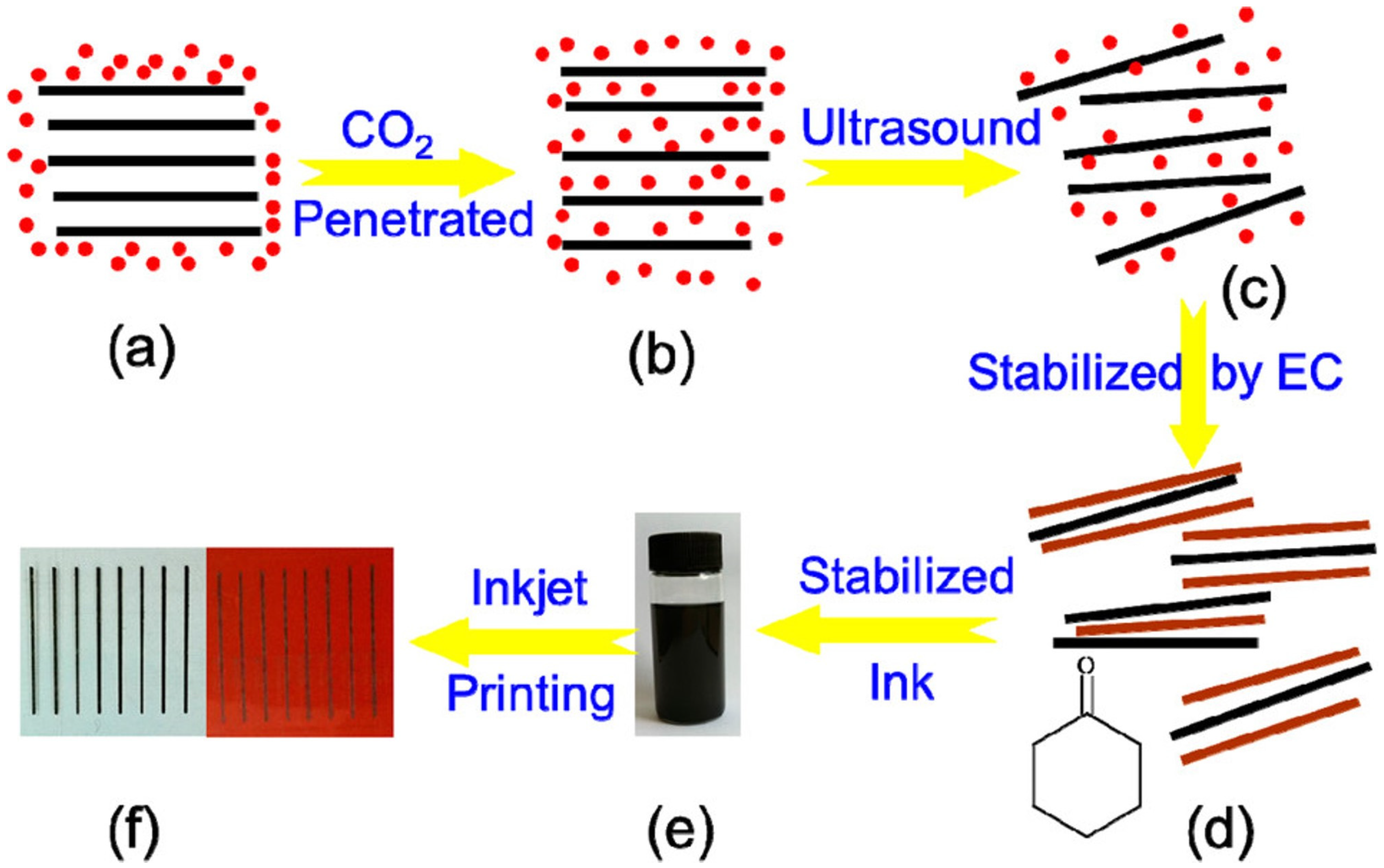
  63. Koutsioukis, A.; Belessii, V.; Georgkilas, V. Solid phase functionalization of MWNTs: An eco-friendly approach for carbon-based conductive inks. Green Chem. 2021, 23, 5442–5448. [Google Scholar] [CrossRef]
  64. Tran, T.S.; Dutta, N.K.; Choudhury, N.R. Graphene inks for printed flexible electronics: Graphene dispersions, ink formulations, printing techniques and applications. Adv. Colloid Interface Sci. 2018, 261, 41–61. [Google Scholar] [CrossRef]
  65. Qu, Y.F.; Wang, Q.; Dai, H.Q. Research progress of graphene and its composite ink used in flexible printing electronics. J. Funct. Mater. 2020, 51, 11031–11041. [Google Scholar]
  66. Higuchi, K.; Kishimoto, S.; Nakajima, Y.; Tomura, T.; Takesue, M.; Hata, K.; Kauppinen, E.I.; Ohno, Y. High-mobility, flexible carbon nanotube thin-film transistors fabricated by transfer and high-speed flexographic printing techniques. Appl. Phys. Express 2013, 6, 085101. [Google Scholar] [CrossRef]
  67. Sun, D.M.; Timmermans, M.Y.; Tian, Y.; Nasibulin, A.G.; Kauppinen, E.I.; Kishimoto, S.; Mizutani, T.; Ohno, Y. Flexible high-performance carbon nanotube integrated circuits. Nat. Nanotechnol. 2011, 6, 156–161. [Google Scholar] [CrossRef]
  68. Aleeva, Y.; Pignataro, B. Recent advances in upscalable wet methods and ink formulations for printed electronics. J. Mater. Chem. C. 2014, 2, 6436–6453. [Google Scholar] [CrossRef]
  69. Htwe, Y.Z.N.; Mariatti, M. Surfactant-assisted water-based graphene conductive inks for flexible electronic applications. J. Taiwan Inst. Chem. Eng. 2021, 125, 402–412. [Google Scholar] [CrossRef]
  70. Rosker, E.S.; Barako, M.T.; Nguyen, E.; Dimarzio, D.; Kisslinger, K.; Duan, D.W.; Sandhu, R.; Goorsky, M.S.; Tice, J. Approaching the practical conductivity limits of aerosol jet printed silver. ACS Appl. Mater. Interfaces 2020, 12, 29684–29691. [Google Scholar] [CrossRef]
  71. Arsenov, P.V.; Efimov, A.A.; Ivanov, V.V. Optimizing aerosol jet printing process of platinum ink for high-resolution conductive microstructures on ceramic and polymer substrates. Polymers 2021, 13, 918. [Google Scholar] [CrossRef]
  72. Jabari, E.; Toyserkani, E. Aerosol-jet printing of highly flexible and conductive graphene/silver patterns. Mater. Lett. 2016, 174, 40–43. [Google Scholar] [CrossRef]
  73. Zhang, D.; Chi, B.H.; Li, B.W.; Gao, Z.W.; Du, Y.; Guo, J.B.; Wei, J. Fabrication of highly conductive graphene flexible circuits by 3D printing. Synth. Met. 2016, 217, 79–86. [Google Scholar] [CrossRef]
Figure 1. Diagram of conductive particles in conductive ink before and after sintering: (a) before sintering; (b) after sintering.
Coatings 13 01769 g001
Figure 2. Conductive mechanism models in conductive ink.
Coatings 13 01769 g002
Figure 3. Schematic diagram of the self-reducing and sintering process of conductive Cu ink [37].
Coatings 13 01769 g003
Figure 4. Flow diagram of liquid bridge transfer (LBT) of patterned PEDOT: PSS from microchannels in a PDMS substrate to a target hydrophilic substrate [20]. Inset is a diagram of the cross-section of the PDMS microchannel during LBT; as the solvent evaporates, a liquid bridge forms between the solidified PEDOT: PSS in the microchannels and the hydrophilic substrate, pulling and adhering the patterned PEDOT: PSS onto the target substrate.
Coatings 13 01769 g004
Figure 5. The schematic illustration of the preparation process of pristine graphene ink and its printed electrodes [47]. (a) Layered graphite was immersed in supercritical CO2. (b) CO2 molecules penetrated and intercalated in the interlayer of graphite. (c) The formation of single- or few-layer-thick graphene sheets. (d) Graphene sheets were stabilized via EC in cyclohexanone to (e) form stable graphene ink. (f) Graphene electrodes were printed on PET and PI substrates.
Coatings 13 01769 g005
Figure 6. The schematic illustration of the ink preparation method [22]. (a) Graphene is exfoliated from graphite powder in ethanol/EC via probe ultrasonication. (b) Centrifugation-based sedimentation to remove residual large graphite flakes and (c) salt-induced flocculation of graphene/EC. (d) An ink for inkjet printing is prepared by dispersion of the graphene/EC powder in 85:15 cyclohexanone/terpineol. (e) Vial of the prepared graphene ink. (f) drop formation sequence for inkjet printing, with spherical drops forming after ~300 μm.
Coatings 13 01769 g006
Figure 7. Development of the graphene ink for gravure printing [23]. (a) Schematic of the ink, showing a graphene sheet stabilized using ethyl cellulose in terpineol. (b) Photograph of the formulated ink. (ce) Illustration of the gravure printing method decomposed into three steps: (c) flooding of the gravure cells; (d) doctor blading; and (e) printing.
Coatings 13 01769 g007
Figure 8. Schematic flow for fabricating molecule-bridged graphene/Ag [25].
Coatings 13 01769 g008
Figure 9. Schematic diagram of graphene ink screen-printing process [60]. (a) Fabrication steps for a thin silicon stencil using a conventional lithography technique. (b) Schematic process of screen printing using a silicon stencil and pristine graphene ink. (c) Cross-sectional illustration of the screen-printing method with the silicon stencil during printing.
Coatings 13 01769 g009
Figure 10. Schematic diagram of gravure printing [64].
Coatings 13 01769 g010
Figure 11. Schematic diagram of flexographic printing. (a) Illustration diagram of flexographic printing [64]. (b) Process flow for TFT device fabrication [66].
Coatings 13 01769 g011aCoatings 13 01769 g011b
Figure 12. Schematic diagram of inkjet printing and aerosol inkjet printing. (a) Schematic diagram of inkjet printing [64]. (b) The fabrication process of inkjet printing a conductive pattern [69]. (c) Schematic presentations of the formulation of Pt nano-ink and fabrication of Pt microstructures using an aerosol jet printing system [71].
Coatings 13 01769 g012
Table 1. Comparative properties of carbon materials.
Carbon Materials Electron Mobility (cm2/(V·s))Conductivity (S·m−1)Thermal Conductivity (W/(m·K))Young’s Modulus (GPa)
Graphene [49]2.5 × 10510830001000
Carbon nanotube [50]2 × 1041076600800
Carbon fiber/5 × 104700240
Graphite/105150015
Disclaimer/Publisher’s Note: The statements, opinions and data contained in all publications are solely those of the individual author(s) and contributor(s) and not of MDPI and/or the editor(s). MDPI and/or the editor(s) disclaim responsibility for any injury to people or property resulting from any ideas, methods, instructions or products referred to in the content.

