1. Introduction
Nanophotonics is a vivid and rapidly expanding and diversifying research field investigating the interaction of light with matter at the nanoscale, with an accent on practical applications, structures, and devices [
1,
2,
3]. It enables exceptional control over electromagnetic waves at a subwavelength level through their tailoring and engineering. Consequently, it ensures unprecedented enhancement and enrichment of light-matter interactions and often brings about effects never even anticipated before [
4]. It has quickly found a plethora of different applications in diverse areas covering optical communication and computation, healthcare, pharmaceutics, imaging, display technology, chemical sensing and biosensing, photodetection, food safety, forensics, industrial production, vehicular technology, environmental protection, security, and renewable energy production, to name just a few [
5,
6].
Contemporary nanophotonic structures often combine all-dielectric structures and plasmonic materials, frequently in the form of planar nanocomposites. They support the existence of different optical modes (guided propagating modes [
7], evanescent surface modes such as surface plasmon polaritons [
8], Dyakonov waves [
9], optical Tamm states (OTS) [
10,
11], Bloch surface modes [
12], etc.) and base their functions on the behavior of such modes [
13].
Numerous different kinds of modes are often observed simultaneously in a single structure, their richness and diversity increasing with the complexity of the structure. Even in the spectral dispersion of a simple 1D metallodielectric structure, one may meet at the same time propagating Bloch modes, conventional surface plasmon polariton modes (SPP), bulk plasmon polariton modes, slow light, fast light, and left-handed light modes, etc. [
14].
The interplay of the existing modes in a given nanophotonic structure, their coupling and hybridization plays the key role for different practical applications. Thus, a possibility to tailor them is essential for a large part of the applications of nanophotonic structures.
Among the many remaining problems related to the use of different existing modes for the enhancement and novel functionalities of nanophotonics is the effective use of coupling and hybridization between optical Tamm states and surface plasmon polaritons.
Optical Tamm states are the photonic equivalent of electron Tamm surface states in semiconductors. The most often used geometries to obtain OTS are an interface between two different all-dielectric 1D photonic crystals (heterostructures where band stops at least partly overlap) or a boundary surface between a homogeneous 1D photonic crystal and a plasmonic layer (a free electron conductor with relative dielectric permittivity below zero, examples being good metals such as gold or silver) [
15].
In structures containing a plasmonic coating, the Tamm surface states are related to the existence of Tamm plasmon polaritons; surface-bound evanescent modes were first theoretically proposed in 2007 by Kaliteevski et al. [
10]. The presence of TPP is observed as a resonant dip in reflection, narrowing with an increasing number of layers in the Bragg reflector.
There are various geometries that support TPP. In addition to the above mentioned simple truncated Bragg reflector with a plasmonic coating and a heterostructure made of two different 1D photonic crystals, examples include the interface between a 1D photonic crystal and a nonuniform medium [
16], photonic crystals terminated by metasurfaces (e.g., metagratings [
17] and double-layer metasurfaces [
18]), Tamm modes on semi-infinite metallodielectric superlattices [
11], etc.
Among the geometries to support and even enhance OTS/TPP are the conventional diffractive optical elements (including diffraction gratings) as couplers. A homogeneous dielectric 1D diffraction grating with hemicylindrical ridges was analyzed by Pulsifier et al. [
19], a structure without a plasmonic part and thus lossless. A plasmonic coating with an array of subwavelength holes was numerically and experimentally analyzed by Klimov et al. [
20]. The gold structure they used as a coating has been designed along the lines of the well-known extraordinary transmission arrays [
21]. TPP-supporting structures with graphene coatings were also described [
22].
TPP-supporting platforms are of great practical interest since they represent planar structures that are relatively simple to produce; contrary to SPPs, they do not require any external couplers with propagating incident beams, they have lower absorption losses compared to SPPs, etc. Because of these beneficial properties, a great many TPP applications have been proposed, among others for spontaneous emission control and enhancement [
23], all-optical switching and modulation [
24], refractometric sensing [
22,
25] (including chemical sensing [
26] and biosensing [
27,
28]), thermal sensing [
29], photodetection (including photovoltaic solar cells [
30] and hot electron devices [
31]), TPP-based lasers [
32], narrowband thermal emitters [
33], superabsorbers [
34,
35], enhancement of nonlinear optical effects [
36] and many more. An excellent review of the properties and applications of TPP has been written by Kar et al. [
23].
The main goal of this paper is to analyze the role of titanium carbide 2D coatings, the simplest MXene, and an alternative plasmonic material in 1D PBG Tamm plasmon polariton platforms that use a simple diffraction grating with a triangular profile. Surprisingly, as far as the authors are informed, nobody has considered a triangular diffraction grating profile in the context of the enhancement of the properties of any Tamm plasmon polariton platforms, in spite of its obvious advantages.
Even more surprisingly, to the best knowledge of the authors, this text ranks among the first few to consider the use of alternative 2D plasmonic materials—MXenes in the context of TPP instead of the commonly used noble metals. Actually, after an extensive literature search, we were able to locate only two papers dedicated exclusively to this topic, both from a single team (Panda et al.), both published in 2022, and both dedicated to biosensing [
37,
38]. We feel that this important topic merits further consideration and a more general point of view. Thus, we investigate the peculiarities of using flakes of 2D monomolecular layers of titanium carbide, including their advantages and disadvantages for this kind of purpose. As a coupler between the propagating waves and the surface plasmon polaritons, as mentioned above, we consider the use of an embedded all-dielectric triangular profile blazed grating.
The manuscript is organized as follows: After brief introductory remarks and a consideration of the state of the art in
Section 1, we continue to
Section 2 to consider materials convenient for forming Tamm plasmon polaritons and their coupling with surface plasmon polaritons. We also dedicate our attention to two main types of convenient structures: the common simple all-dielectric Bragg reflector and a similar structure, but with a built-in diffractive coupler.
Section 3 presents our main findings based on finite element simulations using fitted experimentally determined values of optical parameters, together with a discussion. In
Section 4, we give our conclusions, including any possible practical applications, as well as the directions for future work.
2. Materials and Methods
2.1. Building Blocks: Materials and Structures
We begin with a simple freestanding photonic structure consisting of three pairs of alternating dielectric layers (distributed Bragg reflector, i.e., a truncated 1D photonic crystal). Dielectrics are assumed to be lossless, with a refractive index
n of 1.46 (silicon dioxide—precise experimental values are given in ref. [
39]) and 2.07 (tantalum pentoxide—experimental values as given in refs. [
39,
40]). The layer thicknesses of silicon dioxide are 200 nm, and those of tantalum pentoxide are 140 nm. The ultrathin coating (10 nm) of lossy plasmonic material is deposited on the bottom. For this coating, we utilized MXene (titanium carbide, Ti
3C
2T
x) as an alternative 2D plasmonic material with its optical parameters fitted to experimental values [
41]. Its optical characteristics correspond to spin-coated films consisting of monolayer titanium carbide flakes. Our motivation to consider that particular structure is its high free-electron (Drude-type) conductivity, stability against different chemical and environmental agents, and, from a technological point of view, readily controllable hydrophilicity of its surface and relatively simple synthesis [
42]. Furthermore, it was the first to discover MXene, and its properties are the best researched. All the structures we consider here are freestanding (self-supported) membranes with a thickness of the order of one micrometer. For the sake of comparison, we consider the same structures but with their plasmonic coating made of gold, the most commonly used plasmonic material. In our calculations, we used the optical parameters of ultrathin-film gold fitted to experimental values [
43]. The cross-section of the structure of a SiO
2/Ta
2O
5 Bragg reflector with plasmonic coating at the bottom is shown in
Figure 1a.
To enhance coupling between electromagnetic modes in our configuration, we added a diffractive element to the structure, as shown in
Figure 1b. That element is a blazed diffraction grating with a triangular profile made of tantalum pentoxide, the same material used as the high index part of the dielectric multilayer. It is embedded between the Bragg reflector and the MXene coating. The periodicity of the triangular diffraction grating is 500 nm and its thickness is 250 nm, which results in a 1275 nm height of the entire OTS structure, including the grating. Only a single unit cell is shown in
Figure 1b, while the complete structure with the embedded diffraction grating coupler is shown in
Figure 1c (the lateral dimensions are not to scale and are given for illustrative purposes only. The same is valid for the number of grooves in the embedded diffractive coupler).
A triangular blazed profile was chosen because it is the simplest one in a geometrical sense—its spatial gradient is linear, as is the gradient of the effective refractive index of the structure—and in spite of that, it brings some obvious advantages over other types of gratings. Yet, as far as the authors are aware, this paper is the first to use a triangular grating profile for TPP tailoring.
The first advantage we assumed was that the linear grading of the effective refractive index would facilitate impedance matching between the propagating Bloch modes and SPP and thus increase the efficiency of wave coupling. Similar diffractive structures have been used for decades as antireflective surface profiles in photodetectors (including solar cells). All such structures perform impedance matching between the environment and the active region.
The second assumption was that this kind of geometrically asymmetric profile will enhance the electromagnetic asymmetry along the direction of the incident beam that appears in TPP structures (nonreciprocal response in the presence of TPP modes—the reflectance value at the reflectance dip is dependent on the incident beam direction). Rectangular gratings only offer in-plane perturbations and thus solely contribute to the response caused by polarization change.
Our third assumption was that a triangular blazed profile would ensure a broadband response, which is not achievable with, e.g., rectangular profiles and others without a continuous gradient of the effective refractive index.
The quoted benefits are in addition to the primary role of any diffraction grating within a TPP setup, which is to ensure coupling between the propagating modes and the SPP and thus to remove a need for prism couplers.
2.2. Coupling between Free Space Modes and SPP
Coupling between waves propagating through free space and surface plasmon polaritons (SPP) on the MXene coating requires wavevector phase matching since additional momentum has to be imparted to the free space mode to match the higher value of the SPP mode. The oldest and most common way to achieve this is to utilize a dielectric prism in Kretschmann or Otto configuration [
44], thus making use of the total internal reflection to add the necessary wavevector difference to the incident beam. However, in this paper, we avoided the bulky dielectric prisms in favor of diffraction grating couplers. It is well known that coupling between propagating waves and SPPs confined to the conductor-dielectric interface can be achieved utilizing diffraction gratings (and generally, some of the members of the wide families of diffractive, holographic, or metasurface optical elements) or optical waveguides. In the case of a diffraction grating, the difference between SPP and propagating wavevectors is matched via the diffracted modes of the grating. The diffracted mode wavevector is determined by the diffraction grating constant
a
where
m is an integer. Coupling of the propagating wave to the SPP occurs when the phase matching condition is met.
where
kpropag is the wavevector of the wave propagating in-plane at the interface.
where
c is the speed of light in the medium above the plasmonic surface, ω is the angular frequency, and θ is the incident angle.
Diffractive coupling offers excellent coupling efficiency and at the same time has the virtue of being quasi-2D, which is the reason why this is a popular alternative to massive 3D dielectric prisms that use attenuated total reflection to add momentum to the propagating waves to match that of SPP.
One can obtain the spectral dispersion of SPP directly from Maxwell’s equations (e.g., [
45]).
where
k0 is the wavevector of the free space,
k0 = ω
0/c (ω
0 is the frequency of a wave propagating through free space—the Bragg frequency—while
c is the speed of light in a vacuum). The frequency-dependent ε
d1(ω) denotes the relative dielectric permittivity of the dielectric adjacent to the interface with the plasmonic conductor (in our case, this dielectric is tantalum pentoxide, the higher permittivity component of the Bragg stack; the other one, with a lower permittivity, is denoted as ε
d2(ω)). The value ε
pl (ω) denotes the real part of the permittivity of the plasmonic part (in our case, either MXene or gold). The condition for the existence of an SPP is that ε
pl (ω) < 0, while at the same time obviously ε
d1(ω) > 0.
The surface plasmon polariton resonant frequency is
where the plasma frequency in a conductor with free electron plasma described by the Drude model is given by the well-known expression.
where
N is the free electron concentration in the given conductor,
q is the elementary charge of an electron, ε
0 is the dielectric permittivity of the free space, and
m* is the effective mass of an electron in the conductor.
2.3. TPP in Simple Bragg Multilayer with Plasmonic Coating
If a 1D photonic crystal (Bragg reflector) is coated with plasmonic material (i.e., a material exhibiting a negative value of the real part of the relative dielectric permittivity), this will result in electromagnetic modes coupling with the electrons in the plasmonic part and thus generating surface-bound evanescent electromagnetic waves called Tamm plasmon polaritons (TPP). This mechanism is similar to the one in the optical Tamm states occurring at the surface of a truncated Bragg stack or at a heterojunction between two different Bragg stacks. Phase matching is achieved when the electric fields in both the plasmonic part and the Bragg reflector are evanescent [
23].
The resonant frequency of a TPP can be approximately calculated as [
10]
where β is the propagation constant, given as
Contrary to the SPPs, TPPs are within the light cone and are thus directly excited, without any external coupling elements. Another difference is that SPP waves are always TM-polarized, while TPPs can be both TE and TM-polarized.
2.4. TPP in Multilayer with Plasmonic Coating and Embedded Grating
Coupling between SPP modes and TPP can occur when a structure enabling such coupling is integrated with the Bragg reflector-plasmonic coating multilayer. As mentioned at the beginning of this section, such a built-in coupler can be a simple diffraction grating, as shown in
Figure 1b,c.
For normal incidence of the external beam, the following approximation for phase matching will be applicable [
46].
The SPP–TPP coupling and, as a consequence, their hybridization, results in large enhancements of the TPP’s performance compared to the case without diffractive couplers. It allows for directionality and angular dependence tailoring by adjusting the diffraction grating parameters.
2.5. Methodology: Finite Element Method Calculations
Numerical simulations of our proposed structures were performed by the finite element method (FEM) utilizing the RF/Optiwave module of the COMSOL Multiphysics software package. Fitted experimental values of refractive index, as mentioned at the beginning of
Section 2, were used in the simulations. Periodic boundary conditions were used on both lateral sides of the profiles shown in
Figure 1a,b. Light incidence was considered either from the top or the bottom for both TE and TM polarizations.
Usually one applies the transfer matrix method (TMM) to calculate the transmittance and reflectance of planar multilayer optical structures (as shown in
Figure 1a). However, it is a problem to apply that method to a non-planar structure that contains an embedded blazed grating (
Figure 1b). This was the reason why we applied the finite element method simulation for both geometries—this enabled us to perform an intercomparison of the two kinds of structures with their properties calculated in the same manner. Moreover, FEM helps us obtain a realistic spatial distribution of the electric and magnetic fields, in addition to scattering parameters.
Regarding the details of our FEM simulations, the light is introduced via a periodic port as a plane wave with either transverse magnetic (TM) or transverse electric (TE) polarization. COMSOL Multiphysics supports higher diffractive order computations, but since the number of the diffractive orders varies over the investigated spectral band due to the varying ratio of the grating constant and the wavelength under consideration, in our results we only present the complete reflection for all the supported orders. The mesh is modular, distributed for computational domain edges, and triangular for the domains. The finest distributions are reserved for the smallest domains, sharp edges, etc. The mesh goes well below 1 nm in size where needed. Owing to the fact that a 2D model is utilized, such simulation nevertheless requires relatively modest computational resources. The Floquet periodic boundary conditions are applied to the vertical edges of the computational domain. Additionally, the opposing boundary edge meshes are mirror images of each other. Thus, they create identical discretized spatial conditions to match identical electromagnetic conditions at the opposing edges of the periodic boundary to prevent the appearance of artifacts.
We chose to perform our simulations on a very small number of layer pairs in the Bragg reflector—only three. This does not render sharp peaks in spectral dispersion that are correlated with the TPP resonance since their widths are inversely proportional to the number of layers. Our idea was to examine the lower limits of the method.
3. Results and Discussion
The spectral dispersion of reflectance of the simple structure presented in
Figure 1a is shown in
Figure 2 in dependence on the light incidence direction and the choice of plasmonic coating material. What can be readily observed is that the asymmetry of the structure and material choice both heavily influence the coupling strength between incident light and plasmonic modes, resulting in resonant reflective dips. Gold allows for much stronger coupling but is also more transparent compared to MXene. MXene, on the other hand, offers excellent screening capabilities of the structure behind it. Both configurations offer similar dependencies on the incident direction.
The spectral dispersion of the reflectance of our structure with a thin MXene coating and an embedded triangular (blazed) grating as presented in
Figure 1b is shown in
Figure 3 for normal incidence for TM polarization (blue line) and TE polarization (red line) when the structure is illuminated from the top (from the dielectric side). For a structure illuminated from the bottom (MXene coating side), the dispersion is given by a green line for both polarizations. The comparison of
Figure 2 and
Figure 3 directly shows that adding an embedded triangular diffraction grating not only significantly improves the coupling between the propagating waves and the supported modes of the structure but also enhances the electromagnetic asymmetry of the structure. The enhanced coupling is a direct consequence of the existence of linear grading of the effective refractive index, which improves the impedance matching, while the pairing of such a gradient-structured, impedance-matching coupler with the reflective MXene plasmonic coating directly increases the TPP dispersion asymmetry.
As far as the electromagnetic asymmetry that is clearly visible in
Figure 3 for opposing directions of the incident beam is concerned, a comment is due about this effect. A number of papers on TPP (e.g., [
23,
47], etc.) argue that if the light is incident from the plasmonic coating side and the intensity of the electromagnetic field that is localized near the interface between the plasmonic material and the 1D photonic crystal is much higher in comparison to that incident from the photonic crystal side, then the dip in reflectance dispersion will be larger at or near the TPP wavelength than for the opposite direction of the incident light.
Shortly, they suggest that, counterintuitively, the optical reciprocity is broken in the reflectivity spectrum of TPP structures—their optical response is asymmetric, and consequently their reflectance dispersions around the reflectance dip are different for the opposing directions of normally incident light. This is because the geometrical asymmetry of the structure causes an asymmetric electromagnetic field distribution of the TPP modes that is dependent on the incident light direction, leading to different reflection coefficients for the beams incident from the opposing directions. This property of TPP structures is independent of whether they incorporate a diffractive optical element or not.
We should mention here that there are some papers that actually propose making use of the immanent asymmetry of TPP structures to achieve unidirectional light propagation without a need for magnetophotonic effects or highly nonlinear materials, e.g., Lu et al. [
48].
The effect is much more enhanced in magnetophotonic TPP structures, which have become the usual way for obtaining an asymmetrical response in TPP and one-way propagation of light (e.g., [
49,
50]).
This paper only confirms the observations of other teams regarding the nonreciprocity effects in geometrically asymmetric structures supporting TPP. We do not introduce electromagnetic asymmetry (nonreciprocal response) in our structure; it is already present when there are TPP modes in a geometrically asymmetric structure. We only seek to enhance it further, and the way we consider doing it is with the use of a diffraction grating with a triangular (i.e., graded) profile. Other graded profiles would be useful as well, but the triangular (linear) grading is the simplest and the best known. As mentioned earlier in this text, the linear grading of the profile offers the convenience of facilitated impedance matching, thus enhancing the already existing effects.
Spatial distributions of electric and magnetic fields at different wavelengths are shown in
Figure 4,
Figure 5 and
Figure 6. The FEM simulation results are given for three different operating wavelengths.
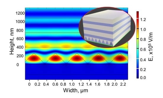
It can be readily observed that incident light couples to the SPP on the conductive surface via a diffractive grating at 940 nm (
Figure 4). Expectedly, this mode does not exist, neither for TE polarization nor for a photonic crystal without a diffraction grating (i.e., for the structure shown in
Figure 1a). The coupling between TPP and SPP is observable for both TM and TE polarizations at 1040 nm and 1060 nm (
Figure 5 and
Figure 6). An exponential decrease in field intensity with distance from the conductive layer characteristic for the optical Tamm state is also readily seen. There is a significant blue shift of optical Tamm state’s wavelength due to diffractive modes providing additional phase matching. Furthermore, resonant dips are also much narrower due to reduced losses of the conductive material associated with the blue shift, a feat usually achieved by adding dielectric layers to the photonic crystal.
Full dispersion for both TM and TE polarization for our simple structure (
Figure 1a) utilizing MXenes is shown in
Figure 7 where the reflection dip due to OTS is easily observed. What can also be seen is the existence of SPPs for TM polarization at large incidence angles and at longer wavelengths.
Full dispersions for TM and TE polarizations for our structure with a diffraction grating (
Figure 1b) are shown in
Figure 8 and
Figure 9. The presence of a diffractive grating acting as a coupler allows for notable coupling and hybridization of TPP and plasmonic modes of the structure for TM polarization (
Figure 8 top), significantly broadening the transparent band and improving the coupling strength, resulting in even lower reflection. Since scatterers can convert between propagating and evanescent when the structure is illuminated from the other side for extremely large incident angles, it allows for evanescent modes, due to the total reflection leaking out due to radiative scattering (
Figure 8 bottom).
For TE polarization, we have an exactly opposite situation since there are no SPP modes for this polarization and the transparent band due to OTS breaks for SPP modes (
Figure 9 top). Since the diffraction grating has no change in the refractive index in the direction of the electric field, there is also no leakage when the structure is illuminated from the other side (
Figure 9 bottom), allowing MXenes to practically omnidirectionally screen the entire structure.
As far as the influence of the grating size variations on the electromagnetic response is concerned, any increase in the grating constant will cause a corresponding redshift of the spectral dispersion. This is in line with the scalability of Maxwell equations, a fact that is universally used in plasmonic dispersion tailoring. Conversely, a shortening of the base would be followed by a blueshift. For plasmonic materials, redshift means larger material losses, while the reverse is true for blueshift). However, the spectral dispersion shifting relation with the grating constant is just one detail of the consideration, and the main points remain the material, directional, polarization, and angular dependencies. While general qualitative trends are already clear, a full quantitative exploration of the effects of the grating constant variations in correlation with all the other parameters would require extensive additional calculations. Such a feat would vastly surpass the aims and purposes of the present manuscript.


