Abstract
In the present work, Mo/VC multilayers with constant period (10 nm) and different modulation ratios (from 6:4 to 9:1) were deposited by dc magnetron sputtering. We investigated the microstructure and mechanical properties of Mo/VC multilayers. XRD and TEM results indicated that Mo was a bcc structure and VC was a NaCl B1 (fcc) structure. An HRTEM image revealed the coherent interfaces between the Mo and VC layers. Hardness and toughness were studied using the Nanoindent and Microindent methods, respectively. It was found that the multilayers hardness remained as high as ~22 GPa, while the toughness increased from 2.91 to 4.70 MPa·m1/2 and the modulation ratio varied from 6:4 to 9:1. The enhancement of both hardness and toughness is attributed to the interfaces and the lamellated structure. The first-principles method was also used to determine the most stable interface model and the formation mechanism of the interface between the Mo and VC layers.
1. Introduction
The toughening of hard coatings has drawn increasing research attention the recent decades. However, the antagonism between hardness and toughness makes it a great challenge to realize the synchronous optimization of such coatings [1,2,3,4]. A number of studies have shown that the nacre layer of the shell adopts hard hydroxyapatite and soft collagen to achieve a toughness that is 3000 times higher than its components, in addition to maintaining a high strength through the multilayer structure [5,6]. This suggests that the soft-hard architectural structure can be considered for toughening hard coatings [7,8,9,10]. Metal-ceramic multilayers seem to be the desired design for the preparation of hard and tough coatings. It was reported that enhanced plastic co-deformation was performed in Al/TiN nanolayered coatings, which provided the possibility of high hardness and improved ductility for nanoscale metal-ceramic multilayers [11]. Yuan et al. [12] synthesized the Ti/TiN multilayer coating and showed that the coating had the maximum hardness and Young’s modulus, while retaining good fracture toughness and crack resistance. Shi et al. [13] found that the hardness of W/VC multilayer coatings with a 10 nm bilayer period were measured to be 28~30 GPa, which were harder than pure VC. The toughness of the coatings increased from 3 to 7.5 MPa·m1/2 with the W fraction from 60% to 90%. All of the coatings exhibited significant hardness and toughness enhancement. In addition to the layer structure, the interfacial characteristic is another key factor with regard to the toughening of hard coatings [14], which is a benefit for the confinement of dislocation gliding, such as dislocation pile-up near the interface and a single dislocation bowing in layers [15]. When the layer thickness is small enough, dislocations slip across the interface [16] and can facilitate energy dissipation. Thus, complex interfaces, avoiding stress concentration, can redistribute the stress at the crack tip over a larger area.
As a hard high-melting point metal, Mo is considered to be one of the best wear resistant coating materials [17]. While VC can reach a hardness of 25 GPa and has a low coefficient of friction [18], especially at high temperatures when V2O5 generates [19], it can be used as a solid lubricant in high-speed cutting. Therefore, Mo/VC multilayers, in which the metal phase offered the toughness and ceramic phase provided the hardness, are proposed as a great potentially protective coating in this paper. The relationship between the hardness and toughness of these multilayers was explored. Moreover, we also focused on the interface structure to explore the interface toughening mechanism.
2. Materials and Methods
2.1. Synthesis
Four different Mo/VC multilayers, of which the modulation ratio ƞMo/VC = lMo:lVC (lMo represents the Mo layer thickness, lVC represents the VC layer thickness) which varied from 6:4 to 9:1 with the fixed modulation period Λ(lMo + lVC) = 10 nm, were deposited onto polished silicon (100) substrates using dual-cathode DC magnetron sputtering in an argon (99.99%) environment at ambient temperature. For all multilayers, the deposition started with the growth of a 30 nm VC buffer layer followed by 57 bilayers of Mo and VC for a total thickness of 600 nm. The buffer VC layer was deposited to prevent the reaction between the Si substrate and Mo. The power for two targets of Mo (Φ50 × δ3 mm) and VC (Φ50 × δ3 mm) were 100 and 200 W, respectively. The substrate-to-target distance is 100 mm. The substrate was biased at −100 V during deposition to improve film densification by ion bombardment of the growing film. The base pressure in the chamber was less than 1 × 10⁻⁵ Pa, and the working pressure was set at 0.5 Pa. The deposition rate for Mo was 11.3 nm/min, while that for VC was 6.7 nm/min. The modulation ratio ƞMo/VC was achieved through computer control of the shutters in front of the Mo and VC targets. The opening time of the shutters was calculated from the deposition rate, as shown in Table 1. Prior to deposition, all silicon (100) substrates were cleaned in an ultrasonic bath of acetone and methanol sequentially for 30 min, and then ion cleaned at –500 V bias in a 6.5 Pa argon plasma pressure for 15 min to remove surface contaminants.

Table 1.
The opening time of the Mo and VC shutters.
2.2. Characterization
The crystalline structure of the coatings was determined by grazing incidence X-ray diffraction (GIXRD) using the Cu Kα line. The multilayer structure, bilayer periods and interface details were confirmed by transmission electron microscopy (TEM). Nanoindentation tests were conducted using the Hysitron nanoindentor with a Berkovich diamond tip. The hardness (H) and elastic modulus (E) of the coatings were measured by the continuous stiffness measurement (CSM) method. The micro-indentation method as described by Xia et al. [20] was used to determine coating toughness. In this method, the coating is deposited on the Si substrate through a mask to create a sharp edge. A Vickers indentation was performed near the edge on the uncoated Si substrate. Figure 1 shows the indentation geometry. The coating toughness KC is calculated by the following equation:
where KS is Si substrate toughness, a and b are the lengths of indentation cracks growing into and away from the coating, respectively, ϕ is the slope of a versus b, t is coating thickness, σr is residual stress, is the effective elastic modulus given by Ec,s/(1 − ), and subscript c and s describe the coating and substrate, respectively, and ν is the Poisson ratio. The + and − signs are for tensile and compressive residual stresses, respectively.
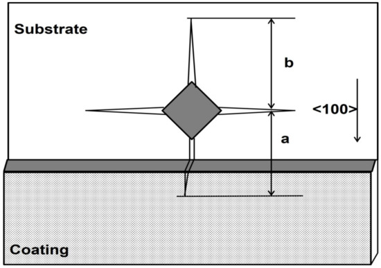
Figure 1.
Schematic of the indentation geometry [20].
A standard Vickers indentation was performed to obtain the indents. Here, 0.5, 1 and 2 N loads were used to make sure the crack propagates into the coating with no delamination, and 20 available indentations were obtained for each load. The associated crack patterns were observed using a scanning electron microscope (SEM). The residual stress was calculated from the Stoney equation via measurements of the wafer curvature by stylus profilometry before and after deposition. It should be emphasized that three replicates for the coatings toughness test were performed in order to establish the accuracy of the results.
2.3. First-Principles Calculations
The interface theoretical calculations presented in this paper were carried out using the Cambridge serial total energy package (CASTEP) code in the framework of the first-principles pseudo-potential method. The generalized gradient approximation (GGA) of Perdew, Burke and Ernzerhof (PBE) [21] was employed as an exchange-correlation function to optimize the geometry of the unit cells of bulk Mo and VC. The K-points were set as 11 × 11 × 9 and 11 × 11 × 11 for Mo and VC unit cells, respectively, as the plane wave cutoff energy of 550 eV was used in all calculations. The calculated lattice parameters for Mo (0.31469 nm) and VC (0.41675 nm) are comparable with the available experimental values [22,23].
A Mo(110)/VC(111) interface was constructed by a supercell approach with periodic boundary conditions, and a vacuum layer with 10 Å was employed to eliminate the periodic interaction between the free surfaces of Mo and VC along the z-axis. K-points were set as 11 × 11 × 1 for the Mo(110)/VC(111) interface. The SCF convergence threshold was set to be 5.0 × 10⁻⁷ eV/atom to obtain the ground state by solving the Kohn-Sham equation [24]. The atoms were relaxed to achieve the minimum total energy of the system to fulfill the geometry optimization by using the Broyden-Fletcher-Goldfard-Shanno (BFGS) algorithm, while the convergence tolerances were 5.0 × 10⁻⁶ eV/atom for energy and 0.01 eV/Å for the maximum force [25].
3. Results and Discussion
3.1. Microstructure
Figure 2 shows the grazing incidence X-ray diffraction (GIXRD) spectra for Mo/VC multilayers with various modulation ratios ƞMo/VC from 6:4 to 9:1. The results indicate that the multilayers are polycrystalline. All peaks of Mo(110), (200) and (211), which are preferred to the bcc structure [26], are expected to be sharper in this 2θ range as the Mo concentration increases. In addition, the B1 NaCl type peaks of VC(111), (200) and (220) [27] are identified at 2θ = 38.1°, 43.4°and 62.8° for multilayers with ƞMo/VC = 6:4 and 7:3. As ƞMo/VC changes to 8:2 and 9:1, the VC peaks are broadening and virtually indistinguishable from the background due to the lower concentration and smaller layer thickness of the VC [13].
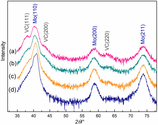
Figure 2.
GIXRD spectra of Mo/VC multilayers: (a) ηMo/VC = 6:4, (b) ηMo/VC = 7:3, (c) ηMo/VC = 8:2, (d) ηMo/VC = 9:1.
The bright-field cross-sectional TEM micrograph of Mo/VC multilayers with modulation ratios ηMo/VC = 8:2 is displayed in Figure 3a. The multilayers, showing a dense columnar structure, disclosed alternating bright (VC) and dark (Mo) layers in a growth direction. The average thickness of the Mo layer is 7.8 nm, while that of the VC layer is 2.2 nm, consistent with the controlled value. The corresponding electron diffraction pattern of the cross-section sample is shown in Figure 3b. Mo and VC reflections are clearly visible, which matches the typical bcc and fcc (B1) polycrystalline structures, respectively. The lattice spacing of Mo was 0.315 nm and the VC was 0.418 nm, supporting the GIXRD results.
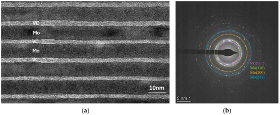
Figure 3.
Cross-sectional TEM images of Mo/VC multilayers with ηMo/VC = 8:2: (a) Bright field image, (b) Corresponding diffraction pattern.
3.2. Mechanical Properties
3.2.1. Hardness and Modulus
Figure 4a,b depict the variation in hardness (H) and elastic modulus (E) as a function of displacement for Mo/VC multilayers with different modulation ratios, respectively. One can see that plateaus occur for the hardness curves in the displacement range from 60–90 nm, which is a 10%–15% coating thickness (600 nm), and is assumed to be the coating hardness with negligible substrate effects, as well as the modulus curves. When the displacement goes beyond 90 nm, the hardness and modulus begin to reduce due to substrate effects.
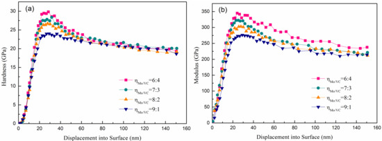
Figure 4.
(a) Hardness and (b) Modulus of Mo/VC multilayers as a function of displacement onto the surface.
For the Mo/VC multilayers with modulation ratio from 6:4 to 9:1, as Figure 5 shown, the hardness values were measured to be 22.93, 22.57, 22.47 and 22.02 GPa, While the elastic modulus values were measured to be 261, 254, 249, and 239 GPa.
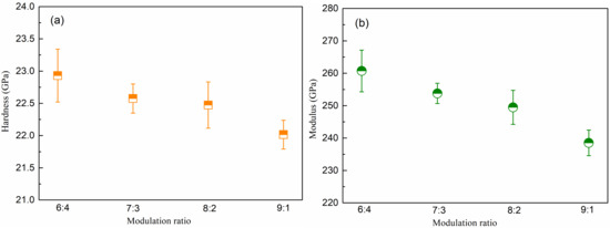
Figure 5.
(a) Hardness and (b) Modulus of Mo/VC multilayers with varied modulation ratios from 6:4 to 9:1.
3.2.2. Toughness
Figure 6 shows the toughness of Mo/VC multilayers determined by the microindentation method. It was noted that as toughness for Mo/VC multilayers increased by 62% from 2.91 to 4.70 MPa·m1/2 with modulation ratios varying from 6:4 to 9:1, the hardness (in Figure 5) is almost sustained, with only 6% reduced. The trade-off between hardness and toughness was apparent, although the mechanical properties of Mo/VC multilayers have not reached the high level of biomaterial properties. This result is due to a combination of several factors, such as the nano-scale grain size [28], the different modulus between the two neighboring layers [29], and interfaces [30,31,32,33,34,35]. Particularly, coherent interfaces not only improve the hardness of the multilayers by alternating the stress field acting as obstacles slipping, but also enhance the toughness by coherency stress activating the dislocation motion near the interfaces. In general, heterogeneous fcc/bcc coherent interfaces produce higher drag force to block the threading dislocation migration compared with a coherent interface with same crystal structure [36]. It is possible for coherent interfaces to absorb or accommodate dislocations due to stress induction, which also mediates dislocations across the interfaces, thus the multilayer toughness improves [30]. Figure 7 shows the indentation with crack pattern, while Table 2 lists the parameters required for toughness calculation.
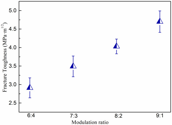
Figure 6.
Toughness of Mo/VC multilayers with varied modulation ratios from 6:4 to 9:1.
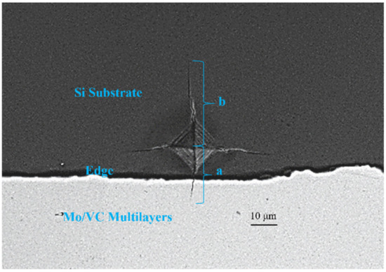
Figure 7.
Image of indentation with crack pattern for Mo/VC multilayers with ƞMo/VC = 8:2.
Table 2.
Parameters required for toughness of Mo/VC multilayers.
3.3. Interface Details
3.3.1. Interfacial Structure
One can believe that interfaces play an important role for the mechanical properties as discussed in the preceding paragraphs of this paper. Thus, a high-resolution TEM analysis was carried out to reveal the interfacial structure, as Figure 8 presents. Interfaces between the multilayers exhibit a strong Kurdjumov–Sachs (K–S) orientation relationship in the growth direction: Mo{110}//VC{111}, Mo < 111 >//VC < 110 >. This means that coherent interfaces were formed between Mo and VC. The corresponding regions revealed the coherent interfaces across the layers, asshown in Figure 6b–e.
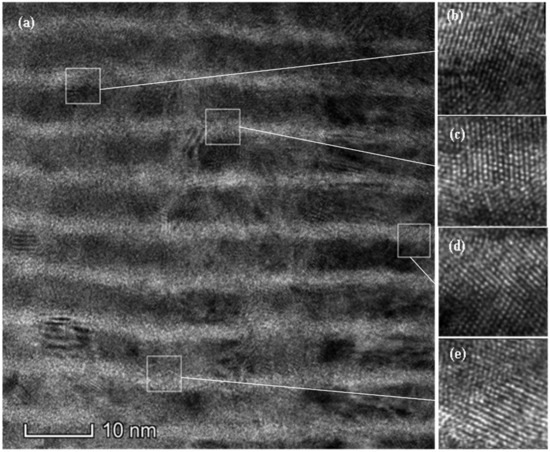
Figure 8.
(a) High-resolution TEM image of Mo/VC multilayers with ƞMo/VC = 8:2, (b–e) Coherent interfaces details.
The Mo/VC interface structure with an Mo{110}//VC{111} orientation relationship was also simulated by a first-principles calculation. As shown in Figure 9, considering two terminations of VC(111) (V- and C-termination) and a three stacking sequence (top-, center- and hollow-site), six different Mo(110)/VC(111) interface geometries were built, where top-, center-, and hollow-site means that the Mo is on the top of the surface atoms, the second layer atoms, and the third layer atoms of the VC layer, respectively.
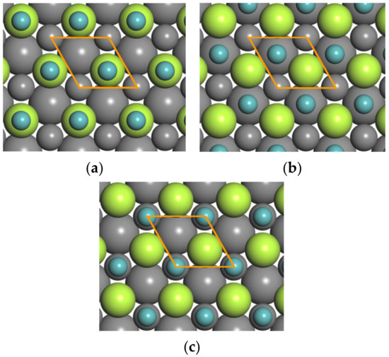
Figure 9.
Interface geometries for C-terminated Mo(110)/VC(111) with three stacking sites: (a) top, (b) center, (c) hollow (The gray ball represents the V atom, the green ball represents the C atom, and the blue ball represents the Mo atom.).
3.3.2. Work of Adhesion
The work of adhesion Wad is an important thermodynamic quantity to characterize the interfacial bonding of the interface. It can be calculated as follows [37]:
where Elayer,Mo and Elayer,VC are the total energies of the fully relaxed surface layers, EMo/VC is the total energy of the interface model, and A is the area of the interface. Table 3 summarizes the result of d0 and calculated Wad for different interface geometries. Table 4 lists the relevant data required for Wad calculation. The Wad value of C-terminated top-, center- and hollow-site interfacial geometry, which increases with optimal interfacial separation reduction, are 5.66, 9.22 and 10.64 J·m−2, respectively. The Wad value of V-terminated top-site, center-site and hollow-site interfacial geometry are 3.77, 5.43 and 5.76 J·m−2, respectively, which are smaller than those of the C-terminated interfaces. This may be because the interface between the Mo layer and the C-terminated VC layer generates more polar covalent bonds, which appear to be stronger than metallic bonds. In particular, the C-terminated hollow-site interface has the highest value of Wad (10.64 J·m−2) among all the considered interface geometries. Meanwhile, the d0 values of the C-terminated interfacial geometries are less than that of the V-terminated interfacial geometries. It can be seen that the termination of VC(111) plays a vital role in the interfacial bonding of the Mo(110)/VC(111) interface compared to the stacking sequence, and the Mo-C bonding at the interface is presumably formed during the fabrication of Mo/VC multilayers.
Wad = (Elayer,Mo + Elayer,VC − EMo/VC)/A
Table 3.
Interfacial separation (d0) and calculated work of adhesion (Wad) of different interfacial geometries after full relaxation.
Table 4.
Relevant data required for Wad calculation.
3.3.3. Density of States
Because the C-terminated hollow-site interface has the strongest adhesion, the partial density of states (PDOS) has been calculated to further comprehend the bonding nature of the Mo(110)/VC(111) interface. The plots are displayed in Figure 10. The PDOS curves of the interfacial layers are significantly different from the interior layers. The interfacial Mo layer in Mo(110) shows new peaks around −5, −6.5, and −11.7 eV, which are resonant with the peaks of the interfacial C layer and the second V layer in VC(111). These resonant peaks are caused by the hybridization between the interfacial C-s orbits, C-p orbits and Mo-d orbits. Moreover, the height of the PDOS curve for the interfacial Mo layer is lower than that of the interior atoms. This indicates the strong Mo-C interfacial interaction and the formation of the strong Mo-C covalent bonds.
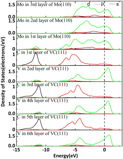
Figure 10.
PDOS of C-terminated hollow-site interface (The vertical dash line indicates the Fermi level).
4. Conclusions
A set of Mo/VC multilayers was deposited onto Si(100) substrates using dual-cathode dc magnetron sputtering. The XRD and TEM results indicated that the multilayers were polycrystalline, as Mo was a bcc structure and VC was a NaCl B1(fcc) structure. The coherent interface along the Mo{110}//VC{111} orientation was also observed. With modulation ratios of Mo/VC multilayers varying from 6:4 to 9:1, hardness was almost sustained, with only a 6% decrease, while toughness increased by 62% from 2.91 to 4.70 MPa·m1/2 The trade-off between hardness and toughness was determined. We attribute this enhancement to the coherent interfaces. The first-principles calculation result indicated that the C-terminated hollow-site interface was the most possible stacking position for the atoms near the interface. The Wad value and PDOS results implied that a strong bonding was produced between the Mo and VC.
Author Contributions
Conceptualization, C.W.; methodology, N.J. and L.T.; writing—original draft, W.X. and H.L.; writing—review and editing, W.X. and C.W.; supervision, X.L.; project administration, C.W.; funding acquisition, Y.L. and W.L. All authors have read and agreed to the published version of the manuscript.
Funding
This work is supported by the National Natural Science Foundation of China (NSFC) (Contract Nos. 51902254, 52004295 and 51902252) and the Natural Science Foundation of Shaanxi Province (Nos. 2018JM5108, 2022JM-261 and 2022JQ-371).
Institutional Review Board Statement
Not applicable.
Informed Consent Statement
Not applicable.
Data Availability Statement
Data sharing is not applicable to this article.
Conflicts of Interest
The authors declare no conflict of interest.
References
- Zhang, S.; Wang, H.L.; Ong, S.E.; Sun, D.; Bui, X.L. Hard yet tough nanocomposite coatings—Present status and future trends. Plasma Process. Polym. 2007, 4, 219–228. [Google Scholar] [CrossRef]
- Wang, X.Y.; Zhang, S.; Lee, J.W.; Lew, S.W.; Sun, D.; Li, B. Hard Yet tough ceramic coating: Not a dream any more—I. via nanostructured multilayering. Nanosci. Nanotech. Let. 2012, 4, 375–377. [Google Scholar] [CrossRef]
- Bhattacharyya, A.S.; Kumar, R.P.; Priyadarshi, S.; Shivam, S.; Anshu, S. Nanoindentation stress–strain for fracture analysis and computational modeling for hardness and modulus. J. Mater. Eng. Perform. 2018, 27, 2719–2726. [Google Scholar] [CrossRef]
- Kindlund, H.; Sangiovanni, D.G.; Martínez-de-Olcoz, L.; Lu, J.; Jensen, J.; Birch, J.; Petrov, I.; Greene, J.E.; Chirita, V.; Hultman, L. Toughness enhancement in hard ceramic thin films by alloy design. APL Mater. 2013, 1, 042104. [Google Scholar] [CrossRef]
- Podsiadlo, P.; Kaushik, A.K.; Arruda, E.M.; Waas, A.M.; Shim, B.S.; Xu, J.; Nandivada, H.; Pumplin, B.G.; Lahann, J.; Ramamoorthy, A.; et al. Ultrastrong and stiff layered polymer nanocomposites. Science 2007, 318, 80–83. [Google Scholar] [CrossRef]
- Tang, Z.; Wang, Y.; Podsiadlo, P.; Kotov, N. Biomedical applications of layer-by-layer assembly: From biomimetics to tissue engineering. Adv. Mater. 2007, 19, 3203–3224. [Google Scholar] [CrossRef]
- Munch, E.; Launey, M.E.; Alsem, D.H.; Saiz, E.; Tomsia, A.P.; Ritchie, R.O. Tough, Bio-inspired hybrid materials. Science 2008, 322, 1516–1520. [Google Scholar] [CrossRef]
- Zhang, Y.; Heim, F.M.; Bartlett, J.L.; Song, N.; Isheim, D.; Li, X. Bioinspired, graphene-enabled Ni composites with high strength and toughness. Sci. Adv. 2019, 5, eaav5577. [Google Scholar] [CrossRef]
- Poloni, E.; Bouville, F.; Dreimol, C.H.; Niebel, T.P.; Weber, T.; Biedermann, A.R.; Hirt, A.M.; Studart, A.R. Tough metal-ceramic composites with multifunctional nacre-like architecture. Sci. Rep. 2021, 11, 1621. [Google Scholar] [CrossRef]
- Meindlhumer, M.; Zalesak, J.; Pitonak, R.; Todt, J.; Sartory, B.; Burghammer, M.; Stark, A.; Schell, N.; Danile, R.; Keckes, J.F.; et al. Biomimetic hard and tough nanoceramic Ti-Al-N film with self-assembled six-level hierarchy. Nanoscale 2019, 11, 7986–7995. [Google Scholar] [CrossRef]
- Bhattacharyya, D.; Mara, N.A.; Dickerson, P.; Hoagland, R.G.; Misra, A. Compressive flow behavior of Al–TiN multilayers at nanometer scale layer thickness. Acta Mater. 2011, 59, 3804–3816. [Google Scholar] [CrossRef]
- Santaella-González, J.B.; Hernández-Torres, J.; Morales-Hernández, J.; Flores-Ramírez, N.; Ferreira-Palma, C.; Rodríguez-Jiménez, R.C.; García-González, L. Effect of the number of bilayers in Ti/TiN coatings on AISI 316L deposited by sputtering on their hardness, adhesion, and wear. Mater. Lett. 2022, 316, 132037. [Google Scholar] [CrossRef]
- Shi, K.C.; Wang, C.; Gross, C.; Chung, Y.W. Reversing the inverse hardness-toughness trend using W/VC multilayer coatings. Surf. Coat. Technol. 2015, 284, 80–84. [Google Scholar] [CrossRef]
- Mara, N.A.; Beyerlein, I.J. Review: Effect of bimetal interface structure on the mechanical behavior of Cu-Nb fcc-bcc nanolayered composites. J. Mater. Sci. 2014, 49, 6497–6516. [Google Scholar] [CrossRef]
- Abadias, G.; Kanoun, M.B.; Goumri-Said, S.; Koutsokeras, L.; Dub, S.N.; Djemia, P. Electronic structure, and mechanical properties of ternary ZrTaN alloys studied by ab initio calculations and thin-film growth experiments. Phys. Rev. B 2014, 90, 144107. [Google Scholar] [CrossRef]
- Hou, Z.; Zhang, J.; Zhang, P.; Wu, K.; Li, J.; Wang, Y.; Liu, G.; Zhang, G.; Sun, J. Modulation-dependent deformation behavior and strengthening response in nanostructured Ti/Zr multilayers. Appl. Surf. Sci. 2020, 502, 144118. [Google Scholar] [CrossRef]
- Romankov, S.; Hayasaka, Y.; Kasai, E.; Yoon, J.M. Fabrication of nanostructured Mo coatings on Al and Ti substrates by ball impact cladding. Surf. Coat. Technol. 2010, 205, 2313–2321. [Google Scholar] [CrossRef]
- Ferro, D.; Rau, J.V.; Generosi, A.; Albertini, R.A.; Latini, A.; Barinov, S.M. Electron beam deposited VC and NbC thin films on titanium: Hardness and energy-dispersive X-ray diffraction study. Surf. Coat. Technol. 2008, 202, 2162–2168. [Google Scholar] [CrossRef]
- Woydt, M.; Skopp, A.; Dorfel, I.; Witke, K. Wear engineering oxides/anti-wear oxides. Wear 1998, 218, 84–95. [Google Scholar] [CrossRef]
- Xia, Z.; Curtin, W.A.; Sheldon, B.W. A new method to evaluate the fracture toughness of thin films. Acta Mater. 2004, 52, 3507–3517. [Google Scholar] [CrossRef]
- Dudiy, S.V.; Lundqvist, B.I. Wetting of TiC and TiN by metals. Phys. Rev. B 2004, 69, 125421. [Google Scholar] [CrossRef]
- Kurlov, A.S.; Gusev, A.I. Effect of nonstoichiometry on the lattice constant of cubic vanadium carbide VCy. Phys. Solid State 2017, 59, 1520–1525. [Google Scholar] [CrossRef]
- Madan, A.; Wang, Y.Y.; Barnett, S.A. Enhanced mechanical hardness in epitaxial nonisostructural Mo/NbN and W/NbN superlattices. J. Appl. Phys. 1998, 84, 776–785. [Google Scholar] [CrossRef]
- Kohn, W.; Sham, L.J. Self-consistent equations including exchange and correlation effects. Phys. Rev. A 1965, 140, 1133–1138. [Google Scholar] [CrossRef]
- Karch, K.; Pavone, P.; Windl, W.; Strauch, D.; Bechstedt, F. Ab initio calculation of structural, lattice dynamical, and thermal properties of cubic silicon carbide. Int. J. Quantum Chem. 1995, 56, 801–817. [Google Scholar] [CrossRef]
- Vink, T.J.; Somers, M.A.J.; Daams, J.L.C.; Dirks, A.G. Stress, strain, and microstructure of sputter-deposited Mo thin films. J. Appl. Phys. 1991, 70, 4301–4308. [Google Scholar] [CrossRef]
- Dong, R.E.; Ye, F.X.; Xu, Y.H. Synthesis, Microstructure evolution and wear properties of VCp dense ceramic prepared by in situ synthesis. Sci. Adv. Mater. 2019, 11, 526–532. [Google Scholar] [CrossRef]
- Stueber, M.; Holleck, H.; Leiste, H.; Seemann, K.; Ulrich, S.; Ziebert, C. Concepts for the design of advanced nanoscale PVD multilayer protective thin films. J. Alloys Compd. 2009, 483, 321–333. [Google Scholar] [CrossRef]
- Yang, L.; Liu, C.; Wen, M.; Dai, X.; Zhang, Y.; Chen, X.; Zhang, K. Small atoms as reinforced agent for both hardness and toughness of Group-VIB transition metal films. J. Alloys Compd. 2018, 735, 1105–1110. [Google Scholar] [CrossRef]
- Zhou, S.; Kuang, T.; Qiu, Z.; Zeng, D.; Zhou, K. Microstructural origins of high hardness and toughness in cathodic arc evaporated Cr-Al-N coatings. Appl. Surf. Sci. 2019, 493, 1067–1073. [Google Scholar] [CrossRef]
- Li, Y.P.; Zhang, G.P.; Wang, W.; Tan, J.; Zhu, S.J. On interface strengthening ability in metallic multilayers. Scr. Mater. 2007, 57, 117–120. [Google Scholar] [CrossRef]
- Ivanov, M.B.; Vershinina, T.N.; Ivanisenko, V.V. The effect of composition and microstructure on hardness and toughness of Mo2FeB2 based cermets. Mat. Sci. Eng. A 2019, 763, 138117. [Google Scholar] [CrossRef]
- Chu, X.; Barnett, S.A. Model of superlattice yield stress and hardness enhancements. J. Appl. Phys. 1995, 77, 4403–4411. [Google Scholar] [CrossRef]
- Lu, Y.; Sekido, N.; Yoshimi, K.; Yarmolenko, S.N.; Wei, Q. Microstructures and mechanical properties of Mg/Zr nanostructured multilayers with coherent interface. Thin Solid Film. 2020, 712, 138314. [Google Scholar] [CrossRef]
- Barbé, E.; Fu, C.C.; Sauzay, M. Fracture of coherent interfaces between an fcc metal matrix and the Cr23C6 carbide precipitate from first principles. Phys. Rev. Mater. 2018, 2, 023605. [Google Scholar] [CrossRef]
- Shen, Y.; Anderson, P.M. Transmission of a screw dislocation across a coherent, non-slipping interface. J. Mech. Phys. Solids 2006, 55, 956–979. [Google Scholar] [CrossRef]
- Li, J.; Cui, Y.; Chen, Y.; Lv, X.; Luo, X. Theoretical investigation on SiC(111)/Al4C3(0001) interface using density functional theory calculations. Mater. Today Commun. 2019, 21, 100743. [Google Scholar] [CrossRef]


Disclaimer/Publisher’s Note: The statements, opinions and data contained in all publications are solely those of the individual author(s) and contributor(s) and not of MDPI and/or the editor(s). MDPI and/or the editor(s) disclaim responsibility for any injury to people or property resulting from any ideas, methods, instructions or products referred to in the content. |
© 2023 by the authors. Licensee MDPI, Basel, Switzerland. This article is an open access article distributed under the terms and conditions of the Creative Commons Attribution (CC BY) license (https://creativecommons.org/licenses/by/4.0/).