Article

Effect of a Discontinuous Ag Layer on Optical and Electrical Properties of ZnO/Ag/ZnOStructures

1
Central Laboratory of Solar Energy and New Energy Sources, Bulgarian Academy of Sciences, 72 Tzarigradsko Chaussee Blvd, 1784 Sofia, Bulgaria
2
Institute of Solid State Physics, Bulgarian Academy of Sciences, 72 Tzarigradsko Chaussee Blvd, 1784 Sofia, Bulgaria
3
Physical Sciences, Munster Technological University, Rosa Avenue, Bishopstown, Cork, Ireland and Tyndall National Institute, Lee Maltings, Cork, T12 R5CP, Ireland
4
Institute of Ion Beam Physics and Materials Research, Helmholtz-Zentrum Dresden-Rossendorf (HZDR), BautznerLandstrasse 400, 01328 Dresden, Germany
5
Institute of Electronics, Bulgarian Academy of Sciences, 72 Tsarigradsko Chaussee, 1784 Sofia, Bulgaria
6
School of Engineering, The University of Glasgow, Glasgow G12 0QQ, Scotland, UK
*
Author to whom correspondence should be addressed.
Coatings 2022, 12(9), 1324; https://doi.org/10.3390/coatings12091324
Submission received: 9 August 2022 / Revised: 8 September 2022 / Accepted: 8 September 2022 / Published: 11 September 2022
(This article belongs to the Special Issue Advances of Nanoparticles and Thin Films)

Abstract

:
ZnO/Ag/ZnO nanolaminate structures were deposited by consecutive RF sputtering at room temperature.The optical transparency, sheet resistance, and figure of merit are determined in relation to the deposition time of Ag and to the film thickness of the ZnO top layer. An improved transmittance has been found in the visible spectral range of the ZnO/Ag/ZnO structure compared to ZnO multilayers without Ag. High transmittance of 98% at 550 nm, sheet resistance of 8 Ω/sq, and figure of merit (FOM) of 111.01 × 10⁻³ Ω−1are achieved for an optimized ZnO/Ag/ZnO nanolaminate structure. It is suggested that the good optical and electrical properties are due to the deposition of the discontinuous Ag layer. The electrical metallic type conductivity is caused by planar located silver metal granules. The deposition of a discrete layer of Ag nano-granules is confirmed by atomic force microscopy (AFM) and cross-section high-resolution transmission electron microscopy (HRTEM) observations.

1. Introduction

In solar cells and optoelectronic devices, an ideal transparent top electrode must effectively collect electrical carriers while exhibiting minimal optical and electrical losses. Independent from the application, all transparent electrode materials should combine the following properties: transparency in the spectral range of the device, high lateral conductivity (low sheet resistance), good ohmic contact with adjacent layers, and low impact on the underlying layers during their deposition. Recently, the main objective of developing new materials for transparent conductive oxide (TCO) films is to achieve lower resistivity and higher transmittance in the spectral visible range and to replace the conventional ITO conductors. Transparent conducting oxides (TCOs), namely SnO2, ITO, doped ZnO, etc.,are widely investigated in order to be applied as electrodes in a variety of optoelectronic devices such as solar cells and light-emitting diodes [1]. Among transparent electrodes, metal oxide/metal/metal oxide (OMO) structures can achieve improved optical and electrical performances comparable to single TCO layers and very thin metallic films [2]. The development of ITO-alternative low-cost, earth-abundant, and mechanically stable TCOs exhibiting excellent transparency and electrical properties is very important. OMO structures as multilayer TCOs possess excellent optical and electrical properties that can be achieved at much lower thickness even after combining the individual layer thicknesses [3]. The top and bottom oxide layers provide high optical transparency along with protection for the metal layer from degrading [4]. Thus, a ZnO-based multilayer TCO can be cheaper compared to ITO as the complete thickness of the structure (≤100 nm) is much lower than that of ITO (~400 nm) to obtain similar electrical and optical properties [5].
The optical and electrical properties of oxide/metal/oxide structures are well documented [5,6,7,8,9,10,11,12], demonstrating that the dielectric/metal/dielectric thin films with different metals such as Ag, Au, and Cu have improved conductivity and high optical transmission [5,8,9,10,11,12].
Herein we make use of electrical conductivity in granular (discontinuous) type films [13]. The granules are metallic particles with sizes ranging usually from a few to hundreds of nanometers, embedded into an insulating matrix. The nanolaminate OMO structure is formed using one or two different dielectric layers. The electrical conductivity can be tuned by controlling the lateral dispersion of the metal granules within the nanolaminate. The most important part of the fabrication of nanolaminate OMO structures with specified optical and electrical properties is the deposition of a discontinuous metal layer. The advantages of this approach are reproducibility, effective process control, and a selective formation of conductive areas in a dielectric structure. Nanolaminate structures with dielectric layers such as TiO2, MoOx, and Al2O3 [14], and various metals such as Ag, Cr, Ni, and Pt [15] have been studied. These studies were conducted for various applications of OMO structures [16,17,18] such as indium-free TCO, optoelectronic devices, energy and flexible electronics, and flexible photovoltaic cells.
In this study, we report on the formation of transparent and conductive ZnO/Ag/ZnO nanolaminate structures obtained only by magnetron sputtering at room temperature. Using atomic force microscopy (AFM) and high-resolution transmission electron microscopy (HRTEM) measurements, we evidence that the deposition of Ag on the ZnO layer forms a discontinuous layer. These islands-type structures in conjunction with the optimized thickness of the top zinc oxide layer increase the structure transparency, achieving a high value of the figure of merit: −111 × 10−3 Ω−1. An additional advantage of this structure is that it retains its properties after annealing up to 400°C making it a promising candidate as a highly efficient transparent electrode for optoelectronic devices.

2. Materials and Methods

2.1. Nanolaminate Structure Deposition

ZnO/Ag/ZnO nanolaminate structures were prepared by high-frequency magnetron sputtering technique on glass and Si substrate. The equipment was an RF magnetron sputtering system model CFS-4ES Tokuda system (Tokuda, Seisakusho Co., Ltd., Ginan-cho, Japan)with a 3 sputtering source P-GUN75 (3 inches). The substrate holder was a disk with a diameter of 200 mm and had a water cooling system.The used targets are Ag and ZnO with purities of 99.9% (Kurt J. Lesker; Company LTD., Hastings, UK), respectively. Argon was used as a sputtering gas. The three targets (75 mm in diameter each) were positioned at eccentric positions in front of the substrate holder.The holder was water cooling; therefore a little radiation heat was generated. The targets and the substrate holder were vertically arranged (mode-side sputtering)at a distance of 8 cm. The substrate holder can be rotated at a speed of 10–80 rpm. The three-target configuration allows us to deposit successively different layers without opening the chamber. Sputtering was performed at room temperature without any post-process treatment.The base chamber pressure before the deposition was approximately 1 × 10⁻⁶ mbar and the sputtering process was performed at a chamber pressure of approximately 6 × 10⁻³ mbar for ZnO and 1 × 10⁻³ mbar for Ag. ZnO and Ag were deposited using an RF power of 200 W. During the sputtering process, the substrate holder was rotated at speed of 20 rpm for ZnO and 60 rpm for Ag. The ZnO/Ag/ZnO multilayer structures were consecutively deposited onto glass substrates (Borofloat glass) and Si wafers (p-type CZ, 3″ polished wafers with resistivity 10 Ω.cm). Before being loaded into the sputtering chamber, the glass substrates were cleaned in an ultrasonic bath with deionized water for 15 min and finally dried in a N2 stream.
In our experiments, the deposition times of undercoat and overcoat ZnO layers were 3 min and 6 min, while the deposition time of Ag was set to 5 and 10 s. When Ag is sputtered for a longer time, the metal grains change to high-density distribution. As the result, the conduction ability of fabricated samples is improved. Structures without silver nano-granules were prepared as reference samples under the same conditions. The description of the prepared samples is given in Table 1.
The thickness of ZnO layers was determined by ellipsometric measurements on test samples on a silicon substrate at the different sputtering times of the layers. More complicated is the problem of determining the thickness of the Ag layer. We hypothesize and prove an island structure of Ag granules. In this case with metal islands, where the free space between them is large, the role of the surface substrate dominates.For this reason, we consider that the real thickness cannot be determined from ellipsometric measurements.For this reason, some researchers use the duration of the sputtering process [19] or various Ag deposition rates [20].

2.2. Characterization Methods

The optical properties of the nanolaminate OMO structures are studied by means of UV-VIS-NIR Shimadzu spectrophotometer UV 3300 (Shimadzu Corporation, Kyoto, Japan). Spectral ellipsometry (SE)was applied to optically characterized nanolaminate OMO structures. A spectroscopic ellipsometer J. A. Woollam M-2000 (J.A. Woollam Co. Instruments, Lincoln, NE, USA) was used to acquire film thickness and optical constants in the spectral region of 200–1000 nm. The SE measurements were collected at angles of incidence equal to 45°, 55°, 65°, and 75°, respectively. The sheet resistance was measured using the four-point probe method using a VEECO instrument, model FPP-100, USA.
The surface morphology was investigated by AFM measurements that were carried out using a Multimode V (Bruker, ex. Veeco, Santa Barbara, CA, USA). Imaging was performed in tapping mode and height, with a scan rate of 2 Hz and 512-line image resolution. SEM and HRTEM analyses were performed to evaluate the surface morphology of the Ag layer. TEM analysis was performed with a JEOL 2100, 200 kV (JEOL Ltd., Tokyo, Japan), double tilt holder, beam aligned at the {110} zone axis of the carrier wafer.The cross-section is made with Helios Nanolab Dual Beam FIB (CIC nanoGUNE, San Sebastian, Spain): final thinning at 93 pA 30 kV, final polish 5 kV 56 pA, in situ lift out.

3. Results and Discussions

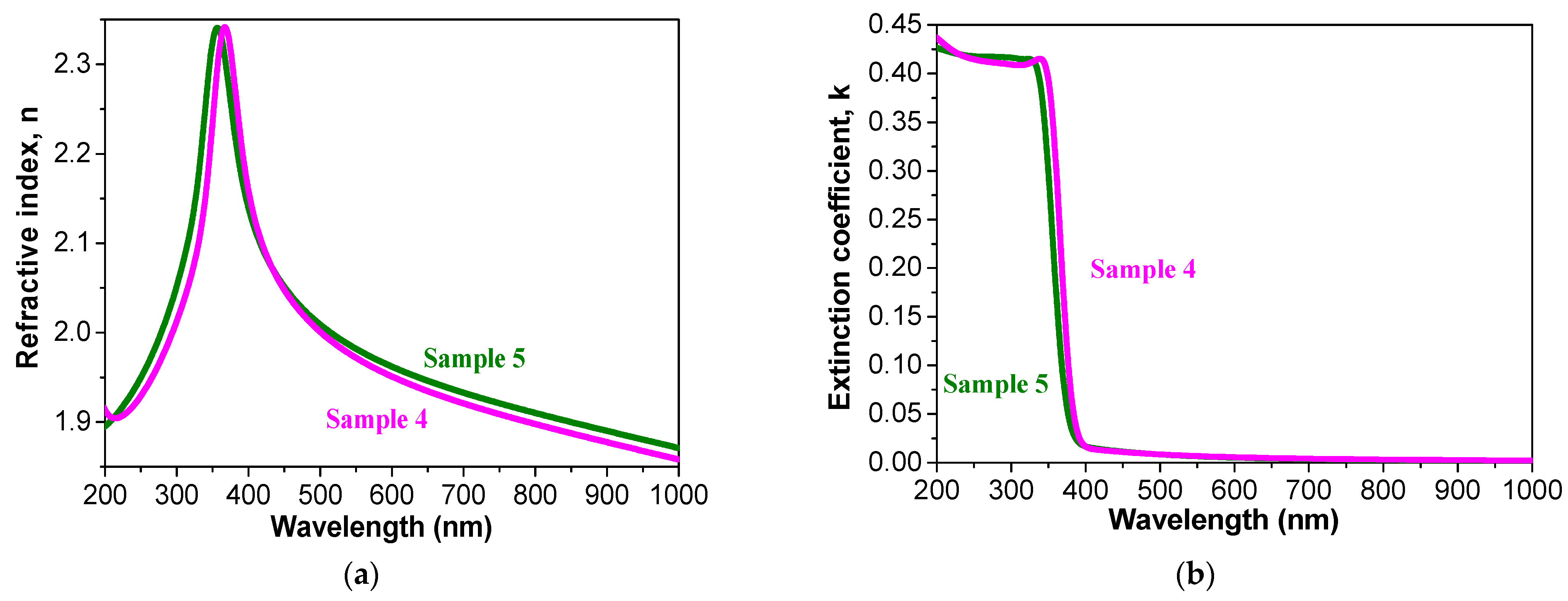
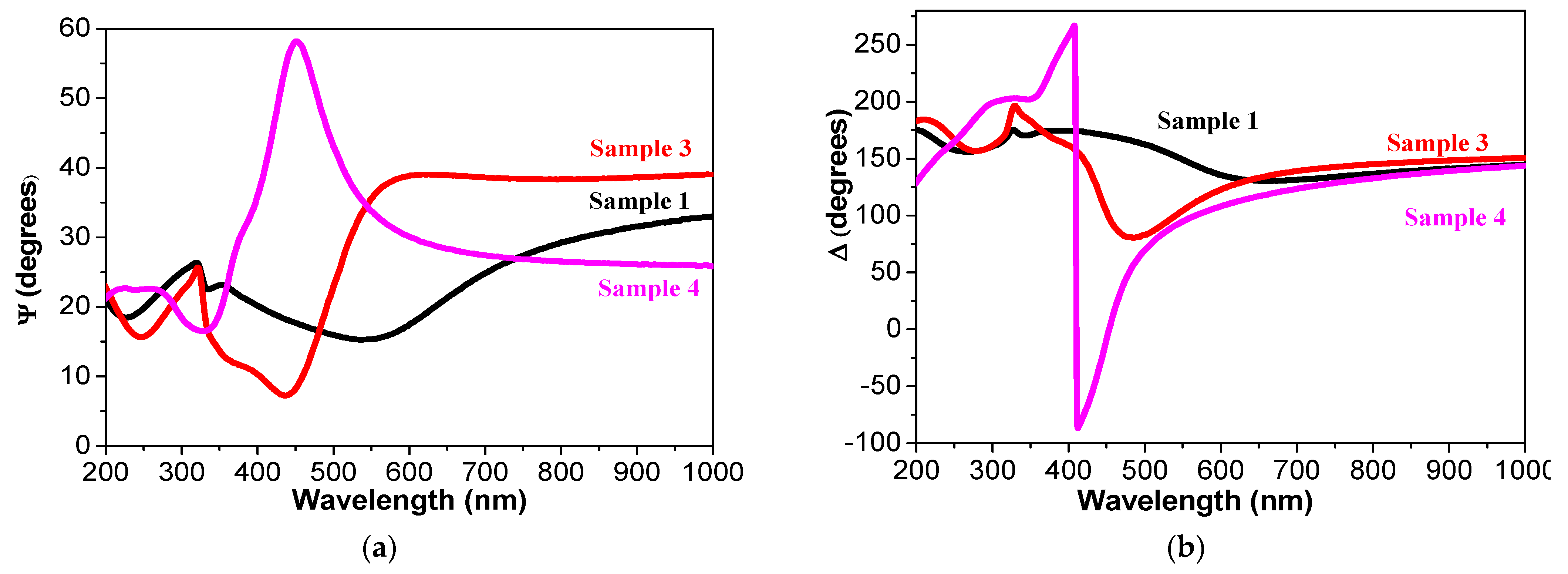
3.1. Ellipsometric Measurements

ZnO structures of different thicknesses deposited on silicon and glass substrates were investigated by applying spectroscopic ellipsometry (SE). SE spectra were measured at room temperature in a spectral range from 193 nm to 1000 nm. The angle of incidence varies between 45° and 75° (10° steps). SE measurements produce two parameters; the amplitude ratio (ψExp) and phase difference (ΔExp) between the incident and the reflected polarized beams. The extraction of the optical constants n and k from the measured quantities ψExp and ΔExp is done using an adequate optical model and fitting procedure. Two types of structures were measured: sample 4 and sample 5 (see Table 1). Sample 4 was obtained after two consecutive ZnO depositions of three minutes each with a pause of 30 s between them. Sample 5, with two ZnO layers, was formed by deposition of the first layer for 3 min and the second one for 6 min.
The refractive index (n) and extinction dispersion (k) of the sputtered ZnO structure are presented in Figure 1. The extinction above 400 nm is very low, indicating the high transparency of the film. The refractive index is varied from 2.04 to 1.86 in the spectral range of 400 to 1000 nm.These values are in agreement with the literature data. The refractive index of sputtered ZnO films is reported to be in the range of 1.96 to 2.06 at 500 nm, depending on the film thickness and technological conditions [21].
The total thickness of the ellipsometric measurements for sample 4 is 58 nm and for sample 5 is 92 nm. The average deposition rate is 9.9 nm/min.
Figure 2 shows the SE parameters ψExp, and ΔExp measured for sample 4 at a different angle of incidence for samples 1, 3, and 4. Samples 1 and 3 are nanolaminate film structures with Ag nano-granules i.e.,ZnO (28 nm)/Ag/ZnO (28 nm), the difference is the density of Ag nano-granules (deposition time of Ag). Sample 4 is only the ZnO layer. These results are similar to the results presented in [22].
The spectral behavior of ψExp and ΔExp depends on the deposition time of silver. This can be used as a technological criterion for the presence of silver particles.

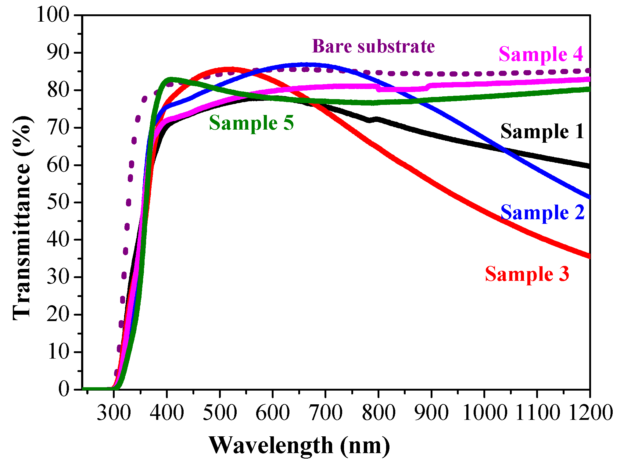
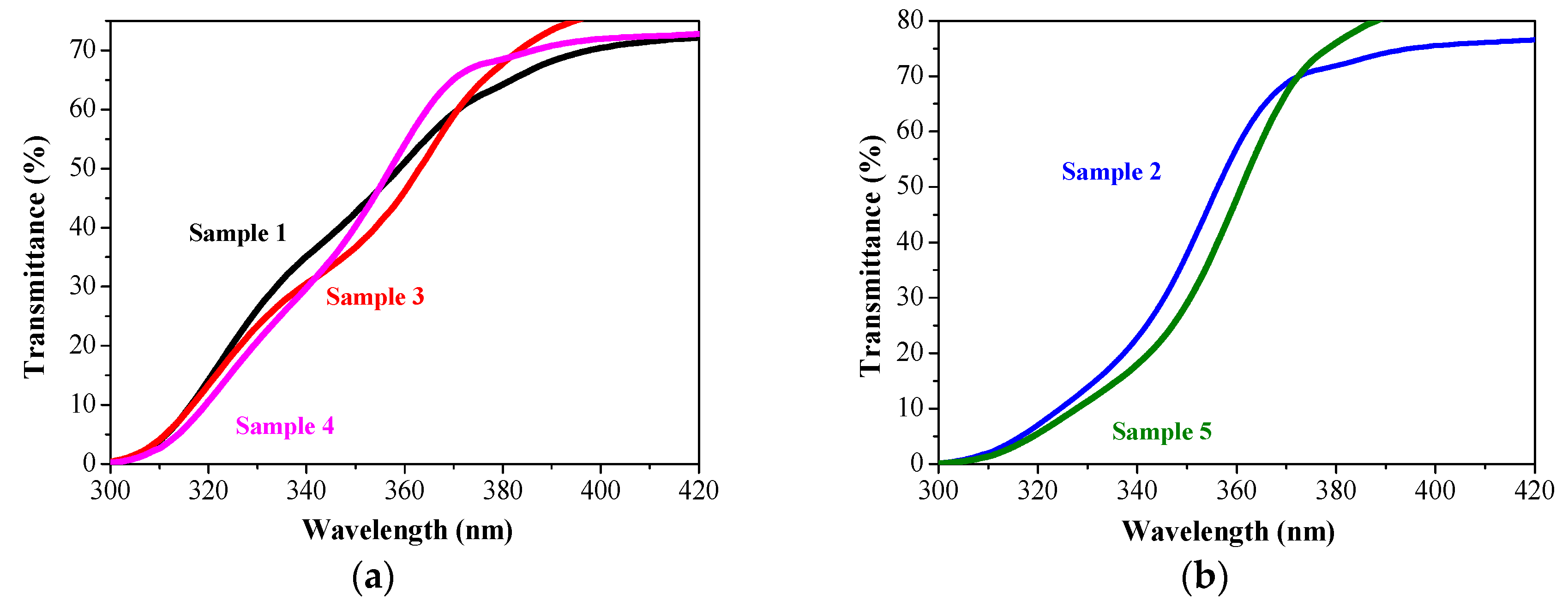
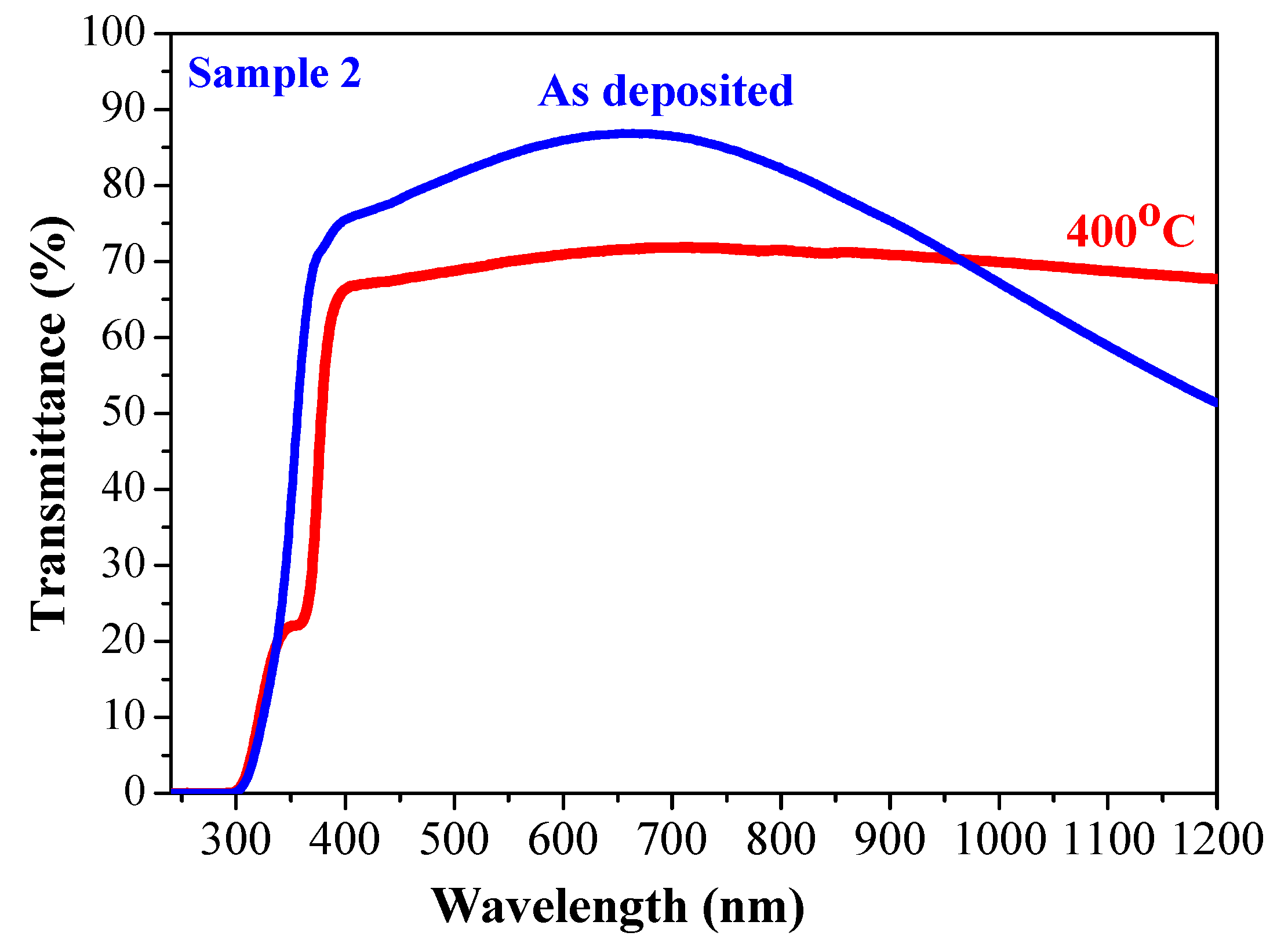
3.2. Optical Properties and Sheet Resistance

Multilayered ZnO/Ag/ZnO structures were deposited layer by layer on glass substrates using an RF magnetron sputtering system. The sputtering time and thickness of the layers are listed in Table 1.
In previous articles [14,15,16], the relationship between optical transmission and sheet resistance of nanolaminate structures of the ZnO/Ag/ZnO type, depending on the thickness of the Ag layer (or deposition time) has been reported. The effect of the thickness of the top layer (ZnO above Ag nano-granules) is also studied in this research. Figure 3 shows the transmittance spectra of the samples described in Table 1.
Table 2 presents the results for the sheet resistance, average transmittance, and figure of merit of the samples from Table 1. In many previous studies of oxide/metal/oxide nanolaminate structures, it has been reported that sheet resistance and optical transmission depend on the thickness of the metal layer [6,8,9]. The thickness of the metal layer varies from 5 nm to 20 nm. Our research shows that increasing the sputtering time increases the density and size of the metal granules, which is the reason for the increase in electrical conductivity. These results are reported for TiO2/Ag/TiO2 nanolaminate structures [15]. A similar dependence for the studied samples ZnO/Ag/ZnO is presented in Table 2 for sample 1 (7 s sputtering time) and sample 3 (10 s). It must be noted that the transmittance is measured against air and the reported transparency values are for the whole system glass substrate + nanolaminate structure. Table 2 presents the average transmittance value in the spectral range of 400–800 nm considering and subtracting the bare glass substrate spectrum. It is seen that the ZnO/Ag/ZnO nanolaminate structures are very transparent reaching almost 98%.
The figure of merit (FOM), proposed by Haacke [23,24], is an effective way to evaluate the electrical and optical properties of transparent conductors and can be determined by:
F O M = T a v 10 R s h e e t ,
where Tav is the average transmittance in the spectral range 400–800 nm and Rsheet is the sheet resistance measured by a four-point probe. The results of FOM are summarized in Table 2.
In Table 3, a comparison of reported sheet resistance and figure of merit of OMO structures, deposited using different methods is given. It must be noted that for commercial ITO, the values are T = 90.2%, Rsheet = 30 Ω/sq, and FOM = 12 × 10−3 Ω−1.The FOM values obtained in this work are close to or even higher than previously reported values (Table 3). Thus, OMO nanolaminate structures with superior optical and electrical properties and figures of merit have been fabricated using consecutive magnetron sputtering at room temperature. The fabricated OMO structures with lower sheet resistance and lower thickness can prove advantageous for reducing the substrate cost in the devices [3,25].
The nanolaminate structures with an equal film thickness as ZnO (sample 1 and sample 3) possess sheet resistance values that decrease when increasing the deposition time of Ag. The comparison between sample 1 and sample 3 reveals that the sheet resistance has been reduced by a factor of two while the silver deposition time was increased from 3 to 6 min. Notably, sample 2, having almost double the thickness of the top ZnO layer in sample 1, showed sheet resistance that is significantly decreased. The effect of the Ag incorporation of the Ag layer and the thicker top layer is also observed in the transmittance spectra (see Figure 4 and Figure 5).
The nanolaminate structure with Ag (sample 2) is more transparent in the visible spectral ranges 450–700 nm when compared to sample 5, with a similar thickness of the ZnO layers but no Ag particle deposition. Similar optical behavior is found for samples 1 and 3 when compared to sample 4 without Ag. Sample 1 has a transparency of 74%–76%, lower than sample 4 (74%–79%). In the near IR region, the transparency of nanolaminate structures with Ag decreases, which is typical of OMO structures. Sample 3 reveals the strongest decrease in the wavelength above 650 nm up to 1200 nm (NIR spectral range), induced most probably by the higher density of the silver particles.
The transmittance spectra of samples 2 and 3 show a broad enhanced transmission in the visible range with maximum transmittances at wavelengths of about 650 nm and 500 nm, respectively. In contrast, the transmittance spectra for sample 1 showed no enhancement of the visible light transmittance. Structurally, sample 1 has received the same sputtering sequence as sample 2, only the thickness of the top ZnO layer has double the thickness (see Figure 3). Such an enhancement of the visible light transmittance by metal (Ag) nano-granule incorporation has already been observed for the ZnO/Ag/ZnO films [37]. The authors of [37] claim that this effect can be attributed to the coupling between the incident light and surface plasmon polaritons (SPPs) of the Ag mid-layer with a layer-plus-islands structure. The coupling or resonance between incident light and SPPs can lead to many interesting physical phenomena, such as extraordinary light transmission [38] and surface-enhanced Raman scattering [39]. In [22], it is also shown that Ag clusters not only have evidently lowest possible absorbance but also might gain from plasmonic features such as re-emission of the light coupled by the SPs at the random silver-island grating or enhanced transmittance.The optical transmission enhancement of ZnO films with incorporated Ag was also investigated by others [40] and they stated that light transmission is enhanced by SPR.
Figure 4 manifests the change of the absorption edge, depending on the Ag layer (different deposition times) and ZnO thickness. The absorption edge is shifted towards the longer wavelengths due to the Ag layer. It is also dependent on the Ag sputtering time. A similar optical behavior of the absorption edge has been previously reported for structures of ZnO/Ag/glass [37,41].
The optical and electrical characterization reveals that Ag granules deposited between two ZnO films lead to improved transparency, lower sheet resistance, and a high figure of merit. These results are encouraging for the application of these nanolaminate structures as highly effective TCOs.

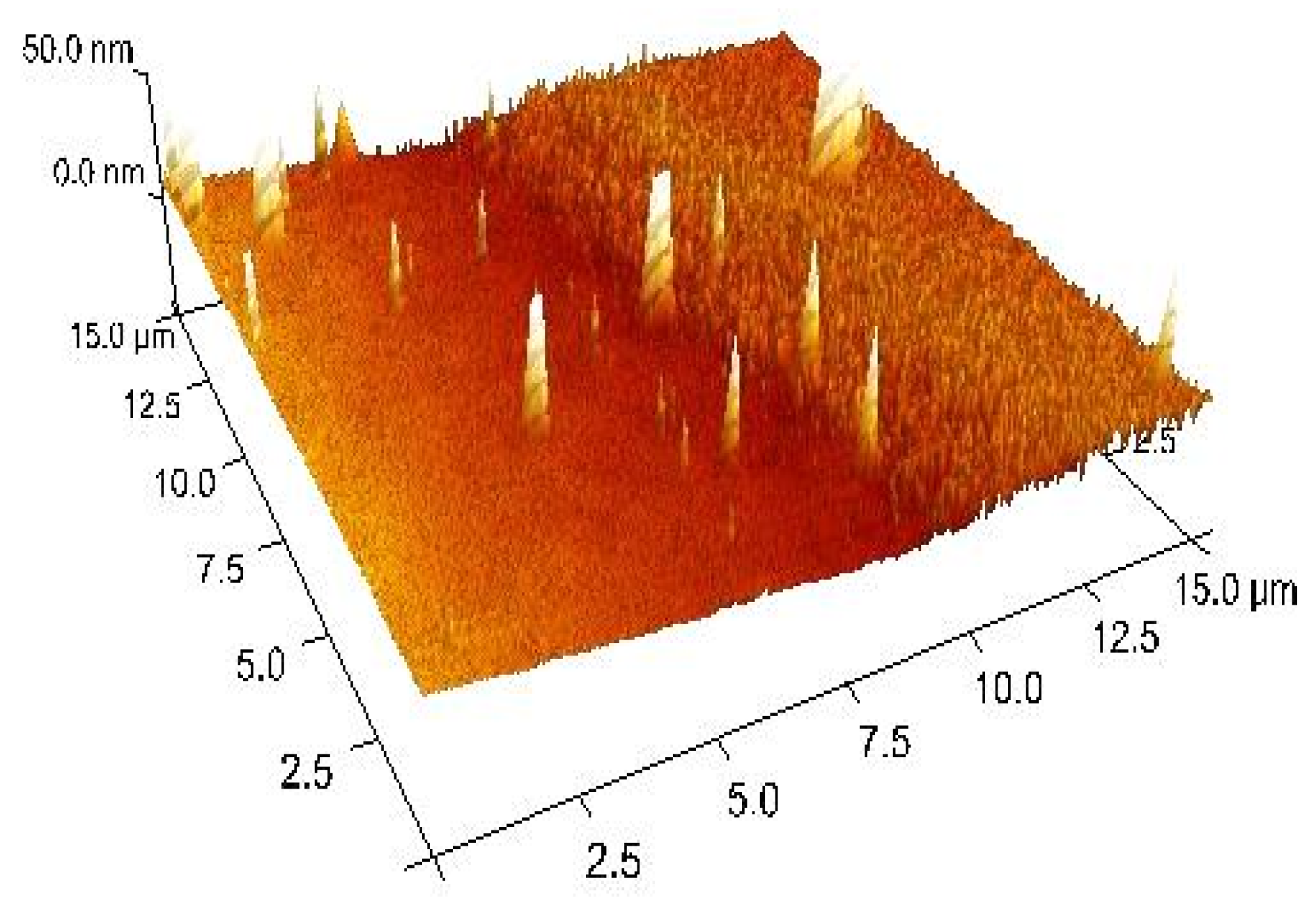
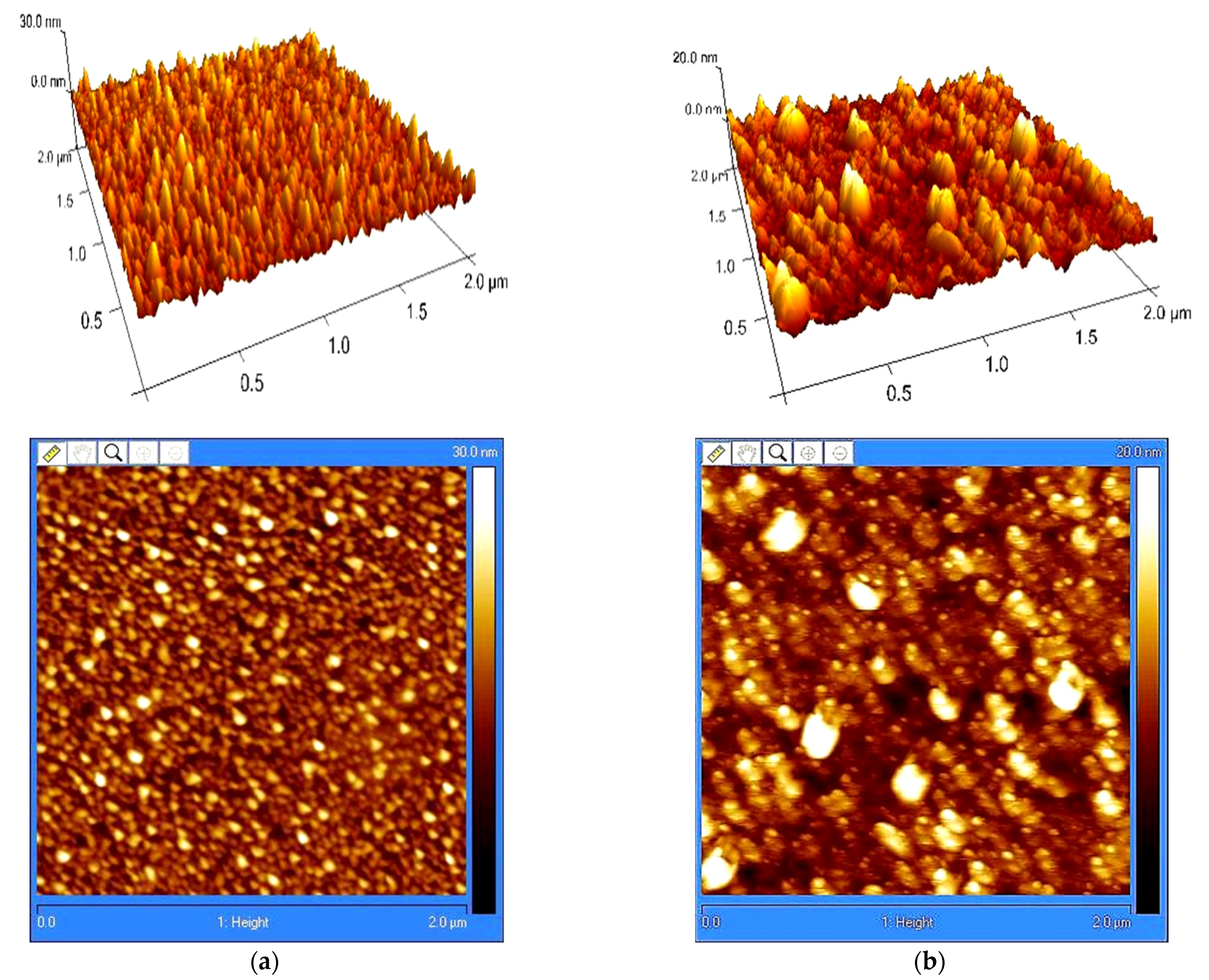
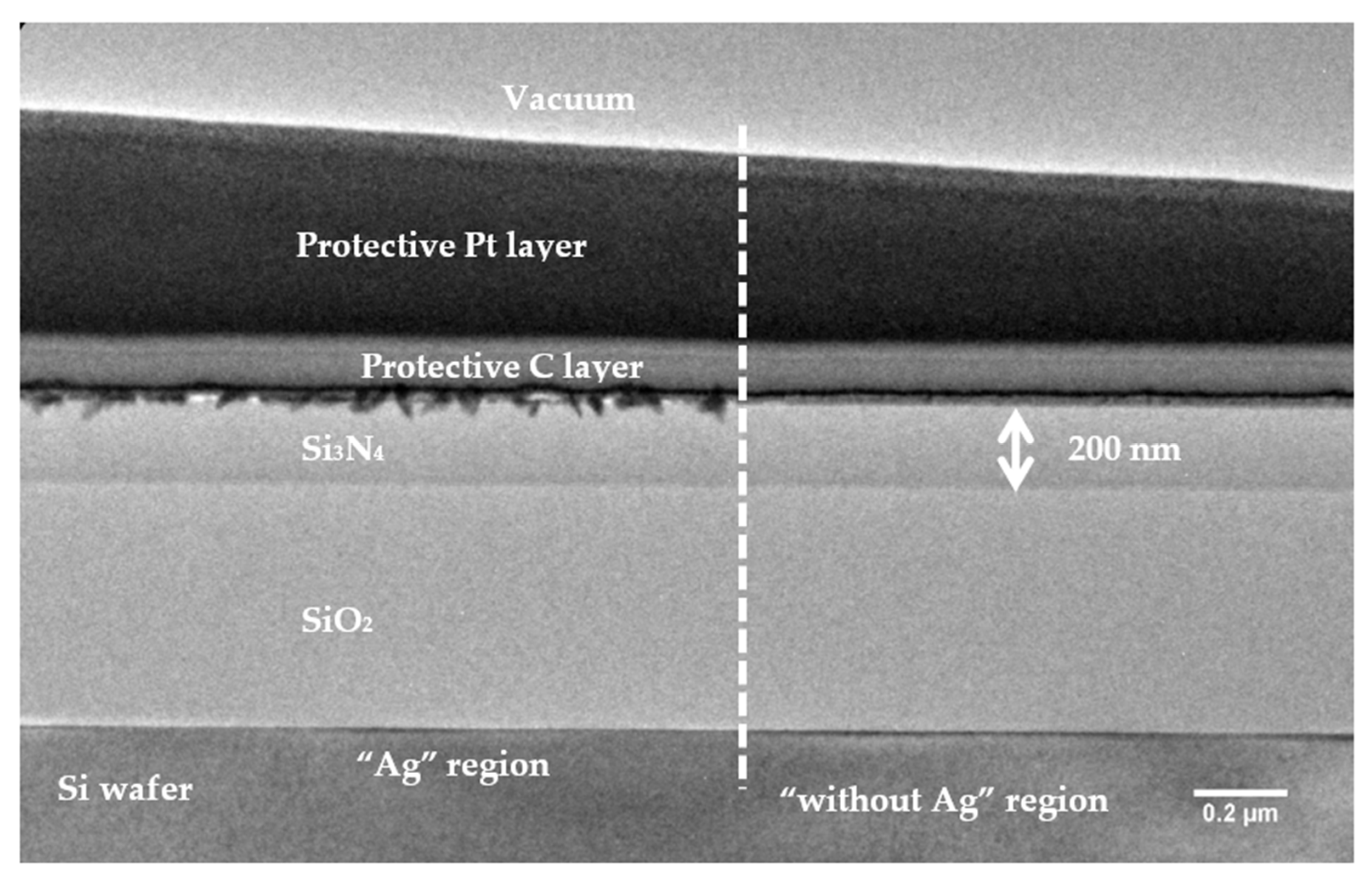
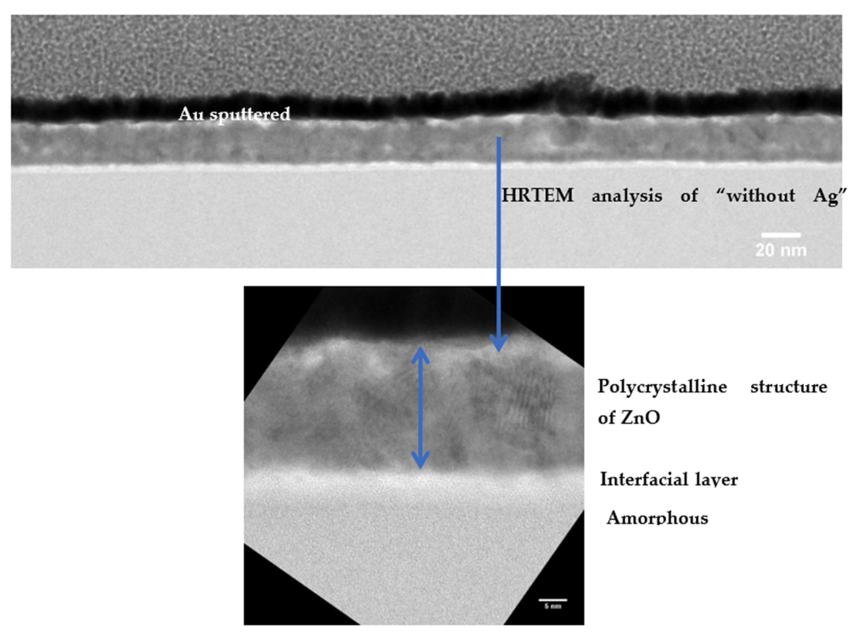
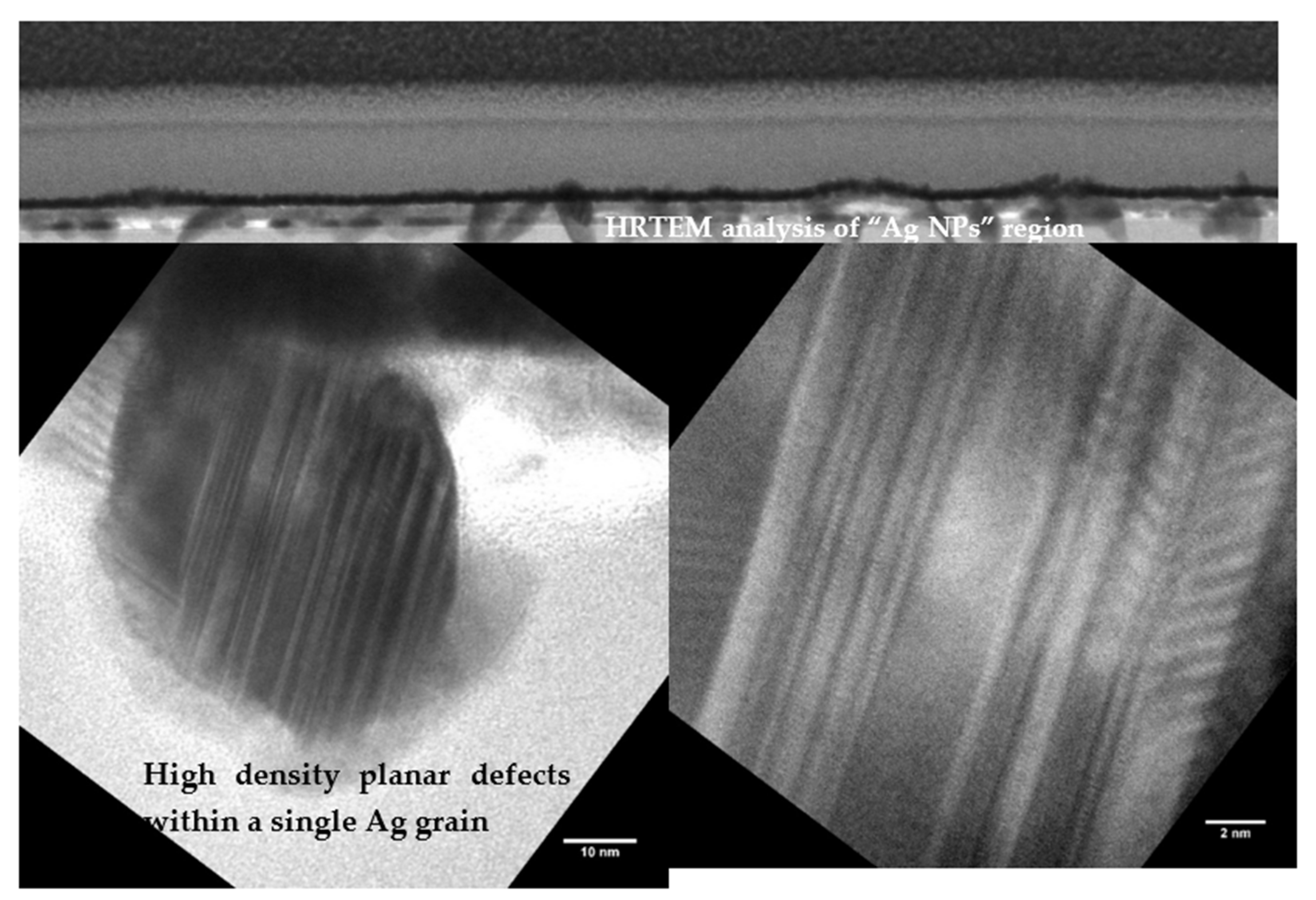
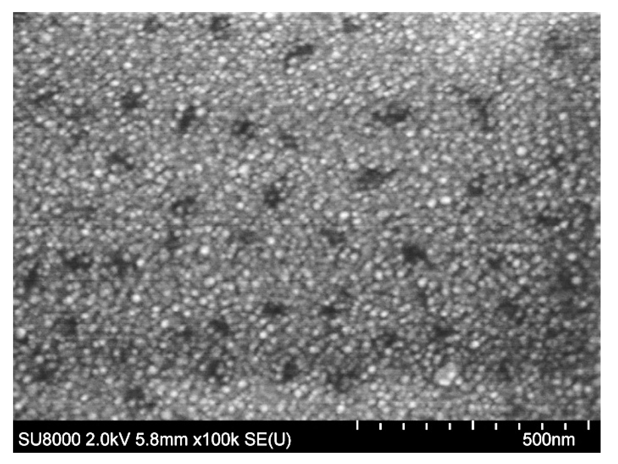
3.3. Morphology of the Ag Layer and Nanolaminate Structure

As the presence of silver particles contributes significantly to the improved conductivity of the nanolaminate structures, we have investigated the morphology of the silver layer and its surface topography. Figure 5 shows an AFM image of the silicon surface whereby the silver is deposited through a mask.
Figure 6a,b show the 3D and plain AFM images of sputtered Ag on Si substrate after 7 s and 15 s sputtering time. It is clear that the continuous Ag layer was not formed after magnetron sputtering according to the morphology images in Figure 7 and Figure 8. The Ag nanoclusters are randomly distributed with distinct shapes and sizes, forming isolated crystal grains. The diameter of the Ag particles is about 30–50 nm. As the sputtering time of the Ag layer is increased, the size (diameter) of the Ag particles is also increased, but their height did not change obviously. From the AFM measurement, the RMS roughness, the arithmetic average roughness Ra and the maximum roughness depth of samples were determined. For the shorter deposition time (7 s), the Ag layer has the following surface parameters: RMS is 3.04 nm, Ra is 2.03 nm, and Rmax is 26.8 nm. Interestingly, the increase of the deposition time to 15 sec results in lower surface parameters: RMS is 2.32 nm, Ra is 1.73 nm, and Rmax is 21.2 nm. Similar results were also reported for the deposition of copper nanoclusters [8].
The film morphology of silver was studied by the HRTEM method. For this purpose, the substrate used was an oxidized silicon wafer, coated with silicon nitride (200 nm) for consecutive deposition of ZnO and Ag, whereby the latter was sputtered for 7 s. The deposition was made through a mask to define areas with and without silver particles within the same sample for analysis. Finally, a top blanket layer of ZnO was deposited. The nanolaminate structure was investigated with cross-section TEM and the images are shown in Figure 7, Figure 8 and Figure 9, whereby lower magnification (larger imaging area) images are resented in Figure 7 outlining the difference between regions with and without Ag nano-granules. Higher magnification images of these two regions are presented in Figure 8 and Figure 9, respectively.
The polycrystalline structure of the consecutively sputtered ZnO layers is clearly distinguished (as can be seen in Figure 8).
In comparison, the region with Ag NPs shows that the sputtering for 7 sec results in forming of a discontinuous film with Ag nanoparticles with a random in-plane orientation as well as a size of about 100 nm. These 3D nanoclusters have penetrated into the ZnO film and even into the underlying Si3N4 layer (Figure 9). The dark and bright bands in the Ag nanoclusters are twinning or multiple stacking faults. This is typical for Ag nano-granules when it is formed at low temperature.
Figure 10 shows an SEM image of nanolaminate structure ZnO (29 nm)/Ag (7 sec)/ZnO (29 nm). The Ag islands are clearly seen. This result agrees with AFM and TEM analysis.
The most important part of the technological process of nanolaminate (OMO) structure with specified optical and electrical properties is the deposition of the discontinuous metal layer. The optical properties and electrical conductivity are modified with planar-located metal granules.
Usually, TCOs have a semiconductor behavior as a negative temperature coefficient of receptivity (TCR). The nanolaminate structure with metal granulate demonstrates metallic conductivity because it has a positive TCR [15]. Therefore, the carriers are delocalized due to thermal activation, and conductivity is dominated by phonon scattering.
Our hypothesis is based on the usage of electronic conductivity in granular (discontinuous) type materials [13]. The key parameter that determines most of the physical properties of the granular array is the average tunneling conductance G between neighboring grains. It is convenient to introduce the dimensionless conductance [13], (corresponding to one spin component):
g = G ( 2 e 2 h ) ,
which is measured in units of the quantum conductance (e2/h). The samples with g>1 exhibit metallic transport properties, while those with g < 1 show insulating behavior.
This hypothesis is confirmed by using the OMO structure as a strain resistor [16,41,42].The exponential dependence of the tunneling probability on the intergranular distance suggests the suitability of the material as a high-sensitivity strain sensor. When the OMO nanolaminate structure is strained in tension, the average distance between the particles increases. The tunneling probability decreases, and the resistivity of the microresistor increases [41].

3.4. Effect of Temperature Annealing

The impact of the thermal treatment on the optical and electrical properties of sample 2—ZnO (29 nm)/Ag (7 sec)/ZnO (63 nm)—was studied. When sample 2 was exposed to low-temperature annealing at 200 °C/30 min, the transparency and the sheet resistance were almost unchanged, however, when treated at 400 °C/15 min, the transmittance is reduced by 10 to 15% to an average transmittance of 84.6% in the spectral range of 400–800 nm (see Figure 11). In parallel, the measured sheet resistance is changed from 8 to 20 Ω/sq and correspondingly, the FOM was significantly decreased to 10.57 × 10⁻³ Ω−1.
The sheet resistance is relatively low and the nanolaminate structure is still transparent. These results are encouraging as they suppose a kind of stability during thermal treatments. This is an advantage for applying these structures as optical contacts in devices where thermal treatments are required.

4. Conclusions

In conclusion, we have demonstrated highly efficient transparent ZnO/Ag/ZnO structures deposited at room temperature which are especially suitable for the application as the TCO layer.The selected technological conditions for magnetron sputtering of silver led to the formation of a discontinuous layer of Ag nanoclusters and these clusters define the optical and electrical properties of ZnO/Ag/ZnO nanolaminate structures. The technological process for sputtering Ag is reproducible and reliable in terms of thickness and structure. This has been proven on the basis of 10 years of experimental experience. This study also presents two indirect methods for detecting the presence of silver nanoclusters:spectroscopic ellipsometry and TEM analysis. In order to achieve superior optical transparency and low sheet resistance, the crucial role has not only the sputtering process of Ag but the optimal film thickness of the ZnO top layer as well. Varying ZnO layer thickness, the figure of merit (FOM) changes from 16.64 × 10⁻³ to 111.01 × 10⁻³Ω−1.The optimized ZnO/Ag/ZnO structure achieves a maximum transmittance of 98% (550 nm) and sheet resistance of 8 Ω/sq.After low-temperature annealing at 200°C/30 min, the transparency and the sheet resistance were almost unchanged. In order to achieve superior optical transparency and low sheet resistance, the crucial role has not only the sputtering process of Ag but the optimal film thickness of the ZnO top layer as well. The optimized oxide/metal/oxide structure achieves a maximum transmittance of 98% (550 nm) and sheet resistance of 8 Ω/sq.
The advantage of the proposed multisource magnetron sputtering deposition of nanolaminate structures is that the formation is performed at room temperature and at a relatively high deposition rate of nearly 9.9 nm/min. This makes the proposed approach for the fabrication of TCO coatings easily applicable for lab-scale and commercial devices. This technological process can be applied to flexible substrates as well.

Author Contributions

P.V.: conceptualization, writing—original draft preparation, supervision; T.I.: investigation, writing—original draft preparation, writing—review and editing; H.D.: investigation, Validation; P.T.: investigation; M.G.: investigation; N.P.: investigation, writing—review and editing; Y.G.: investigation, writing—review and editing; A.A.: supervision. All authors have read and agreed to the published version of the manuscript.

Funding

The authors kindly acknowledge financial support from project № BG05M2OP001-1.002-0014 “Center of competence HITMOBIL—Technologies and systems for generation, storage and consumption of clean energy”, funded by Operational Programme “Science and Education For Smart Growth” 2014–2020, co-funded by the EU from European Regional Development Fund.

Institutional Review Board Statement

Not applicable.

Informed Consent Statement

Not applicable.

Data Availability Statement

The data are not publicly available.

Acknowledgments

The authors kindly acknowledge financial support from project № BG05M2OP001-1.002-0014 “Center of competence HITMOBIL—Technologies and systems for generation, storage and consumption of clean energy”, funded by Operational Programme “Science and Education For Smart Growth” 2014–2020, co-funded by the EU from European Regional Development Fund.

Conflicts of Interest

The authors declare no conflict of interest.

References

  1. Sharma, V. Transparent conducting electrodes based on zinc oxide. In Metal Oxides, Nanostructured Zinc Oxide; Awasthi, K., Ed.; Elsevier: Amsterdam, The Netherlands, 2021; pp. 291–318. [Google Scholar]
  2. Singh, R.; Gupta, M.; Mukherjee, S.K. Effect of Ag layer thickness on optical and electrical properties of ion-beam-sputtered TiO2/Ag/TiO2 multilayer thin film. J.Mater. Sci Mater.Electron. 2022, 33, 6942–6953. [Google Scholar] [CrossRef]
  3. Barman, B.; Kumar, S.; Dutta, K.S. Fabrication of highly conducting ZnO/Ag/ZnO and AZO/Ag/AZO transparent conducting oxide layers using RF magnetron sputtering at room temperature. Mater. Sci. Semicond. Process. 2021, 129, 105801. [Google Scholar] [CrossRef]
  4. Nezhad, E.H.; Haratizadeh, H.; Kari, B.M. Influence of Ag mid-layer in the optical and thermal properties of ZnO/Ag/ZnO thin films on the glass used in Buildings as insulating glass unit (IGU). Ceram. Int. 2019, 45, 9950–9954. [Google Scholar] [CrossRef]
  5. Miao, D.; Jiang, S.; Shang, S.; Chen, Z. Highly transparent and infrared reflective AZO/Ag/AZO multilayer film prepared on PET substrate by RF magnetron sputtering. Vacuum 2014, 106, 1–4. [Google Scholar] [CrossRef]
  6. Sahu, D.R.; Huang, J.L. High quality transparent conductive ZnO/Ag/ZnO multilayer films deposited at room temperature. Thin Solid Films 2006, 515, 876–879. [Google Scholar] [CrossRef]
  7. Sahu, D.R.; Lin, S.Y.; Huang, J.L. ZnO/Ag/ZnO multilayer films for the application of a very low resistance transparent electrode. Appl. Surf. Sci. 2006, 252, 7509–7514. [Google Scholar] [CrossRef]
  8. Song, S.; Yang, T.; Lv, M.; Li, Y.; Xin, Y.; Jiang, L.; Wu, Z.; Han, S. Effect of Cu layer thickness on the structural, optical and electrical properties of AZO/Cu/AZO tri-layer films. Vacuum 2010, 85, 39–44. [Google Scholar] [CrossRef]
  9. Kim, J.H.; Moon, Y.J.; Kim, S.K.; Yoo, Y.Z.; Seong, T.Y. Al-doped ZnO/Ag/Al-doped ZnO multilayer films with a high figure of merit. Ceram. Int. 2015, 41, 14805–14810. [Google Scholar] [CrossRef]
  10. Jeon, K.; Youn, H.; Kim, S.; Shin, S.; Yang, M. Fabrication and characterization of WO3/Ag/WO3 multilayer transparent anode with solution-processed WO3 for polymer light-emitting diodes. Nanoscale Res. Lett. 2012, 7, 253. [Google Scholar] [CrossRef]
  11. Yu, S.; Zhang, W.; Li, L.; Xu, D.; Dong, H.; Jin, Y. Optimization of SnO2/Ag/SnO2 tri-layer films as transparent composite electrode with high figure of merit. Thin Solid Films 2014, 552, 150–154. [Google Scholar] [CrossRef]
  12. Kim, J.H.; Kim, D.H.; Seong, T.Y. Realization of highly transparent and low resistance TiO2/Ag/TiO2 conducting electrode for optoelectronic devices. Ceram. Int. 2015, 41, 3064–3068. [Google Scholar] [CrossRef]
  13. Beloborodov, I.S.; Lopatin, A.V.; Vinokur, V.M.; Efetov, K.B. Granular electronic system. Rev. Mod. Phys. 2007, 79, 469–518. [Google Scholar] [CrossRef]
  14. Dikov, H.; Ivanova, T.; Vitanov, P. Oxide/metal/oxide nanolaminate structures for application of transparent electrodes. J. Phys. Conf. Ser. 2016, 764, 012021. [Google Scholar] [CrossRef]
  15. Dikov, H.; Vitanov, P.; Ivanova, T.; Stavrov, V. Optical and electrical properties of nanolaminate dielectric structures. J. Phys. Conf. Ser. 2016, 700, 012054. [Google Scholar] [CrossRef]
  16. Dikov, C.; Vitanov, P.; Ivanova, T.; Stavrov, V.; Tomerov, E.; Stavreva, G.; Bineva, I. Optical and electrical properties of TiO2/Pt/TiO2 nanolaminate structures. J. Phys. Conf. Ser. 2018, 992, 012033. [Google Scholar] [CrossRef]
  17. Su, Y.C.; Chiou, C.C.; Marinova, V.; Lin, S.H.; Dikov, H.; Vitanov, P.; Hsu, K.Y. Liquid crystal electro-optic modulator based on transparent conductive TiO2/Ag/TiO2 multilayers. Opt. Quant. Electron. 2018, 50, 242. [Google Scholar] [CrossRef]
  18. Chiou, C.C.; Hsu, F.H.; Petrov, S.; Marinova, V.; Dikov, H.; Vitanov, P.; Lin, S.H. Flexible light valves using polymer-dispersed liquid crystals and TiO2/Ag/TiO2 multilayers. Opt. Express 2019, 21, 1691. [Google Scholar] [CrossRef]
  19. Yu, X.; Zhang, D.; Wang, P.; Murakami, R.; Ding, B.; Song, X. The optical and electrical properties of ZnO/Ag/ZnO films on flexible substrate. Int. J. Modern Phys. Conf. Ser. 2012, 6, 55–56. [Google Scholar] [CrossRef]
  20. Zhao, Z.; Alford, T.L. The optimal TiO2/Ag/TiO2 electrode for organic solar cell application with high device-specific Haacke figure of merit. Sol. Energy Mater. Sol. Cells 2016, 157, 599–603. [Google Scholar] [CrossRef]
  21. Al-Kuhaili, M.F.; Durrani, S.M.A.; El-Said, A.S.; Heller, R. Enhancement of the refractive index of sputtered zinc oxide thin films through doping with Fe2O3. J. Alloys Compd. 2017, 690, 453–460. [Google Scholar] [CrossRef]
  22. Sytchkova, A.; Grilli, M.L.; Rinaldi, A.; Vedraine, S.; Torchio, P.; Piegari, A.; Flory, F. Radio frequency sputtered Al:ZnO-Ag transparent conductor: A plasmonic nanostructure with enhanced optical and electrical properties. J. Appl. Phys. 2013, 114, 094509. [Google Scholar] [CrossRef]
  23. Haacke, G. New figure of merit for transparent conductors. J. Appl. Phys. 1976, 47, 4086. [Google Scholar] [CrossRef]
  24. Bou, A.; Torchio, P.; Vedraine, S.; Barakel, D.; Lucas, B.; Bernède, J.C.; Thoulon, P.Y.; Ricci, M. Numerical optimization of multilayer electrodes without indium for use in organic solar cells. Sol. Energy Mater. Sol. Cells 2014, 125, 310–317. [Google Scholar] [CrossRef]
  25. Kim, G.; Lim, J.W.; Lee, J.; Heo, S.J. Flexible multilayered transparent electrodes with less than 50 nm thickness using nitrogen-doped silver layers for flexible heaters, Mater. Res. Bull. 2022, 149, 111703. [Google Scholar] [CrossRef]
  26. Rabizadeh, M.; Ehsani, M.H. Effect of heat treatment on optical, electrical and thermal properties of ZnO/Cu/ZnO thin films for energy-saving application. Ceram. Int. 2022, 48, 16108–16113. [Google Scholar] [CrossRef]
  27. Kim, J.H.; Lee, J.H.; Kim, S.W.; Yoo, Y.Z.; Seong, T.Y. Highly flexible ZnO/Ag/ZnO conducting electrode for organic photonic devices. Ceram. Int. 2015, 41, 7146–7150. [Google Scholar] [CrossRef]
  28. El Hajj, A.; Lucas, B.; Chakaroun, M.; Antony, R.; Ratier, B.; Aldissi, M. Optimization of ZnO/Ag/ZnO multilayer electrodes obtained by Ion Beam Sputtering for optoelectronic devices. Thin Solid Films 2012, 520, 4666–4668. [Google Scholar] [CrossRef]
  29. Zhang, Y.; Liu, Z.; Ji, C.; Chen, X.; Hou, G.; Li, Y.; Zhang, X. Low-Temperature Oxide/Metal/Oxide Multilayer Films as Highly Transparent Conductive Electrodes for Optoelectronic Devices. ACS Appl. Energy Mater. 2021, 4, 6553–6561. [Google Scholar] [CrossRef]
  30. Chu, C.H.; Wu, H.W.; Huang, J.L. AZO/Au/AZO tri-layer thin films for the very low resistivity transparent electrode applications. Mater. Sci. Eng. B 2014, 186, 117–121. [Google Scholar] [CrossRef]
  31. Mendil, D.; Challali, F.; Touam, T.; Bockelée, V.; Ouhenia, S.; Souici, A.; Djouadi, D.; Chelouche, A. Preparation of RF sputtered AZO/Cu/AZO multilayer films and the investigation of Cu thickness and substrate effects on their microstructural and optoelectronic properties. J. Alloys Compd. 2021, 860, 158470. [Google Scholar] [CrossRef]
  32. Lee, S.Y.; Park, Y.S.; Seong, T.Y. Optimized ITO/Ag/ITO multilayers as a current spreading layer to enhance the light output of ultraviolet light-emitting diodes. J. Alloys Compd. 2019, 776, 960–964. [Google Scholar] [CrossRef]
  33. Im, H.S.; Kim, S.K.; Lee, T.J.; Seong, T.Y. Combined effects of oxygen pressures and RF powers on the electrical characteristics of ITO-based multilayer transparent electrodes. Vacuum 2019, 169, 108871. [Google Scholar] [CrossRef]
  34. Li, H.; Gao, Y.J.; Yuan, S.H.; Wuu, D.S.; Wu, W.Y.; Zhang, S. Improvement in the figure of merit of ITO-Metal-ITO sandwiched films on poly substrate by high-power impulse magnetron sputtering. Coatings 2021, 11, 144. [Google Scholar] [CrossRef]
  35. Wu, C.C. High flexible touch screen panel fabricated with silver-inserted transparent ITO triple-layer structures. RSC Adv. 2018, 8, 11862–11870. [Google Scholar] [CrossRef] [PubMed]
  36. Song, T.S.; Cho, J.W.; Kim, J.H.; Kim, S.K.; Seong, T.Y. High ultraviolet transparent conducting electrodes formed using tantalum oxide/Ag multilayer. Ceram. Int. 2022, 48, 3536–3543. [Google Scholar] [CrossRef]
  37. Wang, P.; Zhang, D.; Kim, D.H.; Qiu, Z.; Gao, L.; Murakami, R.; Song, X. Enhancement of light transmission by coupling to surface plasmon polaritons of a layer-plus-islands silver layer. J. Appl. Phys. 2009, 106, 103104. [Google Scholar] [CrossRef]
  38. Shafiq, R.; Khan, A.D.; Al-Harbi, F.F.; Ali, F.; Armghan, A.; Asif, M.; Rehman, A.U.; Ali, F.; Arpanaei, E.M.; Alibakhshikenari, M. Optical Transmission Plasmonic Color Filter with Wider Color Gamut Based on X-Shaped Nanostructure. Photonics 2022, 9, 209. [Google Scholar] [CrossRef]
  39. Huang, Y.; Fang, Y.; Zhang, Z.; Zhu, L.; Sun, M. Nanowire-supported plasmonic waveguide for remote excitation of surface-enhanced Raman scattering. Light Sci. Appl. 2014, 3, e199. [Google Scholar] [CrossRef]
  40. Zhang, D.; Yabe, H.; Akita, E.; Wang, P.; Murakami, R.; Song, X. Effect of silver evolution on conductivity and transmittance of ZnO/Ag thin films. J. Appl. Phys. 2011, 109, 104318. [Google Scholar]
  41. Stavrov, V.; Stavreva, G.; Tomerov, E.; Dikov, H.; Vitanov, P. Self-sensing cantilevers with nano-laminated Dielectric-Metal-Dielectric resistors. In Proceedings of the 2017 40th International Spring Seminar on Electronics Technology (ISSE), Sofia, Bulgaria, 10–14 May 2017; pp. 1–6. [Google Scholar]
  42. Dukic, M.; Winhold, M.; Schwalb, C.; Adams, J.D.; Stavrov, V.; Huth, M.; Fantner, G.E. Direct-write nanoscale printing of nanogranular tunnelling strain sensors for sub-micrometre cantilevers. Nat. Commun. 2016, 7, 12487. [Google Scholar] [CrossRef] [Green Version]
Figure 1. Dispersion of (a) refractive index and (b) extinction coefficients of magnetron sputtered ZnO/ZnO structures, sample 4 and sample 5.
Coatings 12 01324 g001
Figure 2. Ellipsometric angles (Ψ, Δ) of (a) sample 1 (ZnO (29 nm)/Ag (7 sec)/ZnO (29 nm)), sample 3 (ZnO (29 nm)/Ag (10 sec)/ZnO (29 nm)), and (b) sample 4 (ZnO (29 nm)/ZnO (29 nm)) on glass substrate. Ψand Δ are measured at an angle of incidence of 45°.
Coatings 12 01324 g002
Figure 3. Transmittance spectra for ZnO/ZnO and nanolaminate structure ZnO/Ag/ZnO. The bare substrate is given for comparison.
Coatings 12 01324 g003
Figure 4. (a) presents the absorption edge of samples with the top and bottom ZnO layers having the same thickness of 29 nm, but the Ag sputtering time has been changed and (b) is the comparison between sample 2, ZnO (29 nm)/Ag (7 s)/ZnO (63 nm)and sample 5, ZnO (29 nm)/ZnO (63 nm).
Coatings 12 01324 g004
Figure 5. A3D AFM image of sputtered Ag on Si through the mask, the border mask/Ag is clearly seen.
Coatings 12 01324 g005
Figure 6. Surface topography of Ag layer after (a) 7 s and (b) 15 s sputtering time.
Coatings 12 01324 g006
Figure 7. TEM cross-section micrograph of the nanolaminate structure with two areas: the “Ag” region is with Ag nano-granules and the “without Ag” region is without Ag deposition.
Coatings 12 01324 g007
Figure 8. TEM cross-section image of the “without Ag” region without Ag granules and the polycrystalline structure of the ZnO layer.
Coatings 12 01324 g008
Figure 9. TEM cross-section of the “Ag granules” region and image of a single Ag granule with planar defects.
Coatings 12 01324 g009
Figure 10. SEM image of the nanolaminate structure ZnO (29 nm)/Ag (7 s)/ZnO (29 nm).
Coatings 12 01324 g010
Figure 11. Transmittance spectra of the as-deposited and the annealed at 400°C/15 min. Sample 2: ZnO (29 nm)/Ag (7 s)/ZnO (63 nm).
Coatings 12 01324 g011
Table 1. The sample preparation and the obtained film thickness of the nanolaminate structure.
SampleSputtering TimeLayer Thickness (nm)
ZnO
(Bottom)
AgZnO (Top)ZnO
(Bottom)
AgZnO (Top)
1ZnO/Ag/ZnO3 min7 s3 min29Nanoclusters29
2ZnO/Ag/ZnO3 min7 s6 min2963
3ZnO/Ag/ZnO3 min10 s3 min2929
4ZnO/ZnO3 min-3 min29 29
5ZnO/ZnO3 min-6 min29 63
Table 2. Sheet resistance, Rsheet, of nanolaminate structures, average transmittance, Taverage, and FOM values, estimated for nanolaminate structures. The average transmittance is determined for the spectral range of 400–800 nm and extracting the substrate transmittance.
StructureRsheet
(Ω/sq)
Taverage
(%)
FOM × 10−3
( Ω 1 )
Sample 1 ZnO (29 nm)/Ag (7 s)/ZnO (29 nm)2390.8416.64
Sample 2 ZnO (29 nm)/Ag (7 s)/ZnO (63 nm)898.82111.01
Sample 3 ZnO (29 nm)/Ag (10 s)/ZnO (29 nm)1394.0141.48
Table 3. Overview of different OMO structures, including their deposition method, average transmittance, sheet resistance, and figure of merit (FOM).
StructuresDeposition MethodRsheet
(Ω/sq)
Taverage
(%)
FOM× 10−3
−1)
Reference
ZnO/Cu/ZnORF/DC sputtering14.0468 (550 nm)63.7[26]
ZnO/Ag/ZnORF/DC sputtering3.0190236[6]
ZnO/Ag/ZnORF sputtering PET substrate4.9892–95104.5[27]
ZnO/Ag/ZnOReactive sputtering825.324[28]
MGZO/Ag/MGZOreactive plasma deposition10.094.758.0[29]
ZnO/Ag/ZnORF sputtering5.487.022.4[3]
AZO/Ag/AZO5.392.045.5[3]
AZO/Au/AZORF sputtering14.3182.1 (550 nm)9.69[30]
AZO/Cu/AZORF sputtering143.4701.97[31]
ITO/Ag/ITOMOCVD3.891.3106.1[32]
ITO/Ag/ITORF sputtering264.392.01.65[33]
ITO/Ag/ITOImpulse magnetron sputtering7.2997.0101.16[34]
ITO/Cu/ITO10.4374.04.83[34]
TiO2/Ag/TiO2RF sputtering3.58969.6[33]
TiO2/Ag/TiO2RF sputtering3.3196.869.6[9]
TiO2/Ag/TiO2sputtering1388.7 (550 nm)23.2[35]
SnO2/Ag/SnO2RF sputtering9.094.860.0[11]
Ta2O5/Ag/Ta2O5RF sputtering2.5391.64157.04[36]
Publisher’s Note: MDPI stays neutral with regard to jurisdictional claims in published maps and institutional affiliations.

