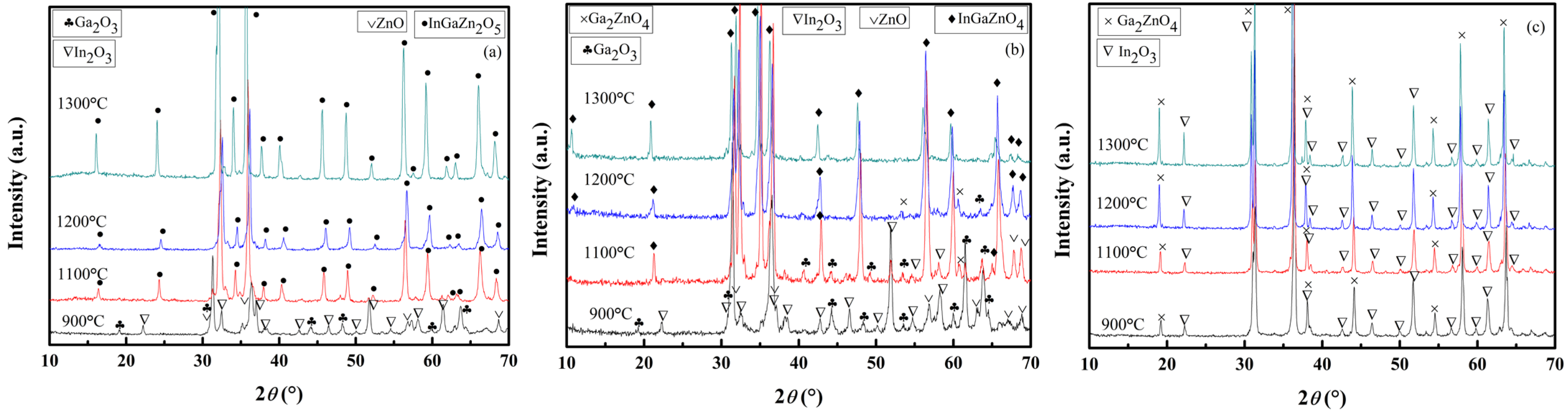
3.1. Characterization of the IGZO Sputtering Targets
Figure 2a–c presents the XRD profiles of the IGZO targets with various Ga content ratios sintered in temperatures of 900 °C to 1300 °C for 6 or 8 h. According to Joint Committee of Powder Diffraction Standard (JCPDS) files nos. 400,252 and 381,104, both the InGaZn
2O
5 and the InGaZnO
4 targets are of single-phase structure when the sintering temperature reaches 1300 °C, as shown in
Figure 2a,b. However, the XRD pattern of the InGa
2ZnO
5.5 target shown in
Figure 2c indicates that it contains two phases, i.e., Ga
2ZnO
4 and In
2O
3, in accord with the JCPDS files nos. 860,410 and 060,416. Hence, the InGa
2ZnO
5.5 target sintered at the temperature of 1300 °C is of two-phase structure.
Figure 2a,b illustrates that the IGZO targets remain as the mixtures of raw powders at a temperature of 900 °C. According to
Figure 2a, the InGaZn
2O
5 phase formed in InGaZn
2O
5 target at 1100 °C via the following reaction:
Figure 2b shows that at 1100 °C the cubic spinel Ga
2ZnO
4 and the rhombohedral InGaZnO
4 phases emerged in the InGaZnO
4 target according to the following reactions:
With the increase in sintering temperature, the Ga2ZnO4 reacted with the remaining raw powders to form the InGaZnO4 phase, and the InGaZnO4 target became the single-phase structure at 1300 °C.
For the InGa2ZnO5.5 target, the Ga2O3 and ZnO reacted to form Ga2ZnO4 phases at 900 °C. In2O3 acted as an inert component during the sintering treatment of the InGa2ZnO5.5 target up to 1300 °C and, hence, the two phases, In2O3 and Ga2ZnO4, comprised the InGa2ZnO5.5 target.
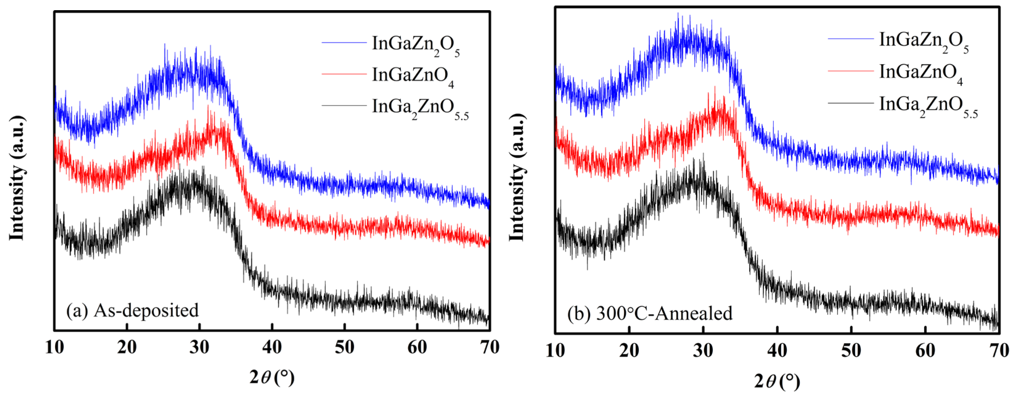
3.2. Characterization of a-IGZO Channel Layers
The IGZO layers were deposited using self-prepared IGZO targets with various Ga content ratios.
Figure 3a,b shows the XRD patterns of the as-deposited IGZO layers and the IGZO layers subjected to annealing at 300 °C for 1 h in an ambient atmosphere. Regardless of whether annealing treatment was carried out or not, the characteristic diffraction peaks were absent for the three types of IGZO layers in the 2
θ range of 10° to 70°. The analytical results indicate that the phase structures of the IGZO sputtering targets and the post-annealing have no effect on the amorphism of the IGZO layers prepared in this study [
16].
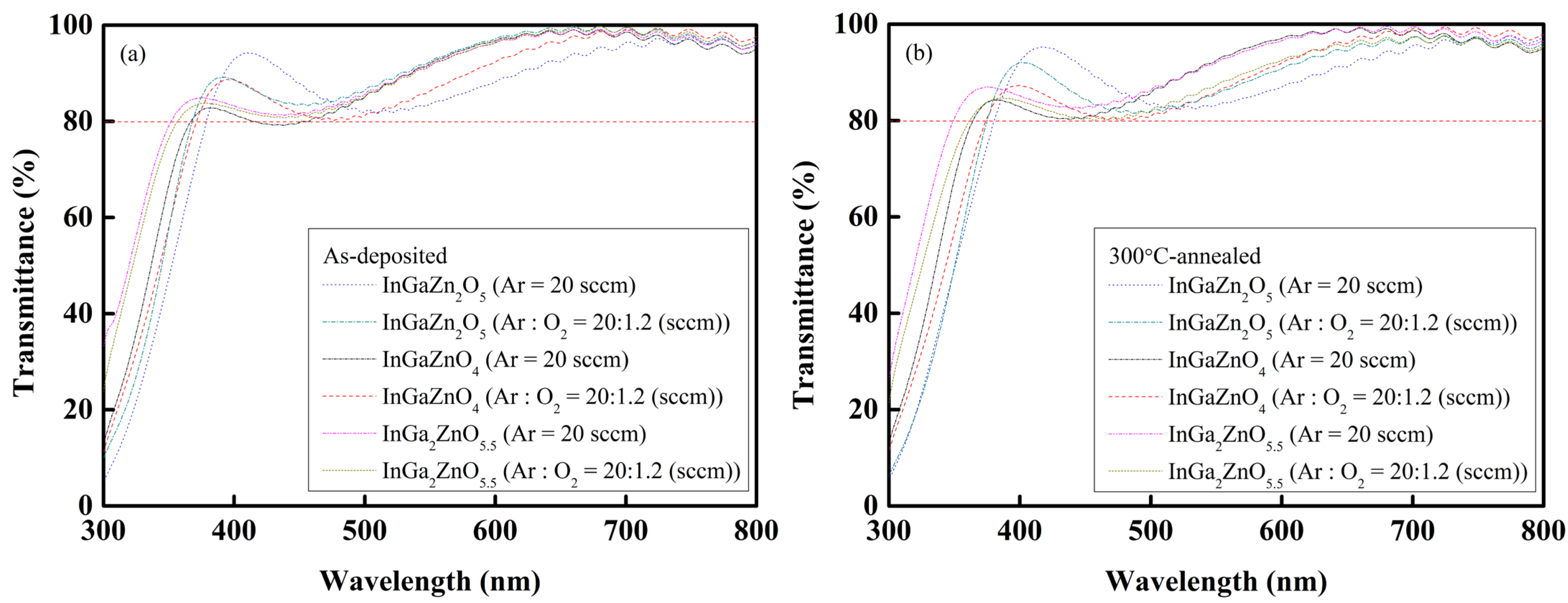
Figure 4a,b shows the transmittance spectra of the
a-IGZO layers in the visible-light wavelength range of 300 to 800 nm. The transmittances are greater than 80%, and there is no significant difference in transmittances for all the types of
a-IGZO layers. The types and ratios of gas flow rates for the sputtering deposition also show little influence on the transmittances of the
a-IGZO layers prepared in this study.
Figure 4a,b also reveals the shift in the transmittance spectra of the
a-IGZO layers, and this was found to relate to the Ga content of the
a-IGZO layers.
Figure 5a,b sketches the (
αhν)
2 versus
hν plots extracted from the transmittance spectra, and the Tauc’s method [
17] was employed to determine the values of the energy bandgap (
Eg’s) of the
a-IGZO layers. The analytical results indicated that the
Eg value increased with the increase in the Ga content of the
a-IGZO layers. For instance, in the 300 °C-annealed samples deposited without oxygen incorporation, the
Eg’s of the
a-InGaZn
2O
5,
a-InGaZnO
4, and
a-InGa
2ZnO
5.5 layers were separately equal to 3.73, 3.98, and 4.03 eV. This is ascribable to the strong bonding feature of the Ga
3+ ions which, in turn, limits the motion of charge carriers in the
a-IGZO layers. In other words, the enlargement of the
Eg value of an
a-IGZO layer due to the increase in Ga content predicts that the charge carriers will be more difficult to migrate in an
a-IGZO layer with high Ga content.
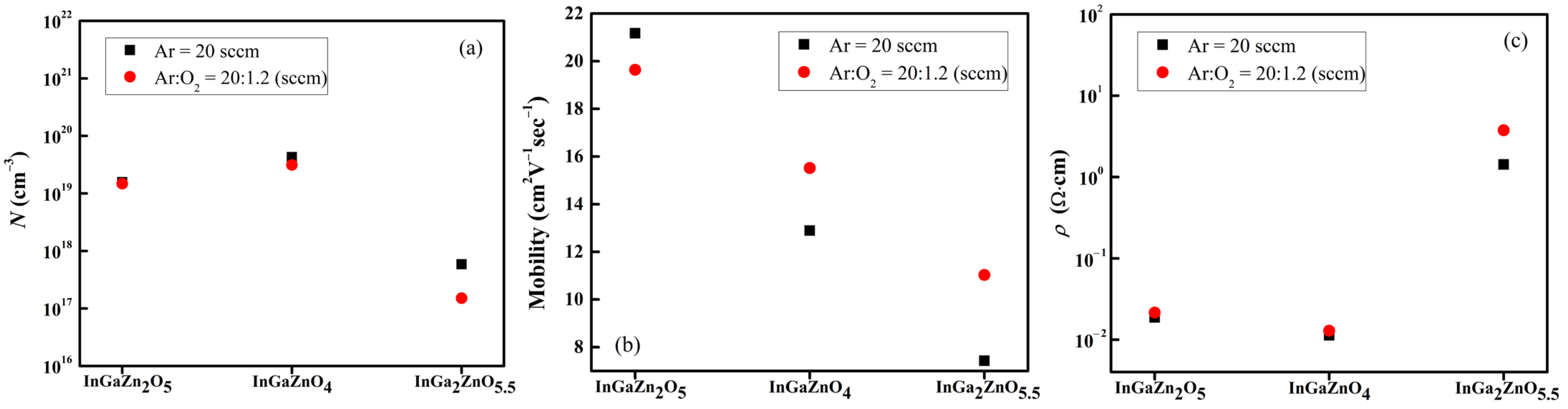
Figure 6a–c depicts the
N,
μHall, and
ρ of various
a-IGZO layers deposited with the gas flow rates of Ar = 20 sccm, and Ar:O
2 = 20:1.2 (sccm), and their values are listed in
Table 2 and
Table 3. The Hall effect measurement revealed that all the
a-IGZO layers are of the
n-type and, with the increase in Ga content, the
N and
μHall decrease whereas the
ρ increases. Hosono has reported that, due to the relatively small ionic radius, the Ga
3+ ions may attract oxygen ions in
a-IGZO layers and thereby suppress the formation of oxygen vacancies [
18]. The oxygen-deficiency reaction in ionic compounds is known to be:
According to the above reaction, the number of electrons decreases with the decrease in oxygen vacancies and thereby the
N decreases with the increase in Ga content in
a-IGZO layers. This is clearly supported by the measured results that the
N’s of the
a-InGaZn
2O
5 and
a-InGaZnO
4 layers are about 10
19 cm
−3 whereas the
N of the
a-InGa
2ZnO
5.5 layer decreases by two orders of magnitude to 10
17 cm
−3. The relatively high valence feature of the Ga
3+ ions may also attract electrons and impede their migration, which explains why the
μHall decreases with the increase in Ga content in the
a-IGZO layers. The electrical conductivity (
σ) can be expressed as:
where
ρ is the electrical resistivity and
e is the electronic charge. As indicated by Equation (5), the decrease in
N and
μHall leads to the increase in
ρ. The results of the Hall effect measurement are hence consistent with the results reported by Hosono [
18].
In this study, oxygen gas was also introduced during the sputtering deposition of the
a-IGZO layers, and its influence on electrical properties of the
a-IGZO layers was investigated.
Figure 6a shows that the
N’s of the
a-IGZO layers deposited without the introduction of oxygen gas are slightly higher than those of the
a-IGZO layers deposited with the introduction of oxygen gas. This is ascribed to the remedy of oxygen deficiencies in the
a-IGZO layers deposited with the introduction of the oxygen gas, which consequently reduced the numbers of oxygen vacancies and charge carriers as depicted by Equation (4). The reduction in charge carriers also caused the escalation of
ρ in the
a-IGZO layers deposited with the introduction of oxygen gas, as shown in
Figure 6c. As to the
μHall,
Figure 6b indicates that the values of
μHall decreased with the increase in Ga content in the
a-IGZO layers regardless of the introduction of the oxygen gas during the sputtering deposition. As revealed by the XRD analysis, all the IGZO layers prepared in this study are amorphous, so that the lattice regularity should have little influence on the
μHall values. It is hence speculated that the difference in Ga content dominates the mobility property of the
a-IGZO layers prepared in this study. As stated above, the high valence feature of the Ga
3+ ions might impede the migration of the charge carriers. The
a-InGaZn
2O
5 layers possesses the lowest Ga content, as listed in
Table 1, implying less obstacles of charge carrier migration induced by Ga
3+ ions and, hence, a high
μHall value for the
a-InGaZn
2O
5 layer. Moreover, the
a-InGaZn
2O
5 layer deposited within Ar = 20 sccm possesses the highest
μHall of 21.17 cm
2·V
−1·sec
−1, which is higher than that of the
a-InGaZn
2O
5 layers deposited with Ar:O
2 = 20:1.2 (sccm) as depicted by
Figure 6b. On the contrary, the sputtering deposition with Ar:O
2 = 20:1.2 (sccm) benefits the
μHall’s of the
a-InGaZnO
4 and
a-InGa
2ZnO
5.5 layers as shown in
Figure 6b. We speculated that the remedy for oxygen deficiencies caused by the introduction of the oxygen gas during the sputtering deposition similarly repairs the interruptions of atom bonds caused by the oxygen vacancies and improves the
μHall’s of the
a-InGaZnO
4 and
a-InGa
2ZnO
5.5 layers.
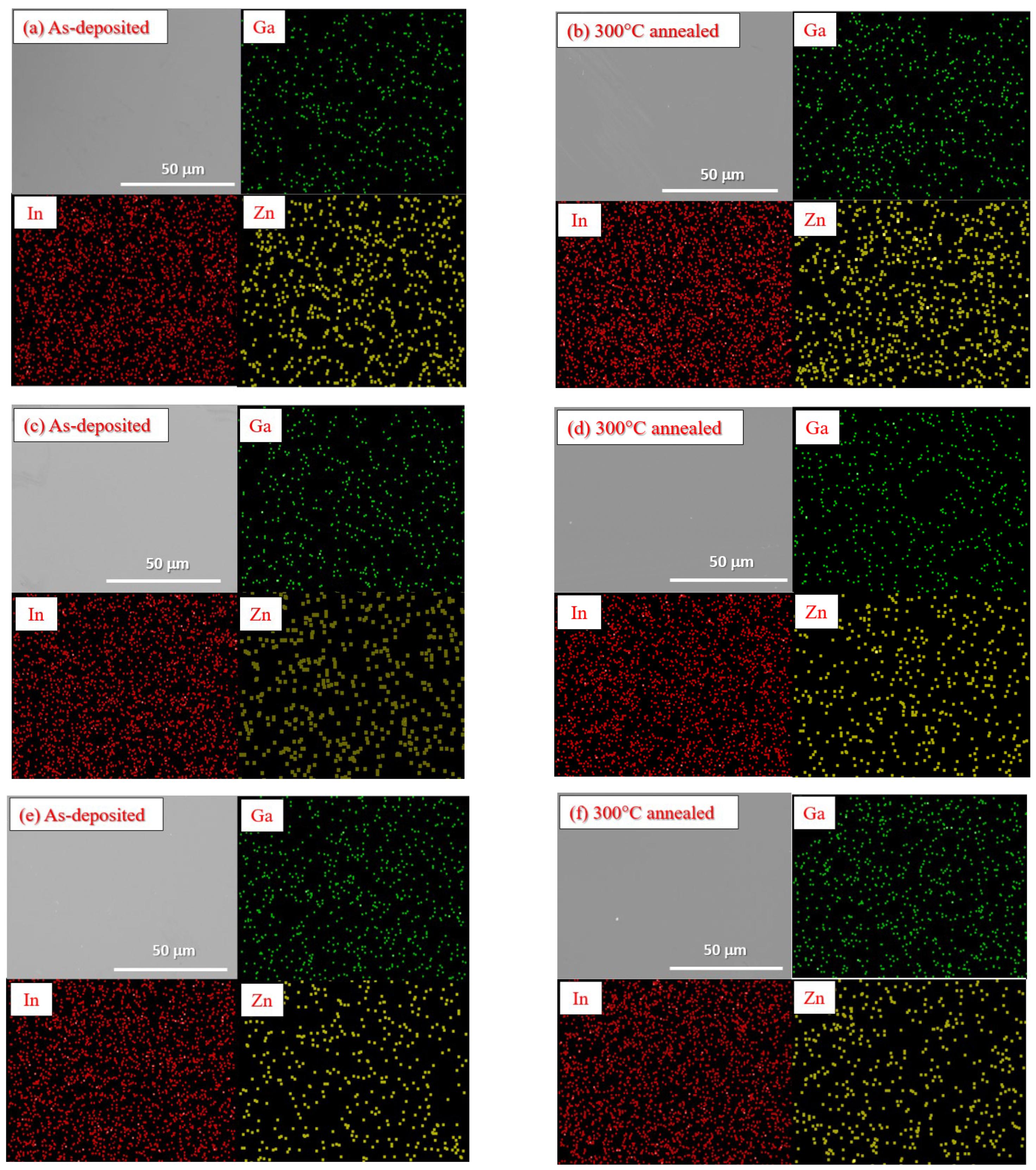
Figure 7a–f presents the SEM micrographs and EDS element mappings of as-deposited and 300 °C-annealed
a-IGZO layers deposited with a gas flow rate of Ar:O
2 = 20:1.2 (sccm). The analytical results of SEM and EDS indicate that all the
a-IGZO layers exhibit flat surfaces with no specific geometric features and uniform In, Ga, and Zn element distributions. As depicted by
Figure 7e,f, element aggregation was absent even in the
a-InGa
2ZnO
5.5 layer prepared by using the double-phase sputtering target. This illustrates that Ga content is indeed the main factor affecting the electrical properties of
a-IGZO layers.
3.3. Electrical Properties of the Three Types of IGZO TFT Devices
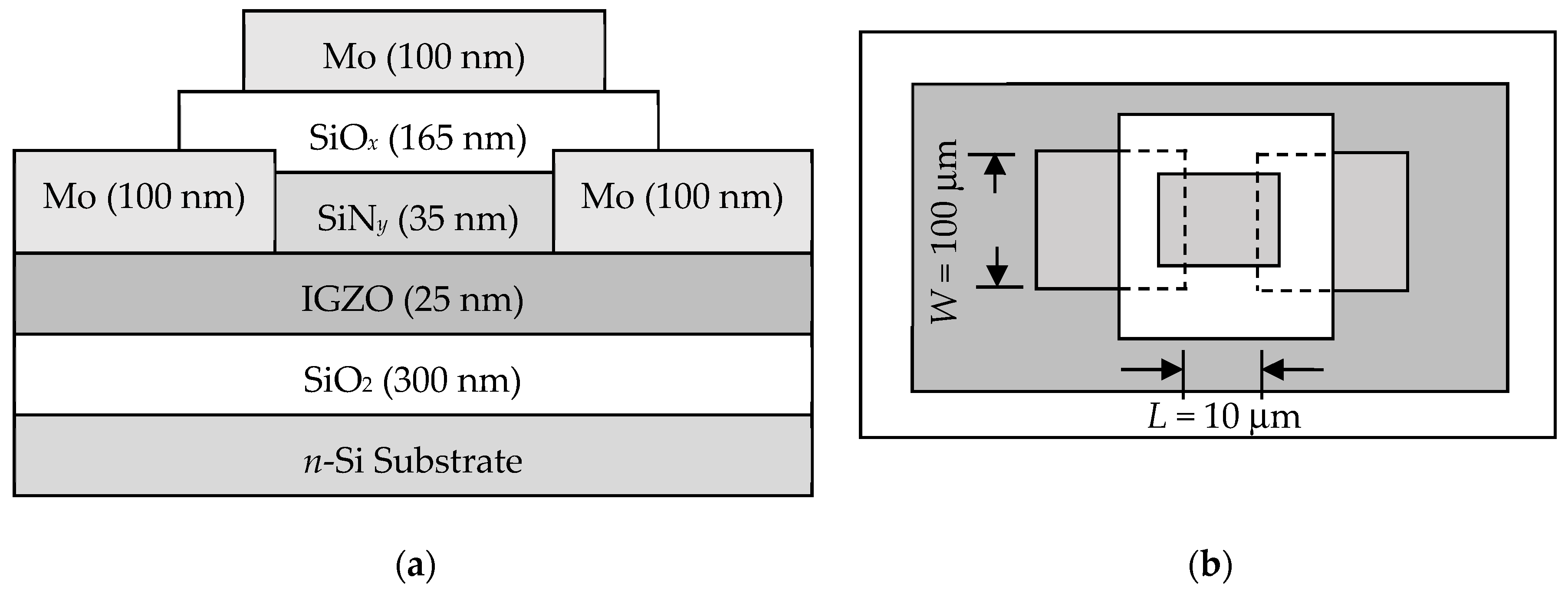
In the TFT samples prepared by this study, the gate dielectric material was a stack of SiO
x and SiN
y with the dielectric constants of 3.9 and 7.5 [
19], respectively. For subsequent calculations of transfer characteristics of
a-IGZO TFTs, we fabricated MIM samples with Mo/SiO
x/SiN
y/Mo structure and measured their capacitance-versus-voltage (
C-
V) profiles at 1 MHz. As shown in
Figure 8, one can see that the total capacitances of as-deposited and 300 °C-annealed samples are nearly the same.
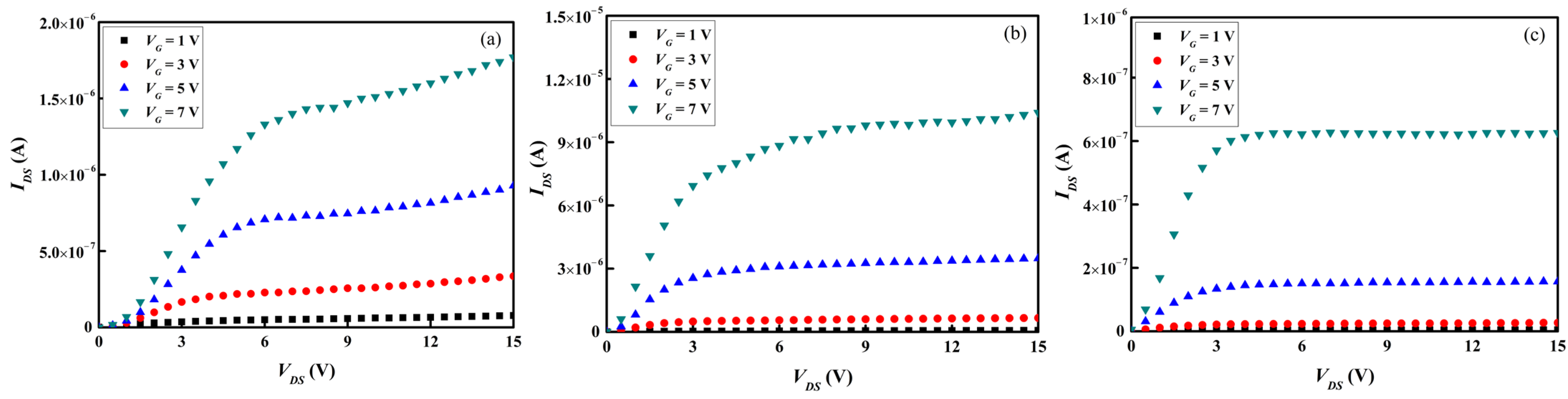
Figure 9a–c and
Figure 10a–c present separately the transfer and output characteristics of the TFT samples containing the three types of as-deposited
a-IGZO active channel layers. The transfer characteristics, i.e.,
Vth,
μFE,
SS, and
Ion/
Ioff, were calculated in accordance with the data presented in
Figure 9a–c, and the results are summarized in
Table 4. The
Vth’s of all the TFTs are about 2 V, indicating that a positive voltage is required for carrier extraction. Although the performance of TFT containing an
a-InGaZnO
4 channel layer is the best among the three types of TFT samples, its
μFE is only 1.65 cm
2·V
−1·sec
−1, as shown in
Table 4. A previous
C-V study performed in our laboratory [
11] demonstrated a rather rapid shift from depletion region to accumulation region in annealed samples, and a reduction in trap density at an
a-IGZO/SiO
2 interface for about one order of magnitude was observed. This implied that a post-annealing at 300 °C for 1 h in an ambient atmosphere may lead to a well-formed
a-IGZO/SiO
2 interface in the TFT sample. This study hence carried out the annealing of a gate dielectric layer and the post-annealing of TFT samples to improve the device performance. The annealing of the gate dielectric layer was intended to modulate the Mo/IGZO interface and suppress the defects at the SiO
x/SiN
y/Mo interface, and the post-annealing was intended to eliminate the water and oxygen adsorption in the ambient atmosphere during the device fabrication and reduce the interfacial defects between the layers of TFTs [
20,
21].
Figure 11a–c and
Figure 12a–c present separately the transfer and output characteristics of the three types of
a-IGZO TFT devices subjected to the gate dielectric annealing at 300 °C for 1 h in an ambient atmosphere. As listed in
Table 5, which summarizes the transfer characteristics of such TFT samples, one can see that the device performance is improved. Compared to the TFT samples containing as-deposited
a-IGZO channel layers,
Vth shifts toward the negative bias and both
SS,
μFE, and
Ion/
Ioff are improved.
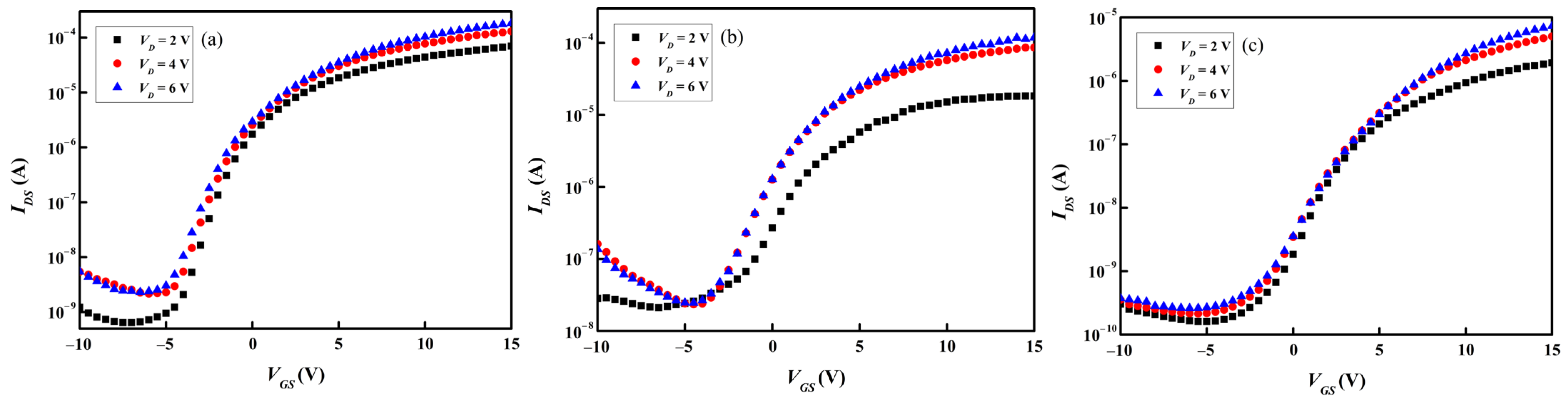
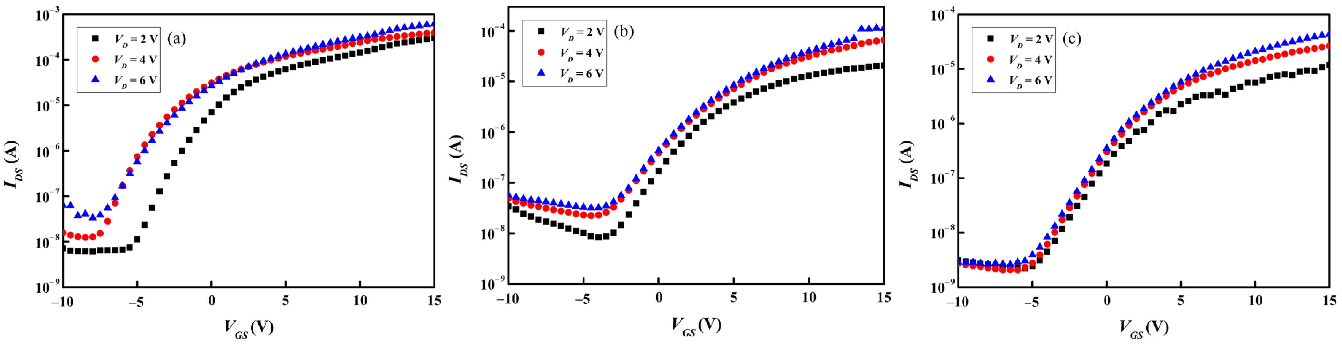
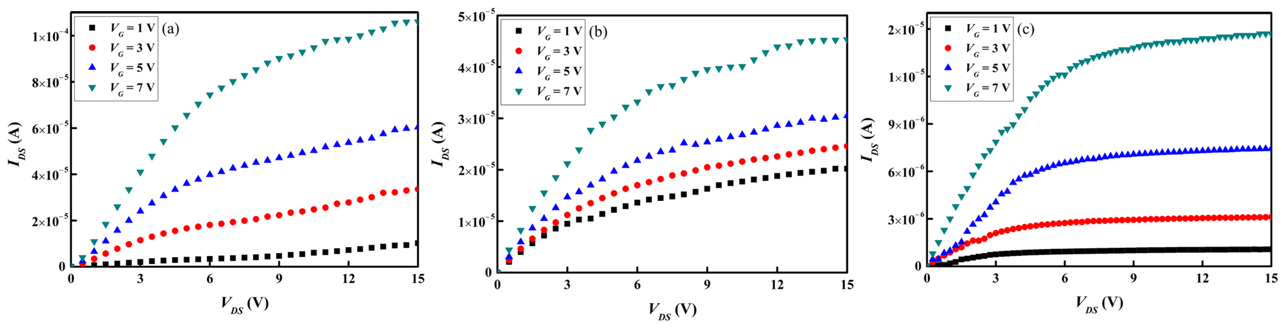
Figure 13a–c and
Figure 14a–c present separately the transfer and output characteristics of the three types of
a-IGZO TFT devices subjected to post-annealing at 300 °C for 1 h in an ambient atmosphere. The transfer characteristics listed in
Table 6 show that the
Vth further shifts toward the negative bias and that the
μFE is significantly improved. The
a-InGaZn
2O
5 TFT device exhibits the highest
μFE of 9.95 cm
2·V
−1·sec
−1, whereas the
μFE of the
a-InGa
2ZnO
5.5 TFT device is the lowest of 1.97 cm
2·V
−1·sec
−1. This is possibly ascribable to the difference in Ga content in the
a-IGZO channel layer of the TFT samples, which affects the mobility property of the
a-IGZO layers, as stated in the previous section. Overall, the best performance was observed in the
a-InGaZnO
4 TFT sample subjected to the 300 °C-post annealing with
Vth = −0.85 V,
μFE = 8.46 cm
2·V
−1·sec
−1,
SS = 2.31 V·decade
−1, and
Ion/
Ioff = 2.9 × 10
4.
InGaZnO
4 is the most popular type of active channel layer for
a-IGZO TFT devices, and the transfer characteristics of such devices reported by previous studies are listed in
Table 7. Compared with the TFT performance presented in
Table 7, the
a-InGaZnO
4 TFT device in this study should have achieved a satisfactory
μFE property, whereas a further refinement in device structure is required to improve the
Ion/
Ioff value. As to the TFT devices containing other types of
a-IGZO layers, Lee et al. [
1] prepared an
a-In
2Ga
2ZnO
7 layer for the TFT devices and obtained an
μFE of 4.2 ± 0.4 cm
2·V
−1·sec
−1 and an
SS of 0.96 ± 0.10 V·decade
−1. This is inferior to the
a-InGaZnO
4 TFT performance as listed in
Table 7, implying the high Ga content of the
a-IGZO channel layer might deteriorate the
μFE and
SS properties of the TFT devices. Shin et al. [
4] deposited the
a-IGZO layers at various oxygen ratios and their composition analysis found the Ga content of the
a-IGZO layers increases with the oxygen ratio. Due to the tight attraction of the Ga
3+ ions to the oxygen ions, which consequently reduces the number of charge carriers generated by the oxygen vacancies, Shin et al. observed a decrement in the
μsat and
SS values of the TFT devices when the Ga content of the
a-IGZO layer increases [
4]. As illustrated by the transfer characteristics of
a-IGZO TFT devices listed in
Table 6, similar effects of Ga content on TFT performance were also observed in this study. The incorporation of Ga in
a-IGZO channel layers might avoid the TFT devices in normally-on state; however,
a-IGZO channel layers with appropriate Ga contents are essential to accomplish TFT devices with satisfactory electrical properties.


