Article

Realizing Efficient Photoelectrochemical Performance for Well-Designed CdS@ZnIn2S4 Heterostructure Photoanode with Directional Interfacial Charge Transfer Dynamics

1
Micro-Electronics Research Institute and School of Electronics and Information, Hangzhou Dianzi University, Hangzhou 310018, China
2
National Laboratory of Solid State Microstructures, Department of Physics, Nanjing University, Nanjing 210093, China
*
Authors to whom correspondence should be addressed.
Coatings 2022, 12(8), 1210; https://doi.org/10.3390/coatings12081210
Submission received: 18 July 2022 / Revised: 14 August 2022 / Accepted: 16 August 2022 / Published: 18 August 2022
(This article belongs to the Special Issue Optical Thin Film and Photovoltaic (PV) Related Technologies)

Abstract

:
Designing a heterostructure photoanode with an appropriate band alignment, a beneficial charge migration pathway, and an adequate interfacial coupling is crucial for photoelectrochemical (PEC) energy conversion. Herein, we fabricate a hetero-nanostructure photoanode with CdS nanorods (CdS NRs) and two-dimensional (2D) ZnIn2S4 nanosheets (ZIS NSs) via a two-step in situ growth method on FTO glass to acquire a sufficient interfacial contact between two semiconductors. Based on their electronic band structures, the CdS is designed to be firstly grown on FTO to act as a photoelectron transport layer and 2D ZIS is further fabricated on the CdS as a photohole accumulation layer to directly contact the electrolyte. Benefitting from the Type II band alignment between the CdS and ZIS, such a heterostructure significantly enhances the separation efficiency and prolongs the lifetime of photocarriers. More importantly, it ensures that photoholes accumulate on the 2D ZIS with a highly exposed surface area for an oxidation reaction at the surface-active sites, while the photoelectrons transfer to counter electrode for hydrogen evolution. The optimum CdS@ZIS heterostructure photoanode exhibits a superior PEC performance with a photocurrent of 4.19 mA/cm2 at 1.23 VRHE (two times that of the CdS and eight times that of ZIS) and an applied bias photo-to-current efficiency (ABPE) of 1.93% at 0.49 VRHE. This work can inspire the future design of heterostructure photoanodes for highly efficient solar energy conversion.

1. Introduction

With the rapid development of technology and the economy, environmental pollution and the depletion of fossil resources are becoming increasingly serious [1]. The discovery of clean and environmentally friendly alternative energy resources has become a top priority for societies worldwide [2]. Solar energy is considered to be an ideal renewable energy due to its cleanness, environmental friendliness, and its abundant reserves [3]. However, the discontinuous and unstable capture of daylight greatly increases the difficulty in making full use of light resources, and the high cost of energy storage makes it challenging to popularize and utilize solar energy [4]. Photoelectrochemical (PEC) water splitting has provoked widespread attention as a promising approach to producing hydrogen via sunlight ever since Fujishima and Honda successfully decomposed water using a TiO2 electrode in 1972 [5]. By simulating the basic physical processes of natural photosynthesis, PEC technology converts photon energy into chemical energy, which accomplishes the effective conversion and storage of low-density solar energy [4,6].
Semiconductor photoanodes with an appropriate bandgap and band edge position play an essential role during the PEC conversion process. A large number of semiconductors, including ZnO [7,8,9], TiO2 [10,11], BiVO4 [12,13], and α-Fe2O3 [6,14,15], have been studied for PEC applications in the past decades. However, it is difficult for a single perfectly crystalized semiconductor to realize a superior PEC performance owing to its ultrahigh recombination rate of photoinduced electron-hole pairs [7]. In order to overcome such a drawback, numerous efforts have recently been attempted that involve constructing a heterostructure, introducing vacancies at the surface of the photoanode, and establishing nanocomposites with metal nanoparticles [16,17,18,19]. Among these strategies, the construction of a heterostructure between two suitable semiconductor materials is regarded as a promising method to handle the issue. An appropriate electronic structure difference between two semiconductors can not only merely optimize the optoelectronic of the heterostructure system, but more importantly, it can enhance the charge separation efficiency and prolong the lifetime of photocarriers [6]. There are various studies on building heterostructures to improve PEC performance. Ho et al. increased the saturation photocurrent by 46% via forming CdS/MoS2 core/sheath heterojunction nanostructures [20]. Xu et al. reported a type of FeBi/BiVO4 heterostructure exhibiting a sevenfold improvement in its photocurrent density compared with pure BiVO4 [21]. Hu et al. synthesized TiO2@ZnO core shell structures that realized an effective interfacial charge separation and obtained a conversion efficiency that was 2.7 times higher than pristine TiO2 nanorods arrays [22].
Most reported works about the construction of heterostructures have mainly focused on finding semiconductors with an appropriate energy band alignment for realizing an enhanced charge separation near the heterointerface [13,22,23]. Besides matched electronic structures, the precise control of the migration pathway of negatively charged photoelectrons and positively charged photoholes, as well as the adequate interfacial coupling between two semiconductors, also play essential roles in improving the solar light conversion efficiency of photoanodes [19]. Thus, the simultaneous integration of the aforementioned three elements in a heterostructure system through a deliberate microstructure design can be expected to achieve an advantageous PEC performance [24]. Herein, we select CdS nanorods (CdS NRs) with a superior photoexcitation efficiency and two-dimensional (2D) ZnIn2S4 nanosheets (ZIS NSs) with a large surface area to construct a hetero-nanostructure with a Type-II energy band alignment. A two-step in situ growth method on fluorine-doped tin oxide (FTO) glass has been adopted to acquire a sufficient hetero-interface contact between CdS NRs and ZIS NSs. Considering the higher valence band maximum (VBM) and conduction band minimum (CBM) of ZIS compared to CdS, it can be expected that the photoelectrons of ZIS will transfer to the CBM of the CdS NRs and the photoinduced holes of CdS will accumulate on the 2D ZIS under irradiation. Therefore, the CdS NRs are deliberately designed to be firstly grown on FTO to act as a photoelectron transport layer, and the 2D ZIS is further fabricated on CdS NRs as a photohole accumulation layer to directly contact the electrolyte. Such a well-designed heterostructure can considerably improve the separation efficiency and prolong the lifetime of photoinduced carriers. More importantly, it ensures that photoholes are enriched on the 2D ZIS with a highly exposed surface area to participate in oxidation reactions at the surface-active sites, while the photoelectrons are transferred to the counter electrode through the external circuit. Such favorable interfacial charge transfer dynamics are highly beneficial for the enhancement of the PEC conversion efficiency. The photocurrent density of the optimum CdS@ZIS heterostructure photoanode reaches 4.19 mA/cm2, which is twice that of a single CdS NR and eight times that of ZIS NSs. The applied bias photo-to-current efficiency (ABPE) of the CdS@ZIS photoanode achieves a high value of 1.93% at 0.49 V vs. the RHE.

2. Materials and Methods

2.1. Materials

All reagents involving Cadmium nitrate tetrahydrate (CdN2O6·4H2O), Indium (III) chloride tetrahydrate (InCl3·4H2O), Zinc chloride (ZnCl2), thiourea (CH4N2S), and reduced L-Glutathione (C10H17N3O6S) were purchased from Shanghai Macklin Biochemical Co., Ltd. and have all been used directly without any purification. We have listed the details of the chemicals used in the experiments in Table 1.

2.2. Photoanode Preparation

2.2.1. Preparation of CdS Nanorods

The CdS NRs were grown on FTO glass substrate using an in situ hydrothermal method. First, FTO substrates were cleaned with acetone, ethanol, and deionized water for ten minutes each in ultrasonic cleaner. Meanwhile, 149.5 mg Cd(NO3)2·4H2O, 90.3 mg glutathione, and 36.9 mg thiourea were added into 10 mL deionized water and mixed well under magnetic stirring at room temperature for a few minutes. Then, the solution was transferred to a 25-mL Teflon-lined autoclave with clean FTO substrates, which were vertically placed on a custom mold to conduct the solvothermal reaction at 200 °C for 2 h. After the reaction was completed and the solution had cooled to room temperature, the yellow-colored nanorods grown on FTO were obtained and washed with ethanol and deionized water three times to remove impurities from its surface.

2.2.2. Preparation of CdS@ZIS

The CdS@ZIS heterostructure was prepared by an improved solvothermal method. First, 7 mg ZnCl2, 29.3 mg InCl3·4H2O, and 30.4mg thiourea were dissolved in a mixed solution of 9 mL deionized water and 9 mL ethanol. After thorough stirring, the solution was transferred to a 25-mL Teflon-lined autoclave containing the as-prepared CdS photoanode leaning against the wall with its conductive side facing down, and the hydrothermal reaction was conducted at 170 °C for 6 h. Finally, The CdS@ZIS photoanode was washed several times with deionized water and ethanol after cooling to room temperature and then dried in the air for a period of time. To further change the thickness of ZIS NSs, the concentration ratio of precursors was adjusted to 1:0.5:0.2. Below, for the convenience of expression, we abbreviated the three concentrations as HC (original concentration or high concentration, 1:1), MC (medium concentration, 1:0.5), and LC (low concentration, 1:0.2), respectively.

2.3. Characterization

2.3.1. Standard Characterization

The crystalline structures and phase compositions of all samples were characterized by X-ray diffractometer (XRD, MiniFlex600, Rigaku, Tokyo, Japan). The morphology and elemental compositions were identified by field-emission-scanning electron microscope (FESEM, SU-1510, HITACHI, Tokyo, Japan) equipped with an energy dispersive X-ray spectrometer (EDS). Ultraviolet—visible (UV—vis) diffuse reflectance spectra were determined by UV—vis spectrophotometry (U-2550, HITACHI, Tokyo, Japan) with an integrating sphere over a wavelength range from 300 to 600 nm (BaSO4 as the reference).

2.3.2. Photoelectrochemical Characterization

The electrochemical and PEC performances were carried out with a three-electrode system in 0.5 M Na2SO4 and 0.5 M Na2SO3 aqueous solution using CHI-660E electrochemical workstation. Typically, the prepared photoanode, Pt net, and Ag/AgCl were used as the working electrode, counter electrode, and reference electrode, respectively. A 300 W Xe-lamp coupled with an AM 1.5G filter served as simulated sunlight and the working electrode was illuminated from the back side. All measured potentials (V vs. Ag/AgCl) were converted to reversible hydrogen electrode (RHE) using Equation (1) [6]:
ERHE = EAg/AgCl + EAg/AgCl(reference) + 0.0591 V × pH
where ERHE = EAg/AgCl(reference) equals 0.1976 V at 25 °C. Incident photon-to-current efficiency (IPCE) was examined at 1.23 V (vs. RHE) under monochromatic light obtained by filters with specific wavelength. Electrochemical impedance spectroscopy (EIS) was measured at a frequency range of 0.1 Hz to 100 kHz with an amplitude of 5 mV without illumination. Mott–Schottky plots were obtained at a frequency of 500 Hz with AC amplitude of 5 mV in the dark.

3. Results and Discussion

3.1. Design and Construction of CdS@ZIS Heterostructure

A well-designed two-step in situ solvothermal method was adopted to fabricate the CdS@ZIS heterostructure photoanode and the concentration of ZIS precursor was deliberately modulated, as displayed in Figure 1. At first, the CdS NRs were perpendicularly grown on FTO using Cd(NO3)2·4H2O, thiourea, and glutathione as precursors. It should be noted that the capping agent, glutathione, in an appropriate concentration plays a vital role in the formation of CdS nanorods. An excessive concentration of glutathione would result in the spherical structure of the CdS and create a barrier between the photoanode and the electrolyte, which would adversely affect the carrier transfer [25,26]. It is obvious that such a nanorod-array structure can not only provide a more abundant surface area for contact with ZIS NSs, but also significantly enhance the photo absorption via multilevel reflection and the scattering of solar light [6,27]. Moreover, a nanorod morphology can provide the CdS with an electron transport pathway along its axial direction, which is favorable for the separation of photoinduced electron—hole pairs [28]. As shown in Step II, the ZIS with a 2D nanosheet morphology further directly crystallizes on the CdS nanorod array via the in situ solvothermal method [28,29]. The large specific surface area of 2D ZIS NSs can provide abundant surface-active sites to interact with reactive species in the electrolyte, which is beneficial to the surface oxidation reaction rate [29]. Meanwhile, the two-dimensional structure can provide a shorter diffusion distance to effectively inhibit the photocarrier recombination before reaching the surface. More importantly, the 2D structure feature provides the ZIS more chances to realize effective interfacial electronic coupling with the CdS NRs [3,28]. To optimize the microstructure of the CdS@ZIS photoanode, the concentration of ZIS precursor was regulated. A variation in the precursor concentration results in the formation of different numbers of nucleation centers, which affects the growth rate of ZIS [28,30]; therefore, a high concentration (HC) of precursor will lead to an ultrathick ZIS layer. The excessive ZIS NSs without a direct interfacial contact with the CdS NRs not only do not contribute to charge separation but are also averse to the photohole transfer to the surface for conducting oxidation reactions. In addition, the overload of the ZIS will induce a light-shielding effect. Therefore, the construction and precise microstructural control of the CdS@ZIS hetero-nanostructure can be expected to play vital roles on the charge dynamics and PEC performance.

3.2. Microstructure and Composition Characterization

The FESEM images of the CdS NRs and the CdS@ZIS (LC) photoanodes are shown in Figure 2a,b to further explore the morphology of the CdS NRs and the CdS@ZIS photoanodes. As displayed in Figure 2a, CdS grown on an FTO substrate has a hexagonal rod-like structure in accordance with previous reports [20,27]. From the top-view image, we can clearly observe that the CdS NRs photoanode has a uniform and vertically aligned nanorod-array structure and the average diameter of the nanorods is approximately 200 nm. Furthermore, the gaps among the nanorods provide the insertion space for the 2D ZIS NSs to form a sufficient interfacial contact between the two semiconductors and are beneficial to the enhanced photo absorption via the multilevel reflection and scattering of incident light. As shown in Figure 2b, the 2D ZIS NSs with uniform dimension and shape prepared via an in situ hydrothermal method are accumulated on the topside of the CdS nanorods arrays as expected. For comparison, the FESEM image of the CdS@ZIS (HC) is displayed in Figure S1. It is evident that a high concentration of the ZIS precursor results in a thicker ZIS layer, which is consistent with our previous expectation.
To determine the elemental composition of the CdS@ZIS heterostructure, energy dispersive spectrometry (EDS) was carried out and is exhibited in Figure 2c. The presence of Cd, Zn, and In elements indicates that the ZIS was successfully grafted onto the CdS. As for the Sn element, it comes from the FTO glass, which was used as a conductive substrate. XRD patterns were determined to confirm the phase and crystal structures of the as-prepared photoanode, as displayed in Figure 2d. In addition to the peaks of the FTO, all the other diffraction peaks of the nanorod array at 26.35°, 29.76°, 38.10°, 45.18°, and 49.27° are indexed to the (100), (101), (102), (110), and (103) facet of the CdS with a hexagonal wurtzite crystal structure (JCPDS no. 41-1049) [20]. In comparison to the pristine CdS NRs, the XRD pattern of the CdS@ZIS displays additional peaks located at 22.67°, 28.97°, 48.59°, and 57.36°, corresponding to the (006), (102), (110), and (203) crystal planes of the hexagonal phase ZIS (JCPDS no. 65-2023), respectively [31]. It should be noted that these diffraction peaks belonging to the ZIS NSs have a relatively weak diffraction intensity compared to the CdS NRs, which agree well with the ultrathin nanosheet structure of ZIS as well as the lower concentration of ZIS precursors (for comparison, the XRD pattern of ZIS (HC) is displayed in Figure S2). The above results indicate that the pure CdS@ZIS heterostructure with an adequate interfacial contact were successfully synthesized as designed.

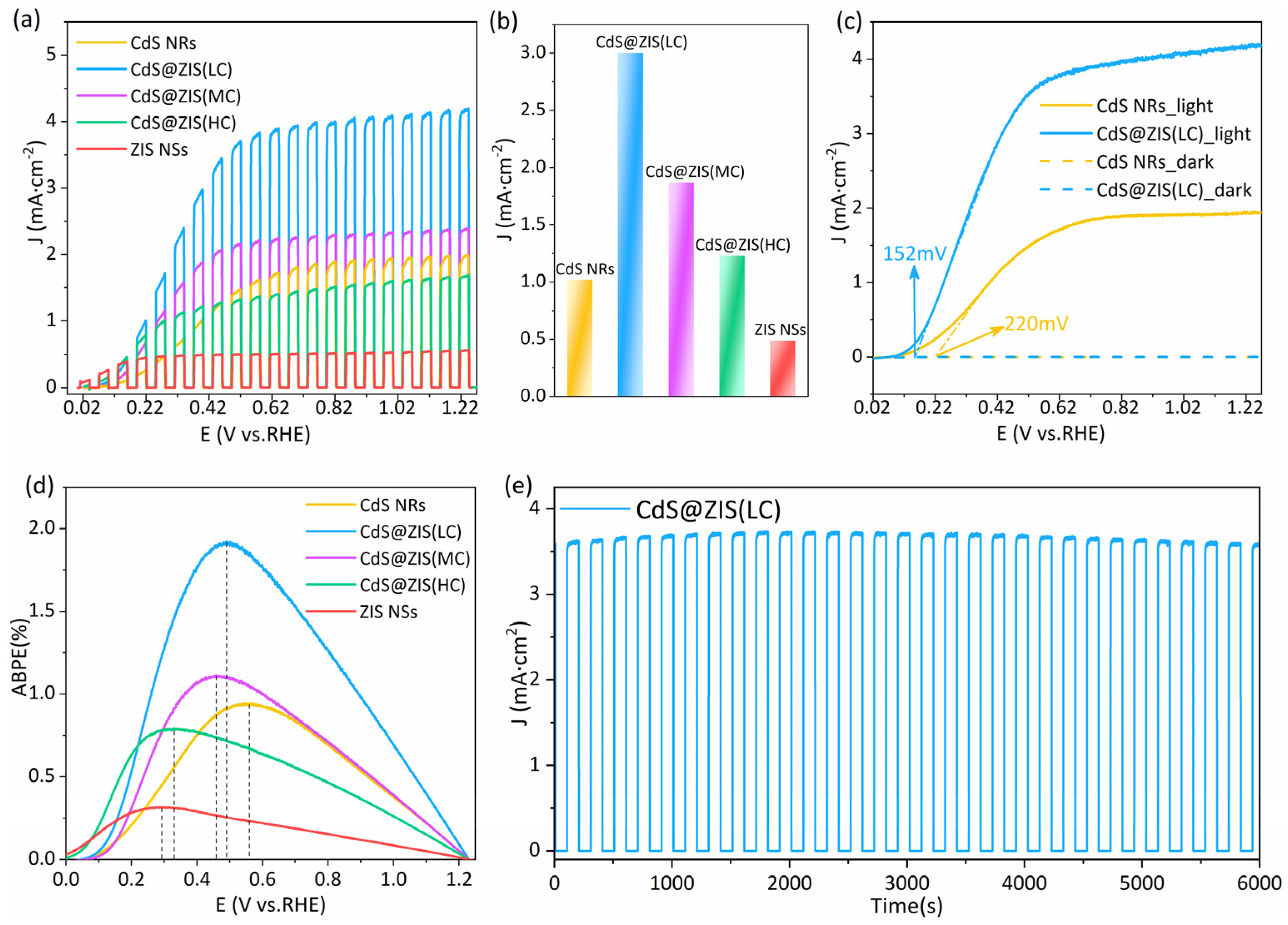
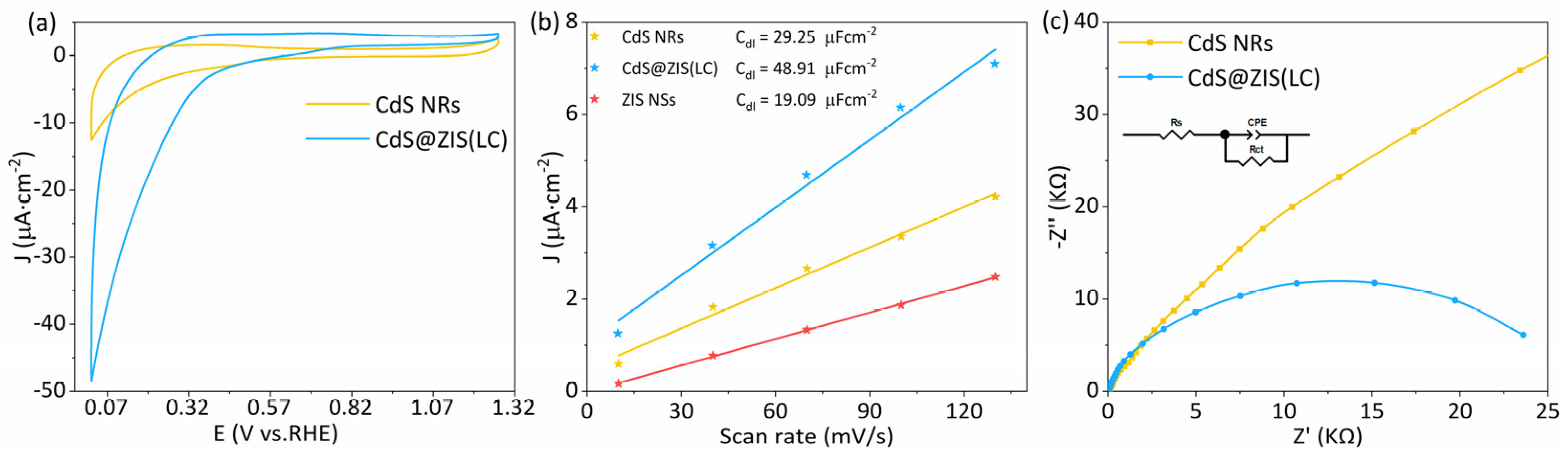
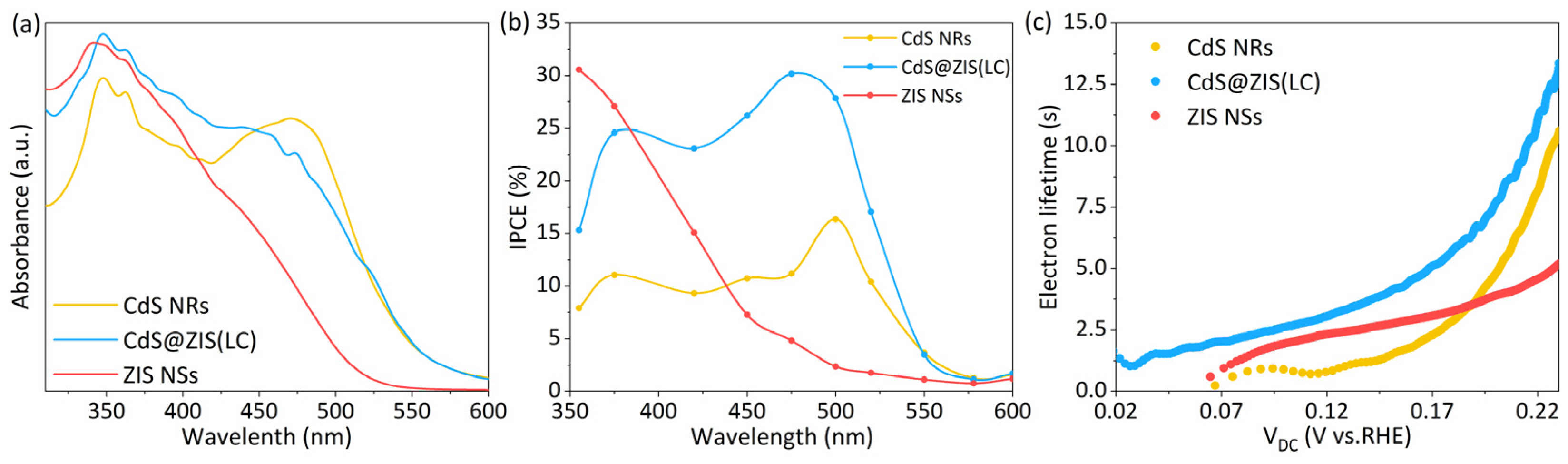
3.3. Photoelectrochemical Performance and Electrochemical Analysis

The PEC measurements were conducted in a traditional three-electrode system. Linear sweep voltammetry (LSV) curves under chopped irradiation are shown in Figure 3a. Limited by its high photocarrier-recombination rate, the CdS NRs photoanode with the ideal photoexcitation efficiency merely exhibits photocurrent density of 1.97 mA/cm2 at 1.23 V vs. RHE. Whereas the three kinds of the CdS@ZIS heterostructure photoanodes with different loading amounts of ZIS all achieve evidently enhanced photocurrent densities. The optimal CdS@ZIS reaches 4.19 mA/cm2 at 1.23 V vs. RHE, reaching two times that of pure CdS and eight times that of pure ZIS. Notably, the optimal heterostructure photoanode is the CdS@ZIS (LC) instead of the CdS@ZIS (HC), which indicates that such an evidently enhanced PEC performance was mainly contributed by the interfacial electronic coupling between the CdS NRs and ZIS NSs rather than the simple integration of their optoelectronic properties [16]. To further reveal the effect of the concentration of ZIS precursors on the PEC performance of the CdS@ZIS heterostructure photoanode, the photocurrent density at 0.4 V vs. the RHE of the bare CdS NRs, CdS@ZIS (LC), CdS@ZIS (MC), and CdS@ZIS (HC) is displayed in Figure 3b. The photocurrent density exhibits a typical volcano plot along with the loading amount of ZIS NSs, which further corroborates that the highly enhanced PEC conversion efficiency of such a heterostructure photoanode is mainly due to the beneficial interfacial charge dynamics. Along with the further increment of the ZIS loading amount, the photocurrent density decreased, which resulted from the excessive nanosheets without direct contact with the CdS NRs interfering with their photohole migration to the surface-active sites of the ZIS [32,33]. The LSV curves are exhibited in Figure 3c to demonstrate the onset potential. The negligible dark current indicates that the photoanodes have a large charge transfer resistance in the dark. The onset potential of the CdS@ZIS (LC) (152 mV) exhibits a negative shift of 68 mV compared to the pristine CdS NRs (220 mV), indicating the highly promoted photovoltage after constructing the heterostructure with ZIS NSs. The applied bias photon-to-current efficiency (ABPE) values were investigated to obtain the solar conversion efficiency of the photoanode, as shown in Figure 3d. Based on the LSV curves under the simulated solar light in Figure S3, the ABPE values are calculated by Equation (2) [33].
ABPE (%) = [J × (1.23 − Vb)]/PTotal,
where J is the measured photocurrent density, Vb is the applied bias vs. the RHE, and PTotal is the total intensity of incident light (135 mW/cm2). The CdS@ZIS (LC) achieves the maximum ABPE value of 1.91% at 0.49 V vs. the RHE, which is much higher than the CdS NRs (0.94% at 0.56 V vs. RHE) and ZIS NSs (0.31% at 0.29 V vs. RHE). Furthermore, the potential corresponding to the maximum photoconversion efficiency shows an evident negative shift with an increasing ZIS precursor concentration, which reveals that the introduction of ZIS NSs evidently enhances the separation efficiency of the photogenerated carriers under a low bias and leads to a higher photovoltage to drive the surface redox reaction. The stability of the CdS@ZIS (LC) was determined at 1.23 V vs. the RHE under a continuous 100 min illumination. As shown in Figure 3e, the photocurrent density has remained stable without a significant attenuation, which can be attributed to the heterostructure construction that facilitates the photogenerated holes’ transfer to the ZIS NSs and that alleviates the photo corrosion of the CdS NRs.
Cyclic voltammogram (CV) analyses of the CdS NRs and CdS@ZIS (LC) were conducted at a fixed scan rate of 50 mV/s to characterize the electrochemical activity and charge storage capacity, as exhibited in Figure 4a [34]. The improved dark current of the CdS@ZIS (LC) in contrast to the CdS NRs demonstrates that the introduction of 2D ZIS NSs with a large surface area provides many more active sites for surface redox reactions [34]. Moreover, the CdS@ZIS (LC) exhibits a larger voltammogram area than that of the CdS NRs, which suggests that the heterostructure shows a larger capacitance and can store and release higher concentrations of electrons [32,35]. To further evaluate the electrochemically active surface area (ECSA) of the obtained photoanodes, the electric double layer capacitance (Cdl) was calculated using the variable scan rate of the CV in Figure S4. The ECSA is calculated via Equation (3) [36].
ECSA = Double layer capacitance (Cdl)/Cs,
where Cs is the specific capacitance of a flat surface. As observed from Figure 4b, compared with the CdS NRs, the tendency of the Cdl of the CdS@ZIS achieves great improvements, indicating that the ZIS NSs growing on the CdS NRs provide enough of a specific surface area and expose more active sites for the redox reaction occurring on the interface between the photoanode and electrolyte [34]. EIS was carried out to reveal the conductivity and charge transfer resistance at the electrode/electrolyte interface. The EIS was obtained by the Nyquist plot in Figure 4c and modelled according to the equivalent circuit in the inset, where Rs, Rct, and CPE are the electrolyte solution resistance, the charge transfer resistance, and the constant phase element, respectively [13]. It is worth mentioning that the CPE is utilized in the equivalent circuit to fit the impedance data rather than the capacitance owing to the ability of the CPE to reveal the possible interface states caused by defects or impurities [16]. The Nyquist curve radius characterizing the interface transfer impedance of the CdS@ZIS (LC) is smaller than that of the pure CdS NRs, which is beneficial to the photocarrier migration and inhibits the recombination of photoinduced electron-hole pairs. Furthermore, the Rct values estimated from impedance spectrum and equivalent circuit are 103.0 kΩ and 26.8 kΩ for CdS NRs and CdS@ZIS (LC), respectively, which further proves that the heterostructure construction effectively improves the separation efficiency of photoexcited carriers and reduces the charge transfer resistance at the interface of the photoelectrode and electrolyte. Such a sharply decreased charge transfer resistance benifits from the highly exposed surface area of the 2D ZIS as well as the efficient interfacial electronic coupling between the CdS NRs and ZIS NSs.
The optoelectronic property of the photoanode is one of the most important factors of PEC performance. The UV–vis diffusive reflectance spectra are explored to determine the photo absorption properties, as shown in Figure 5a. Evidently, the CdS shows a wider photo absorption range with a cut-off wavelength of 560 nm compared to the ZIS’s 510 nm. Thus, the introduction of the ZIS NSs onto the CdS NRs will not broaden the light absorption range. While benefiting from electronic structure of ZIS, the absorbance of the heterostructure exhibits a certain enhancement from 310 nm to 425 nm. The incident photon-to-current efficiency (IPCE) was tested to verify the contribution of monochromatic light with different photon energies to the photocurrent density and calculated via Equation (4) [27].
IPCE (%) = (1240 × Jλ)/(λ × Pλ) × 100,
where λ is wavelength of incident light, and Jλ and Pλ are the corresponding photocurrent density and power density. As shown in Figure 5b, the IPCE of the CdS@ZIS (LC) is much larger than the pure CdS and ZIS from the 400 nm to 550 nm. After the CdS NRs formed a heterostructure with the ZIS NSs, the IPCE at 480 nm reached 31%, which is almost threefold that of the CdS photoanode (11%). In fact, the ZIS photoanode exhibits a quite low IPCE value at wavelengths larger than 480 nm owing to the negligible photo absorption for the photon energy smaller than the forbidden gap. Thus, the evident improvement of the IPCE at wavelengths from 450 nm to 550 nm compared with the pure CdS does not originate from the enhanced photon absorption and increased photocarrier generation rate but was caused by the highly promoted photocarrier separation efficiency through beneficial interfacial charge dynamics between CdS and ZIS. The transient open-circuit potential (Voc) was determined to analyze the dynamics of the non-balanced photocarrier (Figure S5). The negative shift of the Voc under light irradiation agrees well with the electronic properties of n-type semiconductors [6]. Based on the curves of the Voc evolving with time, the electron lifetime (τ) can be calculated by Equation (5) [6].
τ = −kbT/e × (dVoc/dt)−1,
where kb is the Boltzmann constant, T is the temperature, and e is the elementary electric charge. As exhibited in Figure 5c, it is evident that the CdS@ZIS (LC) exhibits an elongated electron lifetime compared with the pristine CdS NRs and ZIS NSs, which demonstrates that constructing such a heterostructure effectively inhibits the intrinsic recombination of the photogenerated carriers, thus prolonging the lifetime of the photocarriers and creating more opportunities for them to diffuse to the surface-active sites to conduct energy-conversion reactions.

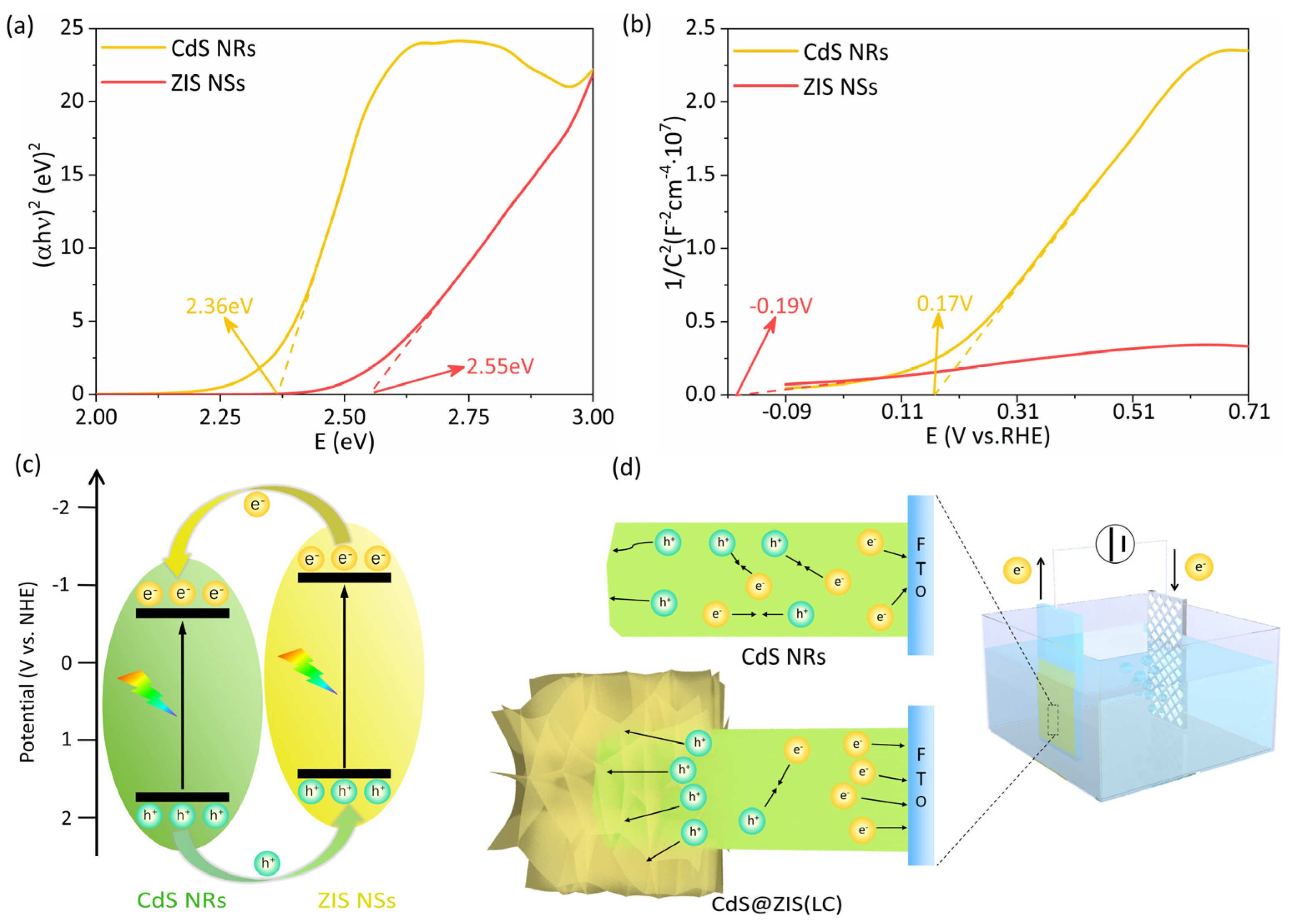
3.4. Highly Beneficial Photoinduced Charge Dynamics via Rational Microstructure Design

In order to comprehensively reveal the mechanism behind the highly improved PEC performance of the CdS@ZIS heterostructure photoanode, the electronic band structures of both semiconductors must be determined. To estimate their bandgap, Tauc plots of the CdS NRs and ZIS NSs were converted based on the UV—vis spectrum in Figure 5a. As shown in Figure 6a, the calculated optical bandgaps of the pure CdS and ZIS are 2.36 eV and 2.55 eV, respectively. The flat-band potential (Efb) was measured from the x-intercept of a linear fit to the Mott–Schottky plots to determine the relative positions of the conduction band (CB) of the two semiconductors. A Mott–Schottky measurement was carried out at a frequency of 500 Hz in dark conditions, as displayed in Figure 6b. It is obvious that the Efb (vs. RHE) of the CdS is more positive than that of ZIS, which can reflect the relative position of the CB level, and the CB position of the ZIS is about 0.35 eV more negative than the CdS.
Combining the above analysis results with the CB position of the CdS NRs reported in previous research (−0.70 V vs. NHE) [3], the staggered energy band alignment inducing a Type-II charge transfer pathway between the CdS NRs and ZIS NSs was formed, as shown in Figure 6c, and a possible mechanism whereby the heterostructure regulates the directional migration of the photogenerated electron-hole pairs is revealed in Figure 6d. Although the CdS NRs with a narrower bandgap can be easily excited by solar light to generate numerous photoinduced carriers, the strong Coulomb interactions between the photoinduced electrons and the holes of the CdS NRs as well as the lack of surface-active sites at the interface of the photoelectrode/electrolyte lead to the fast intrinsic recombination of the electron-hole pairs, resulting in fewer chances to participate in redox reactions. After introducing the 2D ZIS NSs with a larger specific surface area to construct the hetero-nanostructure with a matched energy band alignment, the photogenerated holes at the valence band (VB) of the CdS NRs spontaneously migrate to the VB of the ZIS NSs due to the more negative VB position of the ZIS (1.66 V vs. NHE for CdS and 1.49 V vs. NHE for ZIS), and then transfers to the photoanode/electrolyte interface to participate in the oxidation reaction. In the meantime, the photoinduced electrons located at the CB of the ZIS NSs can easily inject themselves into the CB of the CdS NRs and finally be transported to the Pt counter electrode via the FTO substrate and external circuits for the hydrogen evolution reaction. Therefore, the fabrication of ZIS NSs on the top side of the CdS NRs to form a Type II heterostructure not only merely induces the separation of photoexcited carriers near the hetero-interfaces, but also drives photoinduced holes and electrons to accumulate on the ZIS layer, which interacts with the electrolyte, and the CdS layer, which interacts with the FTO. Such a directional photocarrier transfer finally results in the superior PEC performance of the CdS@ZIS heterostructure photoanode.

4. Conclusions

In summary, we designed and fabricated an effective CdS NRs/2D ZIS NSs heterostructure via a two-step in situ growth method. A photoanode with an excellent PEC performance was obtained by changing the concentration of the ZIS precursor to regulate the loading amount of the ZIS NSs on the CdS NRs. The comprehensive characterization and analyzation demonstrated that the construction of such a Type II heterostructure—with an appropriate energy band alignment, a precise migration pathway, and an adequate interfacial coupling—can not only significantly improve the separation efficiency of photogenerated electron-hole pairs, but also ensure that the photoholes are enriched on the 2D ZIS with a highly exposed surface area to participate in oxidation reactions at the surface-active sites, while the photoelectrons are transferred to the counter electrode through the external circuit. The photocurrent density of the optimum CdS@ZIS photoanode achieved was 4.19 mA/cm2, which is twice that of bare CdS NRs and eight times that of ZIS NSs. The ABPE of the CdS@ZIS photoanode reaches a high value of 1.93% at 0.49 V vs. the RHE. This work provides a practical method for the construction of a high performance heterostructure for solar energy conversion applications.

Supplementary Materials

The following supporting information can be downloaded at: https://www.mdpi.com/article/10.3390/coatings12081210/s1, Figure S1. The FESEM images of CdS@ZIS (HC); Figure S2. XRD patterns of ZIS (HC); Figure S3. Photocurrent density versus potential curves of CdS NRs, ZIS NSs and CdS@ZIS with varied concentration of ZIS precursor; Figure S4. Cyclic voltammograms of (a) CdS NRs, (b) ZIS NSs and (c) CdS@ZIS(LC) at various scan rates from 10 to 130 mv/s; Figure S5. Transient open circuit potential plots under simulated solar light-switching.

Author Contributions

Conceptualization, X.W. and L.L.; methodology, X.W. and L.L.; investigation, X.W., Y.Q. and G.L.; resources, L.L., Y.Z. and D.W.; writing—original draft preparation, X.W.; writing—review and editing, X.W., L.L., Y.Z. and D.W.; supervision, L.L., Y.Z. and D.W.; funding acquisition, L.L., Y.Z. and D.W. All authors have read and agreed to the published version of the manuscript.

Funding

This work was supported by the NSF of China (Grant No. 12004089), National College Students Innovation and Entrepreneurship Training Program of China (Grant No. 202110336008), the Ten Thousand Talents Plan of Zhejiang Province of China (Grant No. 2019R52014), the Open Fund of Fujian Provincial Key Laboratory of Quantum Manipulation and New Energy Materials (Grant No. QMNEM2013), and the Fundamental Research Funds for the Provincial Universities of Zhejiang (Grant No. GK209907299001-012).

Institutional Review Board Statement

Not applicable.

Informed Consent Statement

Not applicable.

Data Availability Statement

The data presented in this study are available on request from the corresponding author.

Conflicts of Interest

The authors declare no conflict of interest.

References

  1. Braiek, Z.; Naceur, J.B.; Jrad, F.; Assaker, I.B.; Chtourou, R. Novel synthesis of graphene oxide/In2S3/TiO2 NRs heterojunction photoanode for enhanced photoelectrochemical (PEC) performance. Int. J. Hydrogen Energy 2022, 47, 3655–3666. [Google Scholar] [CrossRef]
  2. Wang, Y.; Wang, Q.; Zhan, X.; Wang, F.; Safdar, M.; He, J. Visible light driven type II heterostructures and their enhanced photocatalysis properties: A review. Nanoscale 2013, 5, 8326–8339. [Google Scholar] [CrossRef] [PubMed]
  3. Li, P.; Liu, M.; Li, J.; Guo, J.; Zhou, Q.; Zhao, X.; Wang, S.; Wang, L.; Wang, J.; Chen, Y. Atomic heterojunction-induced accelerated charge transfer for boosted photocatalytic hydrogen evolution over 1D CdS nanorod/2D ZnIn2S4 nanosheet composites. J. Colloid Interface Sci. 2021, 604, 500–507. [Google Scholar] [CrossRef] [PubMed]
  4. Yang, W.; Prabhakar, R.R.; Tan, J.; Tilley, S.D.; Moon, J. Strategies for enhancing the photocurrent, photovoltage, and stability of photoelectrodes for photoelectrochemical water splitting. Chem. Soc. Rev. 2019, 48, 4979–5015. [Google Scholar] [CrossRef]
  5. Fujishima, A.; Honda, K. Electrochemical photolysis of water at a semiconductor electrode. Nature 1972, 238, 37–38. [Google Scholar] [CrossRef]
  6. Long, L.; Lv, G.; Han, Q.; Wu, X.; Qian, Y.; Wang, D.; Zhou, Y.; Zou, Z. Achieving Direct Z-Scheme Charge Transfer through Constructing 2D/2D α-Fe2O3/CdS Heterostructure for Efficient Photocatalytic CO2 Conversion. J. Phys. Chem. C 2021, 125, 23142–23152. [Google Scholar] [CrossRef]
  7. Zhang, B.; Wang, Z.; Huang, B.; Zhang, X.; Qin, X.; Li, H.; Dai, Y.; Li, Y. Anisotropic photoelectrochemical (PEC) performances of ZnO single-crystalline photoanode: Effect of internal electrostatic fields on the separation of photogenerated charge carriers during PEC water splitting. Chem. Mater. 2016, 28, 6613–6620. [Google Scholar] [CrossRef]
  8. Gill, R.; Ghosh, S.; Sharma, A.; Kumar, D.; Nguyen, V.-H.; Vo, D.-V.N.; Pham, T.-D.; Kumar, P. Vertically aligned ZnO nanorods for photoelectrochemical water splitting application. Mater. Lett. 2020, 277, 128295. [Google Scholar] [CrossRef]
  9. Long, L.; Wu, Q.; Chao, Q.; Dong, Y.; Wu, L.; Zhang, Q.; Zhou, Y.; Wang, D. Surface-state-mediated interfacial charge dynamics between carbon dots and ZnO toward highly promoting photocatalytic activity. J. Chem. Phys. 2020, 153, 044708. [Google Scholar] [CrossRef]
  10. Wang, G.; Wang, H.; Ling, Y.; Tang, Y.; Yang, X.; Fitzmorris, R.C.; Wang, C.; Zhang, J.Z.; Li, Y. Hydrogen-treated TiO2 nanowire arrays for photoelectrochemical water splitting. Nano Lett. 2011, 11, 3026–3033. [Google Scholar] [CrossRef]
  11. Ai, G.; Li, H.; Liu, S.; Mo, R.; Zhong, J. Solar water splitting by TiO2/CdS/Co–Pi nanowire array photoanode enhanced with Co–Pi as hole transfer relay and CdS as light absorber. Adv. Funct. Mater. 2015, 25, 5706–5713. [Google Scholar] [CrossRef]
  12. Zhang, H.; Li, H.; Wang, Z.; Zheng, Z.; Wang, P.; Liu, Y.; Zhang, X.; Qin, X.; Dai, Y.; Huang, B. Fabrication of BiVO4 photoanode consisted of mesoporous nanoparticles with improved bulk charge separation efficiency. Appl. Catal. B Environ. 2018, 238, 586–591. [Google Scholar] [CrossRef]
  13. Bai, S.; Han, J.; Zhao, Y.; Chu, H.; Wei, S.; Sun, J.; Sun, L.; Luo, R.; Li, D.; Chen, A. rGO decorated BiVO4/Cu2O nn heterojunction photoanode for photoelectrochemical water splitting. Renew. Energy 2020, 148, 380–387. [Google Scholar] [CrossRef]
  14. Phuan, Y.W.; Ong, W.-J.; Chong, M.N.; Ocon, J.D. Prospects of electrochemically synthesized hematite photoanodes for photoelectrochemical water splitting: A review. J. Photochem. Photobiol. C 2017, 33, 54–82. [Google Scholar] [CrossRef]
  15. Choi, Y.; Lee, H.; Kumbhar, V.S.; Choi, Y.-W.; Kim, J.; Lee, K. Enhancement of photoelectrochemical properties with α–Fe2O3 on surface modified FTO substrates. Ceram. Int. 2020, 46, 20012–20019. [Google Scholar] [CrossRef]
  16. Meng, L.; Rao, D.; Tian, W.; Cao, F.; Yan, X.; Li, L. Simultaneous manipulation of O-doping and metal vacancy in atomically thin Zn10In16S34 nanosheet arrays toward improved photoelectrochemical performance. Angew. Chem. Int. Ed. 2018, 57, 16882–16887. [Google Scholar] [CrossRef]
  17. He, Y.; Rao, H.; Song, K.; Li, J.; Yu, Y.; Lou, Y.; Li, C.; Han, Y.; Shi, Z.; Feng, S. 3D hierarchical ZnIn2S4 nanosheets with rich Zn vacancies boosting photocatalytic CO2 reduction. Adv. Funct. Mater. 2019, 29, 1905153. [Google Scholar] [CrossRef]
  18. Sun, J.; Sun, L.; Yang, X.; Bai, S.; Luo, R.; Li, D.; Chen, A. Photoanode of coupling semiconductor heterojunction and catalyst for solar PEC water splitting. Electrochim. Acta 2020, 331, 135282. [Google Scholar] [CrossRef]
  19. Yin, T.; Long, L.; Tang, X.; Qiu, M.; Liang, W.; Cao, R.; Zhang, Q.; Wang, D.; Zhang, H. Advancing Applications of Black Phosphorus and BP-Analog Materials in Photo/Electrocatalysis through Structure Engineering and Surface Modulation. Adv. Sci. 2020, 7, 2001431. [Google Scholar] [CrossRef]
  20. Ho, T.A.; Bae, C.; Joe, J.; Yang, H.; Kim, S.; Park, J.H.; Shin, H. Heterojunction photoanode of atomic-layer-deposited MoS2 on single-crystalline CdS nanorod arrays. ACS Appl. Mater. Inter. 2019, 11, 37586–37594. [Google Scholar] [CrossRef]
  21. Xu, H.; Fan, W.; Zhao, Y.; Chen, B.; Gao, Y.; Chen, X.; Xu, D.; Shi, W. Amorphous iron (III)-borate decorated electrochemically treated-BiVO4 photoanode for efficient photoelectrochemical water splitting. Chem. Eng. J. 2021, 411, 128480. [Google Scholar] [CrossRef]
  22. Zhou, Y.; Zhang, M.; Guo, Z.; Miao, L.; Han, S.-T.; Wang, Z.; Zhang, X.; Zhang, H.; Peng, Z. Recent advances in black phosphorus-based photonics, electronics, sensors and energy devices. Mater. Horiz. 2017, 4, 997–1019. [Google Scholar] [CrossRef]
  23. Fu, Y.; Cao, F.; Wu, F.; Diao, Z.; Chen, J.; Shen, S.; Li, L. Phase-Modulated Band Alignment in CdS Nanorod/SnSx Nanosheet Hierarchical Heterojunctions toward Efficient Water Splitting. Adv. Funct. Mater. 2018, 28, 1706785. [Google Scholar] [CrossRef]
  24. Zhou, G.; Long, L.; Wang, P.; Hu, Y.; Zhang, Q.; Liu, C. Designing CuO/ZnO nanoforest device toward optimal photocatalytic performance through structure and facet engineering. Mater. Lett. 2020, 273, 127907. [Google Scholar] [CrossRef]
  25. Yang, C.; Liu, S.; Li, M.; Wang, X.; Zhu, J.; Chong, R.; Yang, D.; Zhang, W.-H.; Li, C. The role of glutathione on shape control and photoelectrical property of cadmium sulfide nanorod arrays. J. Colloid Interface Sci. 2013, 393, 58–65. [Google Scholar] [CrossRef] [PubMed]
  26. Long, L.; Xiong, S.; Meng, M.; Liu, L.; Zhang, J.; Wu, X.; Chu, P.K. Enhancement of Ferromagnetism in Nonmagnetic Metal Oxide Nanoparticles by Facet Engineering. Small 2017, 13, 1602951. [Google Scholar] [CrossRef]
  27. Wang, B.; Peng, F.; Yang, S.; Cao, Y.; Wang, H.; Yu, H.; Zhang, S. Hydrogenated CdS nanorods arrays/FTO film: A highly stable photocatalyst for photocatalytic H2 production. Int. J. Hydrogen Energy 2018, 43, 17696–17707. [Google Scholar] [CrossRef]
  28. He, Z.; Zhang, J.; Li, X.; Guan, S.; Dai, M.; Wang, S. 1D/2D Heterostructured photocatalysts: From design and unique properties to their environmental applications. Small 2020, 16, 2005051. [Google Scholar] [CrossRef]
  29. Long, L.; Niu, X.; Yan, K.; Zhou, G.; Wang, J.; Wu, X.; Chu, P.K. Highly fluorescent and stable black phosphorus quantum dots in water. Small 2018, 14, 1803132. [Google Scholar] [CrossRef]
  30. David, S.; Mahadik, M.A.; An, G.W.; Ryu, J.; Kim, H.G.; Jang, J.S. Effect of directional light dependence on enhanced photoelectrochemical performance of ZnIn2S4/TiO2 binary heterostructure photoelectrodes. Electrochim. Acta 2018, 276, 223–232. [Google Scholar] [CrossRef]
  31. Shi, X.; Dai, C.; Wang, X.; Yang, P.; Zheng, L.; Zhao, Z.; Zheng, H. Facile construction TiO2/ZnIn2S4/Zn0. 4Ca0. 6In2S4 ternary hetero-structure photo-anode with enhanced photo-electrochemical water-splitting performance. Surf. Interfaces 2021, 26, 101323. [Google Scholar] [CrossRef]
  32. Chot, C.Y.; Chong, M.N.; Soh, A.K.; Tan, K.W.; Ocon, J.D.; Saint, C. Facile synthesis and characterisation of functional MoO3 photoanode with self-photorechargeability. J. Alloys Compd. 2020, 838, 155624. [Google Scholar] [CrossRef]
  33. Sun, Q.; Qi, L. Triple-layer ITO/BiVO4/Fe2TiO5 heterojunction photoanode coated with iron silicate for highly efficient solar water splitting. Chem. Eng. J. 2021, 426, 131290. [Google Scholar]
  34. She, H.; Yue, P.; Ma, X.; Huang, J.; Wang, L.; Wang, Q. Fabrication of BiVO4 photoanode cocatalyzed with NiCo-layered double hydroxide for enhanced photoactivity of water oxidation. Appl. Catal. B Environ. 2020, 263, 118280. [Google Scholar] [CrossRef]
  35. Shakir, I.; Shahid, M.; Cherevko, S.; Chung, C.-H.; Kang, D.J. Ultrahigh-energy and stable supercapacitors based on intertwined porous MoO3–MWCNT nanocomposites. Electrochim. Acta 2011, 58, 76–80. [Google Scholar] [CrossRef]
  36. Paudel, D.R.; Pan, U.N.; Singh, T.I.; Gudal, C.C.; Kim, N.H.; Lee, J.H. Fe and P doped 1T-phase enriched WS23D-dendritic nanostructures for efficient overall water splitting. Appl. Catal. B Environ. 2021, 286, 119897. [Google Scholar] [CrossRef]
Figure 1. Schematic illustration of the fabrication process of CdS NRs and CdS@ZIS photoanodes. For comparison, three kinds of ZIS precursor concentrations were adopted and noted as HC (high concentration), MC (medium concentration), and LC (low concentration), respectively.
Coatings 12 01210 g001
Figure 2. The FESEM images of (a) CdS NRs and (b) CdS@ZIS (LC); (c) EDS spectrum of CdS@ZIS; (d) XRD patterns of pristine CdS NRs and CdS@ZIS (LC).
Coatings 12 01210 g002
Figure 3. PEC performance of CdS NRs, ZIS NSs, and CdS@ZIS with varied concentration of ZIS precursor. (a) Chopped current density–voltage measurements. (b) Photocurrent density at 0.4 V vs. RHE of CdS NRs and CdS@ZIS. (c) Onset potential of CdS NRs and CdS@ZIS. (d) ABPE curves of CdS NRs, ZIS NSs, and CdS@ZIS. (e) The photocurrent responses under chopped-light irradiation of CdS@ZIS (LC) at open circuit potential.
Coatings 12 01210 g003
Figure 4. (a) CV measurements of CdS NRs and CdS@ZIS at a scan rate of 50 mV/s. (b) Linear fitting of capacitive currents versus scan rates under dark condition. (c) EIS Nyquist plots of CdS NRs and CdS@ZIS (LC). The inset shows the corresponding equivalent circuit.
Coatings 12 01210 g004
Figure 5. (a) UV—vis diffusive reflectance spectra and (b) IPCE spectra of CdS NRs, ZIS NSs (LC) and CdS@ZIS (LC). (c) The photoelectron lifetime under different potential.
Coatings 12 01210 g005
Figure 6. (a) Tauc plots and (b) Mott—Schottky plots of CdS NRs and ZIS NSs. (c) Band structure of CdS@ZIS and possible carriers transfer pathways (d) Charge transfer mechanisms of photoanode.
Coatings 12 01210 g006
Table 1. List of chemicals used in the experiments.
NameFormulaFormula WeightPurity
Cadmium nitrate tetrahydrateCdN2O6·4H2O308.47AR, 99%
ThioureaCH4N2S76.12AR, 99%
Reduced L-glutathioneC10H17N3O6S307.32AR, 98%
Zinc chlorideZnCl2136.3AR, 98%
Indium (III) chloride tetrahydrateInCl3·4H2O293.24AR, ≥99%
Sodium sulfate anhydrousNa2SO4142.04AR, 99%
Sodium sulfite anhydrousNa2SO3126.04AR, 98%
EthanolC2H6O46.07AR, ≥99.7%
AcetoneC3H6O58.08AR, ≥99.5%
Publisher’s Note: MDPI stays neutral with regard to jurisdictional claims in published maps and institutional affiliations.

