Article

Morphology and Crystal Structure of Cu2NiSn(S,Se)4 Thin Films Obtained by an Electrodeposition-Annealing Process

by
Aliona V. Stanchik
1,2,*,
Tatsiana N. Asmalouskaya
2,
Vladimir V. Rakitin
3,
Valery F. Gremenok
1,2,
Mikhail V. Gapanovich
3,
Ekaterina L. Trukhanova
1,*,
Tatiana I. Zubar
1,
Alex V. Trukhanov
1 and
Sergei V. Trukhanov
1
1
Scientific and Practical Materials Research Center, National Academy of Sciences of Belarus, 220072 Minsk, Belarus
2
Department of Information and Computer Systems Design, Belarusian State University of Informatics and Radioelectronics, 220013 Minsk, Belarus
3
Institute of Problems of Chemical Physics, Russian Academy of Sciences, 142432 Chernogolovka, Russia
*
Authors to whom correspondence should be addressed.
Coatings 2022, 12(8), 1198; https://doi.org/10.3390/coatings12081198
Submission received: 20 July 2022 / Revised: 9 August 2022 / Accepted: 14 August 2022 / Published: 17 August 2022

Abstract

:
Today, an actual task of photovoltaics is the search for new light-absorbing materials for solar cells, which will make them more efficient and economically affordable. Semiconductor Cu2NiSn(S,Se)4 (CNTSSe) thin films are promising materials due to suitable optical and electrical properties. This compound consists of abundant, inexpensive, and low-toxicity elements. However, few results of studying the properties of CNTSSe films have been presented in the literature. This paper presents the results of studying the morphology, phase composition, and crystal structure of the CNTSSe films, which were first obtained by high-temperature annealing of electrodeposited Ni/Cu/Sn/Ni precursors on glass/Mo substrates in chalcogen vapor. The films were studied using X-ray diffraction, scanning electron microscopy, and energy-dispersive X-ray spectroscopy. It has been found that sequential electrochemical deposition makes it possible to obtain the Ni/Cu/Sn/Ni precursors of the required quality for further synthesis of the films. It is shown that high-temperature annealing in chalcogen vapor in air makes it possible to synthesize stable polycrystalline CNTSSe films. The obtained results confirm that the production of CNTSSe films is suitable for use in solar cells by the proposed method, which can be improved by more precise control of the precursor composition and annealing conditions.

1. Introduction

Today, the most common solar cells (SCs) are based on silicon and thin films of copper indium gallium selenide and cadmium-telluride due to their high efficiency [1]. However, silicon solar cells have one of the highest costs due to the difficult and energy-intensive manufacturing technology [2]. The copper indium gallium selenide and cadmium-telluride thin films are composed of toxic, low abundant raw materials, and expensive elements. This is predicted to severely limit the production, mass deployment, and economic sustainability of SCs [3,4]. Thin films based on earth-abundant, inexpensive, and low-toxicity elements, specifically Cu2ZnSnS4, Cu2ZnSnSe4, and Cu2ZnSn(S,Se)4 solid solutions, have been extensively researched as absorber materials in recent years [5,6]. These compounds have attracted much attention due to their optimum optical band gap values (about 1.0–1.5 eV) and high absorption coefficients (~104 cm−1) for potential application in thin-film SCs [5,6]. The efficiency of SCs based on Cu2ZnSnSe4, Cu2ZnSnS4, and Cu2ZnSn(S,Se)4 films is 11.95% [7], 11.0%, and 12.6% [1], respectively, with a theoretical possible efficiency of about 30% [8]. The low open-circuit voltage and fluctuations in the band gap of the Cu2ZnSn(S,Se)4 films due to their structure and narrow single-phase region of existence are the causes of the low efficiency of SCs [9,10]. It is assumed that a large number of anti-structural defects are formed in the films due to the proximity of the ionic radius of Zn2+ and Cu+. These defects cause disorder in the Cu2ZnSn(S,Se)4 crystal lattice and act as photogenerated current carrier traps. To overcome this problem, it is proposed to replace Zn with another chemical element with the same valency such as Mn, Fe, Co, and Ni. Cu2NiSn(S,Se)4 (CNTSSe), one of the semiconductor materials, has recently received a lot of interest. Theoretical calculations affirm that the substitution of Zn with Ni in the CZTS compound could potentially enhance electrical conductivity and reduce the optical band gap [11]. There are several works on CNTSSe solid solutions in the literature, most of which relate to the synthesis and study of films based on pure sulfur (CNTS). In [12,13] the spin coating method was used to create thin films of CNTSSe nanocrystals on glass substrates. The XRD analysis exhibited the formation of a kesterite phase with peaks corresponding to polycrystalline CNTSSe with a tetragonal structure. The direct band gap and absorption coefficient of the film were 1.29 eV and over 104 cm–1, respectively. Two SCs based on CNTS films have been reported: a device glass/Mo/CNTS/CdS/Al-ZnO/Al with 0.09% efficiency [14] and another structure of ITO/ZnO/ZnS/CNTS/Au was 2.71% [15]. An efficiency of 17.06% of SCs based on CNTS films with the CNTS/ZnS/Zn(O,S)/FTO structure has been reported, which was calculated using a solar cell capacitance simulator (SCAPS) program with an illumination spectrum of 1.5 AM [16]. As can be seen, few data on the synthesis and study of solid-solution CNTSSe films have been presented in the literature.
Therefore, this paper presents the results of a study of the morphology, phase composition, and crystal structure of the CNTSSe films. The CNTSSe films were obtained by a non-vacuum two-stage method, where, in the first stage, metal precursors were obtained by electrochemical deposition, and in the second stage, they were annealed in chalcogen vapor at high temperatures. Electrochemical methods are of particular interest to obtain semiconductor thin films due to their scalability and potential low cost compared to vacuum methods [9,17,18,19]. A two-stage electrochemical deposition method was used to successfully produce Cu(In,Ga)(S,Se)2 thin films [20]. The efficiency of the solar cell and the module based on them was 17.3% and 14.0%, respectively [20].

2. Materials and Methods

2.1. Synthesis of Thin Films

The CNTSSe thin films were fabricated by the two-step method. In the first step, the Ni/Cu/Sn/Ni precursors were obtained by the sequential electrochemical deposition of metallic layers of nickel, copper, tin, and nickel (Ni/Cu/Sn/Ni) on a glass/Mo substrate in galvanostatic mode. A reasonable order of metal layers in a Cu–Sn–Ni(Zn) precursor for the synthesis of C(N,Z)T(S,Se) films is substrate/Cu/Sn/Ni(Zn). However, the copper deposited on the molybdenum sublayer had bad adhesion in this work. A similar behavior of electrochemically deposited copper on a molybdenum layer was observed in [21,22]. Therefore, nickel was used as a sublayer for copper [23] and as a top layer to prevent the loss of volatile tin during subsequent high-temperature annealing. The Ni layers were deposited from aqueous solutions containing NiSO4, NiCl2, H3BO3, and organic additives with pH ≈ 3.5–4 at T ≈ 50 °C and the cathodic current density of Jc = 20 mA/cm2 (sublayer) and 25 mA/cm2 (top layer). The Cu layers were deposited from an aqueous solution containing CuSO4, K4P2O7, Na2HPO4, and KNaCuH2O6 with pH ≈ 8–8.5 at T ≈ 40 °C and the cathodic current density of Jc = 8 mA/cm2. The Sn layers were deposited from an aqueous solution of SnSO4 and H2SO4 at room temperature and the cathodic current density of Jc = 10 mA/cm2.
The second step is high-temperature annealing of the deposited Ni/Cu/Sn/Ni precursors in chalcogen (sulfur and selenium) vapors in the air. The Ni/Cu/Sn/Ni precursors were annealed at 580 °C for 30 min in the one-zone tube furnace. Then, they were naturally cooled in a furnace to room temperature. The precursors, selenium, and sulfur powder were loaded in a quartz box and inserted in the furnace. Selenium and sulfur powder were the sources of chalcogen.

2.2. Characterization Methods

The microphotographs and elemental composition of the fabricated samples were obtained using scanning electron microscopy (SEM) and X-ray spectral microanalysis (EDX) on a ZEISSEVO (Zeiss, Oberkochen, Germany). The phase composition and crystalline structure of the films were studied using an X-ray diffractometer (XRD) D8 Advance (Bruker AXS, Billerica, MA, USA) with CuKα radiation. Analysis of the phase composition was performed with the use of the Crystallography Open Database (COD) in the “Match” program. For study, the lattice parameters of the films were used with the Rietveld analysis, implemented in the “FullProf” program.

3. Results and Discussion

3.1. Analysis of Morphology of Precursors

For the synthesis of the CNTSSe films, Ni/Cu/Sn/Ni precursors with elemental compositions such as Cu—15.9 at.%, Sn—20.5 at.%, and Ni—63.6 at.% with a total thickness of 700–900 nm were used (Figure 1). The EDX mapping images of the cross-section of the precursors in Figure 1 showed mutual diffusion of the deposited metals, which may indicate the formation of binary and/or ternary intermetallic compounds [21,24]. For example, it was noted in [25] that the Cu6.26Sn5 (or Cu6Sn5) phase in the Cu–Zn–Sn electrodeposited precursors could form at room temperature. Copper and nickel are completely miscible in both the liquid and solid states [26]. Cu–Ni alloys crystallize over the whole concentration range [26]. In addition, the observed diffusion confirmed good adhesion between the deposited metal layers as well as to the substrate. Nevertheless, two regions could be distinguished on the EDX mapping image of Ni (Figure 1), where Ni diffused throughout the thickness of the precursor (right image area) and two Ni layers were visible (left image area): a sublayer and a top layer.
The electrodeposited metal layers of the precursors had a uniform distribution over the surface (Figure 2). However, as can be seen from the EDX mapping images (Figure 2), there were several small dark regions on the tin map (highlighted in white), while in these regions, the distribution of copper and nickel was uniform. These dark regions were depleted in tin due to the technology of the electrochemical deposition of tin from aqueous electrolytes or the aggregation of Ni and Cu metals.

3.2. Analysis of Morphology of Thin Films

The elemental composition of the synthesized CNTSSe films is presented in Table 1. The elemental composition of the films was close to the stoichiometric ratio. However, the Cu/(Ni + Sn) and Ni/Sn ratios indicated a deficiency of copper and nickel in the films. In addition, the films were enriched in chalcogen (chalcogen/metal ≈ 1.3). The EDX spectrum of the synthesized CNTSSe films indicated the absence of impurity elements, particularly oxygen, in their composition (Figure 3).
Figure 4 shows typical SEM images of the surface and cross-section of the CNTSSe thin films. As can be seen (Figure 4a), the surface of the film was a homogeneous structure without cracks and with densely packed faceted crystals and single pores. The size of the crystals on the surface of the films was greater than one micron, which agglomerated in large grains. Large crystals in the form of stretched petals upward surrounded the pores on the surface of the film. From the cross-sectional images (Figure 4b), the thickness of the films was about 2.4 μm. This value was three times the thickness of the Ni/Cu/Sn/Ni precursors due to the insertion of S and Se atoms in the crystal lattice.
The EDX mapping images of the CNTSSe films showed that the small grains clustered (highlighted in white) on the surface of the films were Ni-rich, Sn-, Cu-, and S-poor while Se was distributed evenly over all of the investigated surfaces (Figure 5). Nevertheless, all constituent elements had a uniform distribution over the surface of the film.

3.3. X-Ray Analysis of Thin Films

A typical X-ray spectrum of the CNTSSe films obtained on glass/Mo substrates is shown in Figure 6. The X-ray diffraction pattern for the films indicated their polycrystalline nature and demonstrated intense peaks (111), (200), (220), and (311) at 2θ ≈ 27.97°, 32.93°, 46.48°, and 55.10°, respectively. Peaks (111), (220) and (311), as can be seen from Figure 6, were between the positions of the diffraction reflections from cubic CNTSe (COD no. 00-026-0551) and CNTS (COD no. 00-026-0552) of the space group F-43m. The crystal structure of the CNTSSe compound was similar to that of CNTSe and CNTS, but due to a change in the lattice parameters, its reflections in the X-ray diffraction patterns were shifted. The low intensity reflection at 2θ ≈ 32.93° corresponded to the CNTS phase. These XRD results indicate the formation of an ordered CNTSSe solid solution of a cubic crystal structure. In most works on the synthesis of the CNTS films [27,28,29], it has been found that the films crystallize in a cubic structure. However, it has been reported that the CNTS and CNTSe films have a wurtzite crystalline structure [30,31]. Moreover, the CNTS and CNTSSe films were obtained with a tetragonal crystalline structure [13,32,33].
The X-ray diffraction pattern of the CNTSSe films clearly showed a shift of the (111), (220), and (311) diffraction peaks toward large angles, which indicated a decrease in the lattice parameters due to the substitution of Se for S. The results obtained show that Se atoms can easily replace S with an arbitrary S/Se ratio and form CNTSSe solid solutions. In calculating the unit cell parameter of the CNTSSe solid solution films using FullProf, in the case of using the initial data for a sulfur-based compound, it was found that the a cell constant was 0.551(7) nm. The value obtained was between the values for CNTS (COD no. 00-026-0552, a = 0.5425 nm) and CNTSe (COD no. 00-026-0551, a = 0.57050 nm). The calculated value of the lattice constant was closer to CNTS because the CNTSSe films contained more sulfur than selenium (Table 1).
In addition, the X-ray diffraction patterns of the CNTSSe films showed reflections from cubic Mo (COD no. 96-901-1607) and trigonal (hexagonal) MoS2 (COD no. 96-153-5541) that formed during the annealing of precursors in an atmosphere containing chalcogen. X-ray analysis indicated the absence of the MoSe2 layer in the CNTSSe films. This may indicate that MoS2 prevents the formation of MoSe2. A similar obstacle to the formation of the MoSe2 layer due to the MoS2 layer was established in other works during the synthesis of Cu2ZnSn(S,Se)4 thin films by the selenization of deposited Cu/Sn/ZnS precursors by magnetron sputtering on glass/Mo substrates [34,35].
The X-ray diffraction patterns of the CNTSSe films contained a reflection at 2θ ≈ 45.31°. This peak was not associated with CNTSe and its identification was difficult. Nevertheless, this peak probably belongs to the hexagonal Ni (COD no. 96-901-3008), cubic Se (COD no. 96-901-3135), hexagonal Ni2S1.8Se0.2 (COD no. 96-153-8792), or monoclinic Ni3Se4 (COD no. 96-900-9245) phase. Taking in account the synthesis conditions and the obtained results of EDX mapping images of the CNTSSe films (Figure 5), we can rule out the presence of the pure nickel phase. According to the Crystallography Open Database, the most intense peak from cubic Se (no. 96-901-3135) is at 2θ ≈ 45.45°. While for hexagonal Ni2S1.8Se0.2 (COD no. 96-153-8792) and monoclinic Ni3Se4, the most intense peak is at 2θ ≈ 34.24° and 33.37°, respectively. This may disprove the existence of these phases in the composition of the CNTSSe films. However, according to the COD, the diffraction peak from Ni2S1.8Se0.2 at 2θ ≈ 45.34° is the second in intensity and from Ni3Se4 at 2θ ≈ 45.18° is the third in intensity in diffraction patterns. According to the COD, the strong MoS2 peak is at 14.5°, and the peak at 40.48° should be more intense than at 33.8°. Considering this, we can conclude that the contribution from the Ni2S1.8Se0.2 or Ni3Se4 phase increases the intensity of the peak at 2θ ≈ 30.8° compared to the peak at 40.48° belonging to MoS2 and Mo. The contribution from the MoS2 phase increases the intensity of the peak by about 45°. This may confirm the formation of the hexagonal Ni2S1.8Se0.2 or monoclinic Ni3Se4 phase. In addition, the asymmetric broadening of the peaks at 33.8° and 51.7° may indicate the existence of the Ni3Se4 phase along with MoS2. In [36], the fabricated nickel foam alloys on the carrier Ni3Se4 and Ni3S2 were doped with sulfur and selenium, respectively, using a light hydrothermal anion exchange reaction. The samples had a similar surface morphology to the CNTSSe films synthesized in this work. The presence of other impurity phases, for example, Cu(S,Se), Sn(S,Se), and Cu2Sn(S,Se)3, in the synthesized CNTSSe films was not found.
The crystallite size (D) of the CNTSSe films was determined from the Scherrer equations as follows [37,38]:
D = 0.9λ/βcosθ
where λ is the x-ray wavelength; β is the full width of the peak at half maximum (FWHM); θ is the Bragg angle (in radian).
Dislocation density (δ) and microstrain (ε) were calculated using Equations (2) and (3), respectively [38].
δ = 1/D2
ε = β/4tanθ
The crystallite size, dislocation density, and microstrain for the synthesized films were about 34 nm, 0.00087 nm–2, and 4.2 × 10⁻³, respectively. For example, in [37], for the Cd1−xZnxS films, the dependence of the electrical conductivity on the grain size was shown, and it was found that the electrical conductivity had a maximum for the film with a grain size of about 36.445 nm (5 × 10⁻¹⁰ (Ω·m)–1). The electrical conductivity of SnS films with crystallites of 55.05 nm is 2.364 × 10⁻⁷ (Ω·cm)−1 (δ = 3.30 × 10¹⁴ m–2 and ε = 2.31 × 10⁻³) [38].

4. Conclusions

This article presents the results of a study on the morphology and crystal structure of the Cu2NiSn(S,Se)4 (CNTSSe) thin films, which were first obtained by high-temperature annealing of layer-by-layer electrochemically deposited Ni/Cu/Sn/Ni precursors on glass/Mo substrates in chalcogen vapor. The main conclusions can be drawn as follows:
(1)
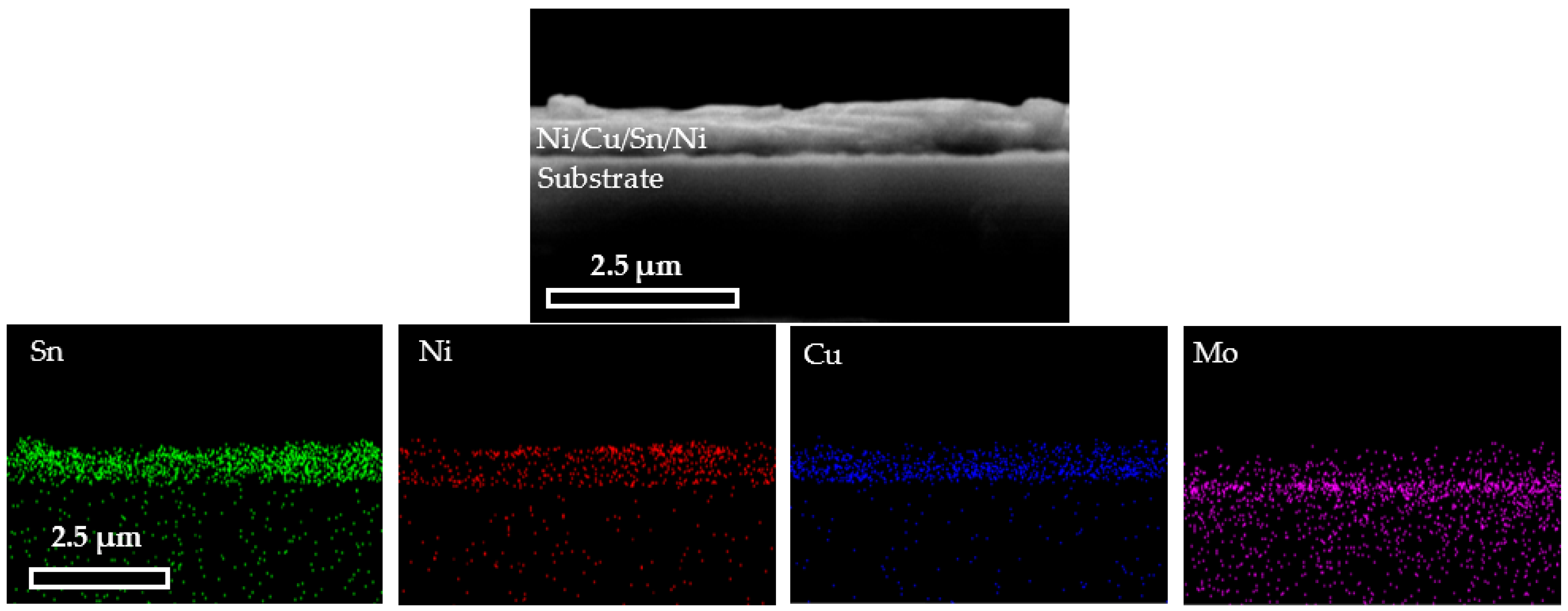
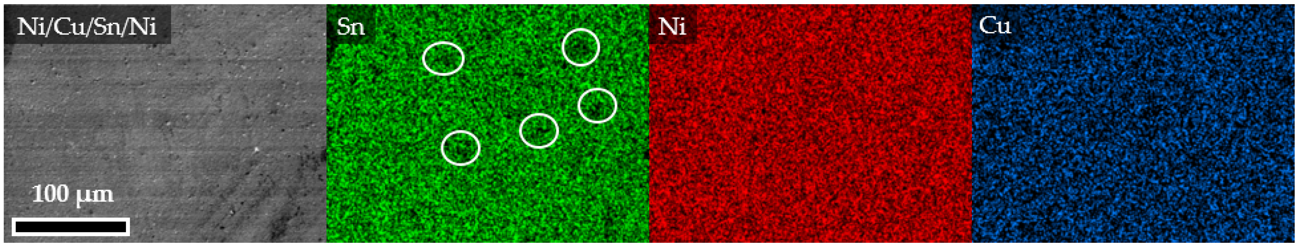
The Ni/Cu/Sn/Ni precursors had a uniform distribution of the deposited metal layers. The EDX mapping images showed a mutual diffusion of sequentially applied elements, which may indicate the formation of a binary or ternary intermetallic compound in the precursors.
(2)
It has been found that subsequent annealing in chalcogen vapor in air at 580 °C for 30 min makes it possible to obtain stable polycrystalline CNTSSe films.
(3)
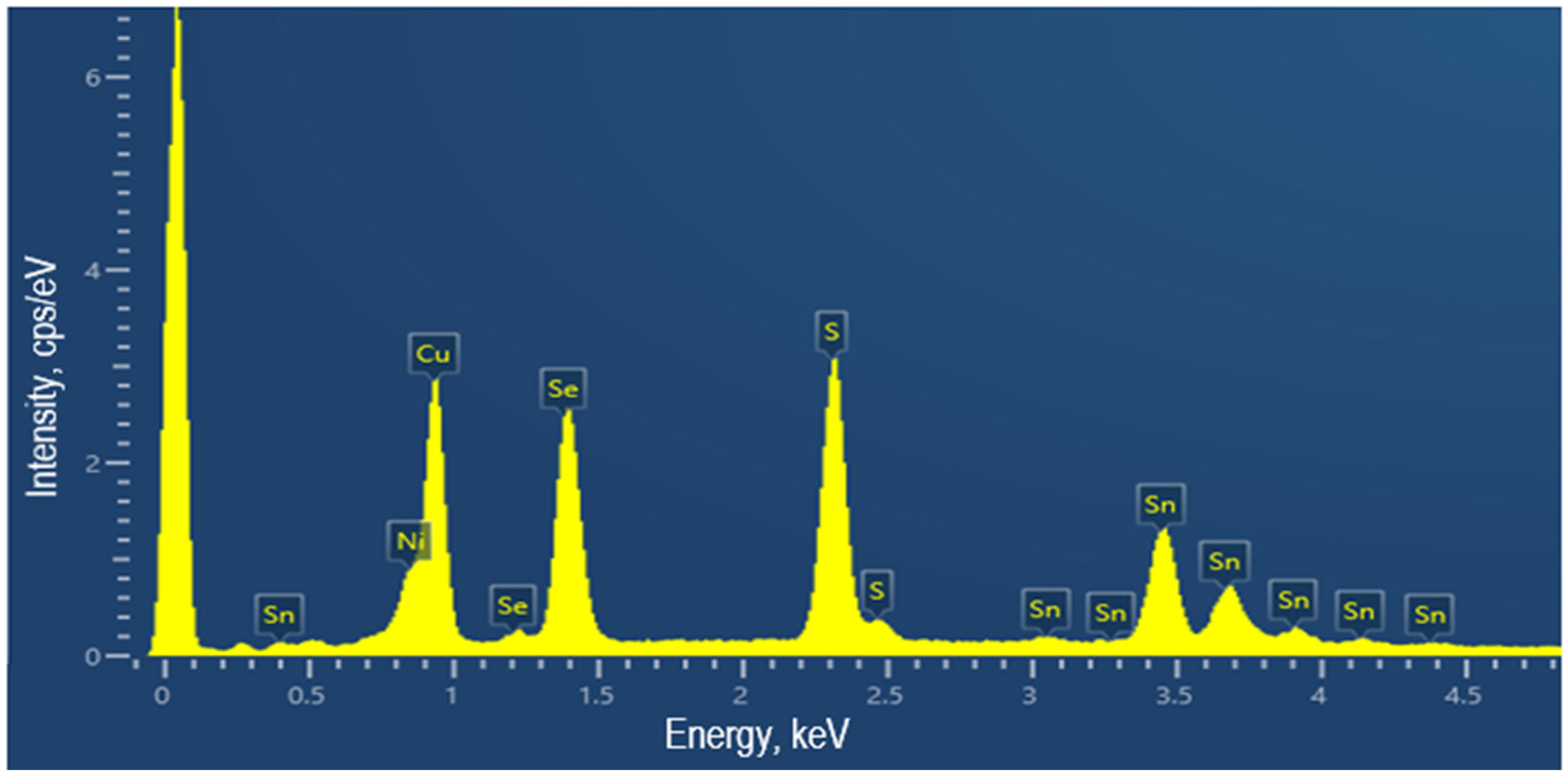
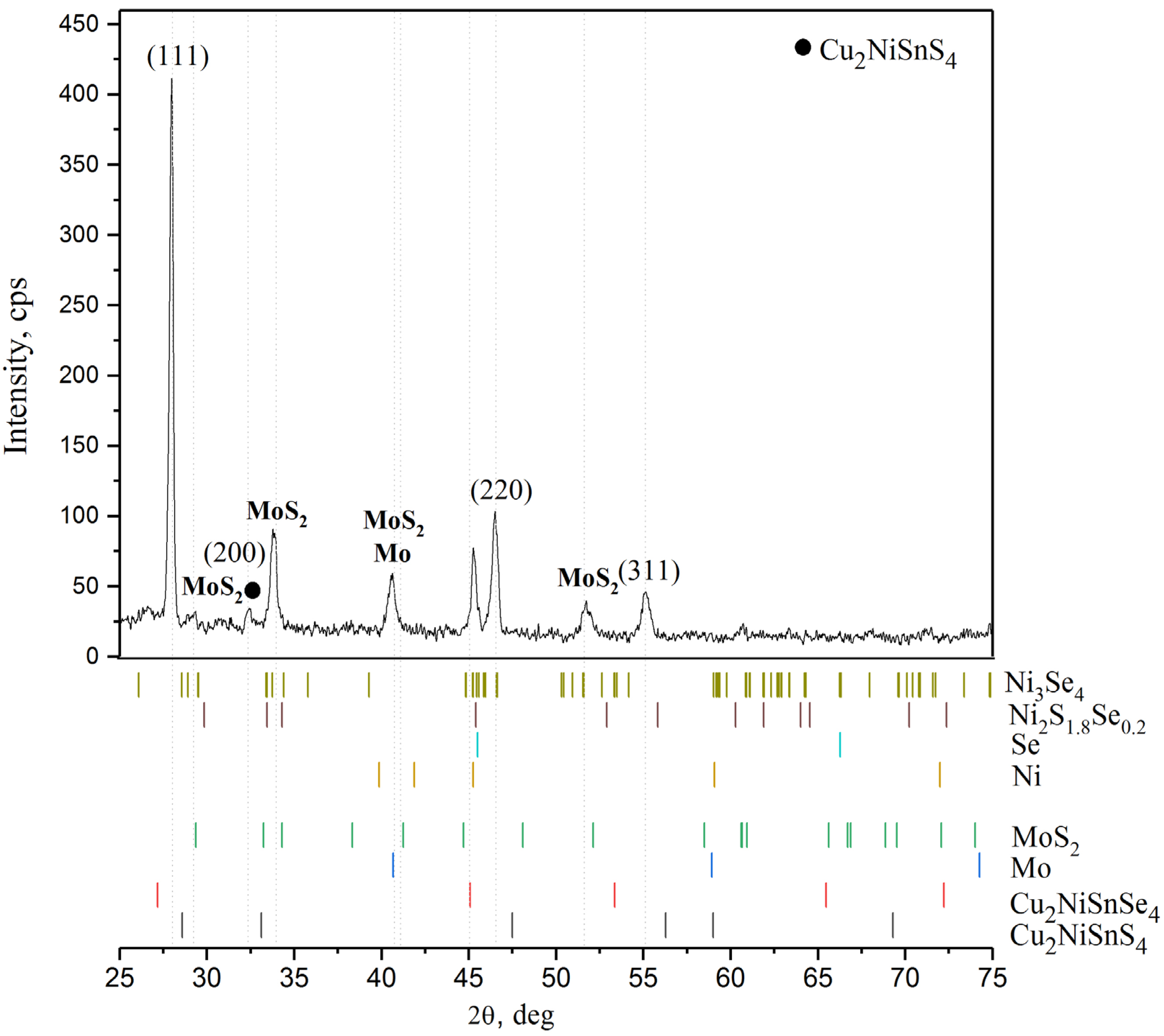
The CNTSSe films crystallized in a cubic structure. The films had small deviations from stoichiometry in the cation as well as an anion sub-lattice. The diffraction peaks from the CNTSSe on the X-ray patterns were between the positions of the peaks from CNTSe and CNTS. The calculated unit cell parameter for CNTSSe (a = 0.551(7) nm) was between the values for CNTSe and CNTS, and was closer to the values for CNTS. This was due to the higher content of sulfur in the films than that of selenium. Using X-ray diffraction, along with the CNTSSe main phase and CNTS phase, the presence of the Ni2S1.8Se0.2 or Ni3Se4 phase was detected. No characteristic peaks corresponding to other impurities such as Cu(S,Se), Sn(S,Se) or Cu2Sn(S,Se)3 were observed at the detection limit of the XRD apparatus. This shows the phase purity and good quality of the films.
(4)
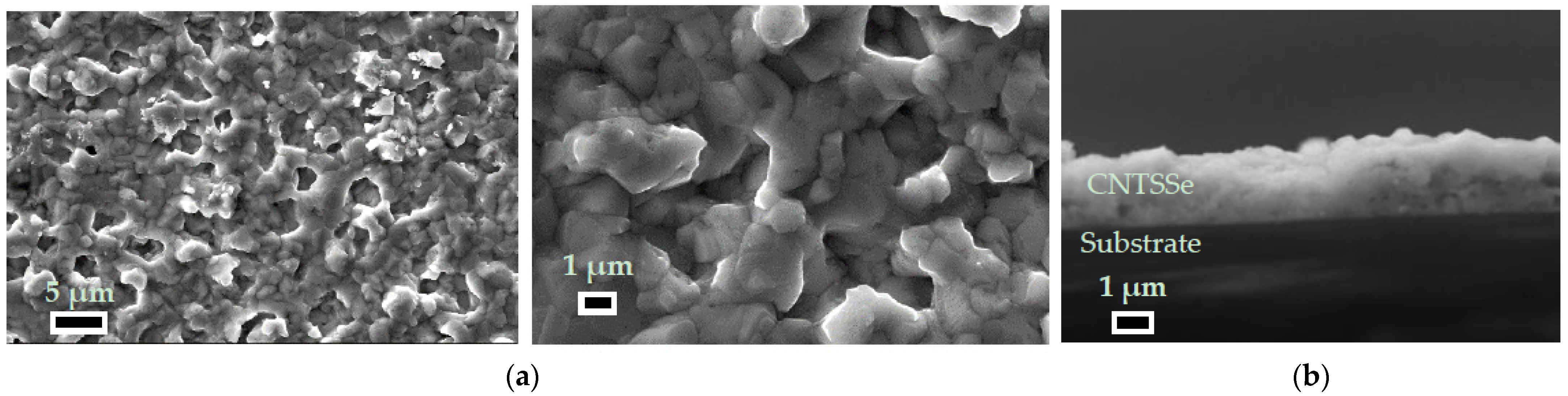
Annealing of the precursors led to an increase in their thickness from 700 to 900 nm to ~2.4 μm due to the insertion of sulfur and selenium atoms in the crystal lattice. It was found that the surface of the CNTSSe films is a homogeneous structure with densely packed large crystals and single pores.
Thus, the obtained results demonstrate the production of the CNTSSe thin films using the proposed method, which can be improved by more precise control of the composition of the initial precursors and heat-treatment conditions.

Author Contributions

Conceptualization, A.V.S., V.V.R., V.F.G., and M.V.G.; Methodology, A.V.S. and T.N.A.; Software, A.V.S., T.N.A., and E.L.T.; Validation, A.V.S., V.V.R., and V.F.G.; Formal analysis, A.V.S., T.N.A., E.L.T., T.I.Z., A.V.T., and S.V.T.; Investigation, A.V.S., T.N.A., and V.V.R.; Resources, A.V.S., T.N.A., E.L.T., T.I.Z., A.V.T., and S.V.T.; Data curation, A.V.S.; Writing—original draft preparation, A.V.S. and T.N.A.; Writing—review and editing, A.V.S., V.V.R., V.F.G., M.V.G., and E.L.T.; Visualization, A.V.S.; Supervision, A.V.S.; Project administration, A.V.S., T.N.A., V.V.R., T.I.Z., A.V.T., and S.V.T.; Funding acquisition, A.V.S., T.N.A., V.V.R., E.L.T., and S.V.T. All authors have read and agreed to the published version of the manuscript.

Funding

This research was financed by the Belarusian Republican Foundation for Basic Research (grant number T21PM-033) and the Russian Foundation for Basic Research (grant number 20-58-04005).

Institutional Review Board Statement

Not applicable.

Informed Consent Statement

Informed consent was obtained from all subjects involved in the study.

Data Availability Statement

Not applicable.

Conflicts of Interest

The authors declare no conflict of interest.

References

  1. Green, M.A.; Dunlop, E.D.; Hohl-Ebinger, J.; Yoshita, M.; Kopidakis, N.; Hao, X. Solar cell efficiency tables (version 59). Prog. Photovolt. 2022, 30, 3–12. [Google Scholar] [CrossRef]
  2. Alzahrani, G.S.; Alzahrani, F.S.; Ahmed, M. Nahhas Study of the Specific Factors Effecting the PV Solar Cell’s Efficiency in Saudi Arabia. Sustain. Energy 2022, 8, 6–11. [Google Scholar] [CrossRef]
  3. Moskowitz, P.D.; Fthenakis, V.M. Toxic Materials Released from Photovoltaic Modules During Fires. Health Risks. Sol. Cells 1990, 29, 63–71. [Google Scholar] [CrossRef]
  4. Green, M.A. Estimates of Te and In prices from direct mining of known ores. Prog. Photovolt. Res. Appl. 2009, 17, 347–359. [Google Scholar] [CrossRef]
  5. Stanchik, A.V.; Gremenok, V.F.; Juskenas, R.; Tyukhov, I.I.; Tivanov, M.S.; Fettkenhauer, C.; Shvartsman, V.V.; Giraitis, R.; Hagemann, U.; Lupascu, D.C. Effects of selenization time and temperature on the growth of Cu2ZnSnSe4 thin films on a metal substrate for flexible solar cells. Sol. Energy 2019, 178, 142–149. [Google Scholar] [CrossRef]
  6. Stanchik, A.V.; Tivanov, M.S.; Tyukhov, I.I.; Juskenas, R.; Korolik, O.V.; Gremenok, V.F.; Saad, A.M.; Naujokaitis, A. Temperature dependence of Raman scattering in the Cu2ZnSnSe4 thin films on a Ta foil substrate. Sol. Energy 2020, 201, 480–488. [Google Scholar] [CrossRef]
  7. Li, X.; Zhuang, D.; Zhang, N.; Zhao, M.; Yu, X.; Liu, P.; Weiab, Y.; Renab, G. Achieving 11.95% efficient Cu2ZnSnSe4 solar cells fabricated by sputtering a Cu–Zn–Sn–Se quaternary compound target with a selenization process. J. Mater. Chem. 2019, 7, 9948–9957. [Google Scholar] [CrossRef]
  8. Shockley, W.; Queisser, H.J. Detailed balance limit of efficiency of p-n junction solar cells. J. Appl. Phys. 1961, 32, 510–519. [Google Scholar] [CrossRef]
  9. Tampo, H.; Kim, S.; Nagai, T.; Shibata, H.; Niki, S. Improving the open circuit voltage through surface oxygen plasma treatment and 11.7% efficient Cu2ZnSnSe4 solar cel. ACS Appl. Mater. Interfaces 2019, 11, 13319–13325. [Google Scholar] [CrossRef]
  10. Taskesen, T.; Neerken, J.; Schoneberg, J.; Pareek, D.; Steininger, V.; Parisi, J.; Gütay, L. Device Characteristics of an 11.4% CZTSe Solar Cell Fabricated from Sputtered Precursors. Adv. Energy Mater. 2018, 8, 1703295. [Google Scholar] [CrossRef]
  11. Ghosh, A.; Thangavel, R.; Rajagopalan, M. First-Principles Study of Structural Stability and Optical Properties of Cu2XSnY4 (X = Fe, Co, Ni; Y = S, Se) for Photovoltaic Applications. Energy Environ. Focus 2014, 3, 142–151. [Google Scholar] [CrossRef]
  12. Ozel, F.; Sarılmaz, A.; Istanbullu, B.; Aljabour, A.; Kus, M.; Sonmezoglu, S. Penternary chalcogenides Cu2MSn(SeS)4 (M= Zn+2 and Co+2) nanocrystals as catalytic materials for efficient counter electrodes in dye-synthesized solar cells. Sci. Rep. 2016, 6, 29207. [Google Scholar] [CrossRef] [PubMed]
  13. Yüksel, O.F.; Ozel, F.; Akın, Ü.; Tugluoglu, N. Structural, optical and dispersion studies on Cu2NiSn(SSe)4 nanocrystals thin films. Phys. B Condens. Matter 2022, 625, 413530. [Google Scholar] [CrossRef]
  14. Rondiya, S.; Wadnerkar, N.; Jadhav, Y.; Jadkar†, S.; Haram, S.; Kabir, M. Structural, Electronic, and Optical Properties of Cu2NiSnS4: A Combined Experimental and Theoretical Study toward Photovoltaic Applications. Chem. Mater. 2017, 29, 3133–3142. [Google Scholar] [CrossRef]
  15. Ghosh, A.; Chaudhary, D.K.; Biswas, A.; Thangavel, R.; Udayabhanuc, G. Solution-processed Cu2XSnS4 (X = Fe, Co, Ni) photo-electrochemical and thin film solar cells on vertically grown ZnO nanorod arrays. RSC Adv. 2016, 6, 115204–115212. [Google Scholar] [CrossRef]
  16. Khattak, Y.H.; Baig, F.; Soucase, B.M.; Beg, S.; Gillani, S.R.; Ahmed, S. Efficiency enhancement of novel CNTS/ZnS/Zn(O,S) thin film solar cell. Optik 2018, 171, 453–462. [Google Scholar] [CrossRef]
  17. Hameed, T.A.; Cao, W.; Abdelrazek, E.M.; El Zawawi, I.K.; Mansour, B.A.; Elsayed-Ali, H.E. Effect of substrate temperature on properties of Cu(In,Ga,Al)Se2 films grown by magnetron sputtering. J. Mater. Sci. Mater. Electron. 2015, 27, 3209–3216. [Google Scholar] [CrossRef]
  18. Hameed, T.A.; Cao, W.; Mansour, B.A.; Elzawaway, I.K.; Abdelrazek, E.-M.M.; Elsayed-Ali, H.E. Properties of Cu(In,Ga,Al)Se2 thin films fabricated by magnetron sputtering. J. Vac. Sci. Technol. A Vac. Surf. Film. 2015, 33, 031201. [Google Scholar] [CrossRef]
  19. Volobujeva, O.; Bereznev, S.; Raudoja, J.; Otto, K.; Pilvet, M.; Mellikov, E. Synthesis and characterization of Cu2ZnSnSe4 thin films prepared via a vacuum evaporation-based route. Thin Solid Films 2013, 535, 48–51. [Google Scholar] [CrossRef]
  20. Broussillou, C.; Viscogliosi, C.; Rogee, A.; Angle, S.; Grand, P.P.; Bodnar, S.; Debauche, C.; Allary, J.L.; Bertrand, B.; Guillou, C.; et al. Statistical Process Control for Cu(In,Ga)(S,Se)2 electrodeposition-based manufacturing process of 60 × 120 cm2 modules up to 14.0% efficiency. In Proceedings of the 42nd Photovoltaic Specialists Conference (PVSC), New Orleans, LV, USA, 14–19 June 2015. [Google Scholar] [CrossRef]
  21. Rosoiu, S.P.; Costovici, S.; Moise, C.; Petica, A.; Anicai, L. Electrodeposition of ternary Sn-Cu-Ni alloys as lead-free solders using deep eutectic solvents. Electrochim. Acta 2021, 398, 139339. [Google Scholar] [CrossRef]
  22. Kondrotas, R. Electrochemical Deposition of Cu-Zn-Sn Precursor and Formation of Cu2ZnSnSe4 Solar Cell. Ph.D. Disserster, Vilniaus Universitetas, Vilnius, Lithuania, 2015; 153p. [Google Scholar]
  23. Hansen, R.M. Adherent Electroplating on Molybdenum. Ph.D. Thesis, Newark College of Engineering, Newark, NJ, USA, 1952; 41p. [Google Scholar]
  24. Miettinen, J. Thermodynamic description of the Cu–Ni–Sn system at the Cu–Ni side. Calphad 2003, 27, 309–318. [Google Scholar] [CrossRef]
  25. Juškėnas, R.; Niaura, G.; Mockus, Z.; Kanapeckaitė, S.; Giraitis, R.; Kondrotas, R.; Naujokaitis, A.; Stalnionis, G.; Pakštas, V.; Karpavičienė, V. XRD studies of an electrochemically co-deposited Cu-Zn-Sn precursor and formation of a Cu2ZnSnSe4 absorber for thin-film solar cells. J. Alloy. Compd. 2016, 655, 281–289. [Google Scholar] [CrossRef]
  26. Copper-Nickel Alloys: Properties, Processing, Applications. Available online: https://www.copper.org/applications/marine/cuni/properties/DKI_booklet.html (accessed on 18 July 2022).
  27. Isacfranklin, M.; Yuvakkumar, R.; Ravi, G.; Hong, S.I.; Shini, F.; Thambidurai, M.; Dang, C.; Velauthapillai, D. Marigold flower like structured Cu2NiSnS4 electrode for high energy asymmetric solid state supercapacitors. Natureresearch 2020, 10, 19198. [Google Scholar] [CrossRef] [PubMed]
  28. Dridi, S.; Bitri, N.; Mahjoubi, S.; Chaabouni, F.; Ly, I. One-step spray of Cu2NiSnS4 thin films as absorber materials for photovoltaic applications. J. Mater. Sci. Mater. Electron. 2020, 31, 7193–7199. [Google Scholar] [CrossRef]
  29. Aitelhaj, D.; Elkissani, A.; Elyaagoubi, M.; Aitdads, H.; Welatta, F.; Nkhaili, L.; Chaib, H.; Outzourhit, A. Development of Cu2NiSnS4 based thin film solar cells without a sulfurization step. Mater. Sci. Semicond. Process. 2020, 107, 104811. [Google Scholar] [CrossRef]
  30. Dehghania, Z.; Shadrokh, Z. Structural and optical properties of Cu2M(M: Zn, Fe, Co, Ni)SnSe4 nanoparticles synthesized via heating up method. Int. J. Light Electron. Opt. 2018, 169, 242–248. [Google Scholar] [CrossRef]
  31. Cui, Y.; Deng, R.; Wang, G.; Pan, D. A general strategy for synthesis of quaternary semiconductor Cu2MSnS4 (M= Co2+, Fe2+, Ni2+, Mn2+) nanocrystals. J. Dyn. Artic. 2012, 22, 23136. [Google Scholar] [CrossRef]
  32. Yang, C.L.; Chen, Y.H.; Lin, M.; Wu, S.L.; Li, L.; Liu, W.C.; Wu, X.S.; Zhang, F.M. Structural, optical and magnetic properties of Cu2NiSnS4 thin films deposited by facile one-step electrodeposition. Mater. Lett. 2016, 166, 101–104. [Google Scholar] [CrossRef]
  33. Beraich, M.; Taibi, M.; Guenbour, A.; Zarrouk, A.; Bellaouchou, A.; Fahoume, M. Synthesis of Tetragonal Cu2NiSnS4 Thin Film via Low-Cost Electrodeposition Method: Effect of Ni2+ Molarity. J. Electron. Mater. 2020, 49, 728–735. [Google Scholar] [CrossRef]
  34. Stanchik, A.V.; Baraishuk, S.M.; Zhygulin, D.V.; Pyatlitski, A.N.; Trukhanava, E.L.; Chumak, V.A. Phase composition and microstructure of Cu2ZnSn(S,Se)4 thin films. Proc. Fr. Skorina Gomel State Univ. 2021, 3, 143–149. [Google Scholar]
  35. Stanchik, A.; Chumak, V.; Trukhanava, E.; Baraishuk, S. Crystal structure and optical properties of Cu2ZnSn(S,Se)4 thin films. BSPU Bulletin. Ser. 2021, 2, 13–19. [Google Scholar]
  36. Liu, T.; Diao, P.; Lin, Z.; Wang, H. Sulfur and selenium doped nickel chalcogenides as efficient and stable electrocatalysts for hydrogen evolution reaction: The importance of the dopant atoms in and beneath the surface. Nano Energy 2020, 74, 104787. [Google Scholar] [CrossRef]
  37. Awodugba, A.O.; Ibiyemi, A.A.; Ajayi, J.O. Effect of grain size on the electrical transport mechanism for zinc doped CdS thin films. Int. J. Sci. Res. Manag. Stud. 2014, 1, 234–241. [Google Scholar] [CrossRef]
  38. Daniela, T.O.; Unob, U.E.; Isahc, K.U.; Ahmadud, U. Optimization of electrical conductivity of SnS thin film of 0.2 <t ≤0.4 µm thickness for field effect transistor application. Rev. Mexic. Física 2021, 67, 263–268. [Google Scholar] [CrossRef]
Figure 1. The SEM and EDX mapping images of the cross-section of the Ni/Cu/Sn/Ni precursors on a glass/Mo substrate.
Coatings 12 01198 g001
Figure 2. The top view of the SEM and EDX mapping images of the Ni/Cu/Sn/Ni precursors.
Coatings 12 01198 g002
Figure 3. A typical EDX spectrum CNTSSe thin films on a glass/Mo substrate.
Coatings 12 01198 g003
Figure 4. The top view (a) and cross-section (b) SEM mapping images of the CNTSSe thin films on a glass/Mo substrate.
Coatings 12 01198 g004
Figure 5. The top view SEM and EDX mapping images of the CNTSSe thin films.
Coatings 12 01198 g005
Figure 6. A typical X-ray pattern of the CNTSSe thin films on a glass/Mo substrate. Reference patterns from COD: Ni3Se4 (no. 96-900-9245), Ni2S1.8Se0.2 (no. 96-153-8792), Se (no. 96-901-3135), Ni (no. 96-901-3008), MoS2 (no. 96-153-5541), Mo (no. 96-901-1607), Cu2NiSnSe4 (no. 00-026-0551), Cu2NiSnS4 (no. 00-026-0552).
Coatings 12 01198 g006
Table 1. The elemental composition and atomic ratio of the CNTSSe thin films.
Elemental Composition, at.%Ratio
CuNiSnSeSCu/(Ni + Sn)Ni/SnS/(S + Se)
20.2011.6012.4722.7233.000.840.930.59
Publisher’s Note: MDPI stays neutral with regard to jurisdictional claims in published maps and institutional affiliations.

