Article

Step-By-Step Development of Vertically Aligned Carbon Nanotubes by Plasma-Enhanced Chemical Vapor Deposition

by
Octavian-Gabriel Simionescu
1,2,*,
Oana Brîncoveanu
1,
Cosmin Romaniţan
1,
Silviu Vulpe
1 and
Andrei Avram
1
1
National Institute for Research and Development in Microtechnologies, 126A Erou Iancu Nicolae Street, 077190 Voluntari, Ilfov, Romania
2
Doctoral School of Physics, University of Bucharest, 077125 Măgurele, Ilfov, Romania
*
Author to whom correspondence should be addressed.
Coatings 2022, 12(7), 943; https://doi.org/10.3390/coatings12070943
Submission received: 17 June 2022 / Revised: 28 June 2022 / Accepted: 1 July 2022 / Published: 3 July 2022
(This article belongs to the Section Laser Coatings)

Abstract

:
In this work, the growth process of self-sustained vertically aligned carbon nanotubes (VA-CNTs) is investigated in full: from bare Si wafers to fully grown VA-CNTs on 4″ wafers. Each developmental step, from supporting and catalyst layers’ depositions to CNT growth, is analyzed through X-ray diffraction, X-ray reflectivity, and scanning electron microscopy, respectively. The crystalline structure of the titanium nitride supporting layer is investigated through grazing incidence X-ray diffraction, while X-ray reflectivity provides information regarding the density, thickness, and roughness of the titanium nitride layer via extended Fourier analysis. Further, the nickel layers’ and CNTs’ morphologies are investigated by scanning electron microscopy.

1. Introduction

Carbon nanotubes (CNTs) were formally discovered by S. Iijima in 1991 [1] when he reported the growth of “microtubules of graphitic carbon” on the cathode of a DC arc–discharge reactor. They may have been obtained as early as 1976 when Oberlin et al. [2] reported similar structures, although their paper did not attract as much interest at the time [3] as these types of structures drew more fascination only after the empirical discovery of the C 60 Buckminsterfullerene in 1985 by H. W. Kroto, J. R. Heath, S. C. O’Brien, R. F. Curl, and R. E. Smalley [4]. CNTs can be found in the scientific literature either as tangled or vertically aligned (VA); single-walled or multiwalled when discussing the number of coaxial cylinders; or, more importantly, as metallic or semiconductors when viewed with respect to their chirality (i.e., armchair, zig-zag or helical) [3].
They possess a range of very attractive physicochemical properties [5], such as excellent mechanical strength [6,7,8], very good thermal conductivity and stability [9,10,11,12], and high electrical conductivity [13,14]. Due to their unique variety of properties, they have been studied in several fields of applications, ranging from battery and supercapacitor electrodes [15,16] to MW absorption [17], flexible electronics [18,19,20], heat dissipation [21,22], and various structures in nano-/micro-electromechanical systems (NEMS/MEMS) [23].
Three main techniques have been utilized over the years for CNT growth, namely, arc discharge [24], laser ablation [25], and chemical vapor deposition (CVD) [26,27]. In-depth reviews of the three methods are readily available [5,27,28] and they show that while the former two produce more qualitative nanotubes, the latter allows CNT growth at much lower temperatures (<1000 °C vs. >3000 °C). This makes CVD a much more suitable technique for large-scale growth and device integration. Therefore, the CVD method, along with its alternatives (e.g., thermal CVD (TCVD), plasma-enhanced CVD (PECVD), photothermal CVD, aerogel-supported CVD, aerosol-assisted CVD, laser-assisted CVD, alcohol catalytic CVD, and remote PECVD), have seen increased use lately, with TCVD and PECVD being the most studied two [29]. With the inclusion of plasma in the growth step, PECVD offers the advantage of relatively lower substrate temperatures due to the additional plasma energy source contributing to precursor dissociation [29], the ability to adjust the orientation with respect to the substrate as was demonstrated by Merkulov et al. with carbon nanofibers [30], as well as providing improved control over properties such as chirality, length, and diameter [31]. Based on the growth parameters and the nature of the catalyst and supporting layer/substrate, VA-CNTs can grow via one of two mechanisms: tip growth or base/root growth [5,28,29,32].
We report here the full intricate process of self-sustained VA-CNT growth via radio frequency (RF) PECVD on a TiN supporting layer with a Ni catalyst, while detailing the importance and influence of each step. This work describes CNT PECVD growth from bare Si or thermally oxidized Si (SiO 2 /Si) wafers to fully grown VA-CNTs via the tip growth mechanism.

2. Materials and Methods

For the present work, both bare Si wafers and thermally oxidized (300 nm-layer) Si wafers were used. Initial tests were performed on diced Si samples ( 2 × 2 cm 2 ) and later, the process was scaled up to full 4″ Si and SiO 2 /Si wafers. All samples were chemically cleaned in a Piranha solution, neutralized in deionized water, and N 2 dried prior to the depositions.

2.1. RF Magnetron Sputtering of TiN and Ni Layers

The TiN and Ni layers were deposited directly onto the substrate by RF magnetron sputtering (MS) with the PlasmaLab System 400 from Oxford Instruments, Abingdon, UK. The TiN layer deposition was carried out reactively, from a 154 mm-diameter Ti target (Testbourne Ltd., Basingstoke, UK), by introducing both Ar (99.999% purity) and N 2 (99.9999% purity) in the reaction chamber and igniting a RF (13.56 MHz) plasma. Ar plays the role of the main sputtering/dissociative gas, while N 2 is introduced with the purpose of bonding with the sputtered Ti particles and, consequently, forming TiN molecules. A base pressure of 10 7 Torr is reached prior to the deposition, after which Ar and N 2 are introduced into the chamber and the plasma is ignited at 30 mTorr. After ignition, the pressure is lowered to the desired value. The N 2 percentage in the Ar:N 2 gas mixture was varied from ∼28 to 14 and finally to 9%, while the pressure and RF power were kept constant during the deposition at ∼2 mTorr and 350 W, respectively. The Ni layer was deposited through a nonreactive sputtering process, using only Ar plasma, directly from a high-purity target (154 mm-diameter) at 500 W RF power and 30 mTorr pressure. Both the TiN and Ni depositions were carried out at a substrate temperature of 50 °C.

2.2. PECVD Growth of VA-CNTs

CNT growth is achieved with the PECVD technique, using the Nanofab 1000 system from Oxford Instruments, Abingdon, UK. The samples are introduced in the preheated (650 °C) reactor, set to a base pressure of 10 3 Torr, through a load-lock chamber (10 2 Torr). The temperature is raised at the desired value by 15 °C min 1 in an Ar:NH 3 atmosphere, after which an annealing step in NH 3 is performed. Alternatively, the samples are heated in a H 2 atmosphere followed by a H 2 plasma step. The CNT growth is accomplished in a CH 4 :NH 3 atmosphere, in a parallel plate reactor, by employing a RF plasma. The process parameters are presented in-depth, alongside the whole steps, in Table 1.

2.3. Characterization

The morphology and growth evolution of the supporting TiN layer, the Ni catalyst layer, and of the CNTs were systematically investigated through scanning electron microscopy (SEM) with the Nova NanoSEM 630 microscope from FEI Company, Hillsboro, OR, USA. Both top-view and cross-section micrographs were acquired in order to determine their thickness, as well as their evolution with respect to the different treatments and growth parameters. The acquired SEM cross-section micrographs were also used to compare the diameters and heights of the developed CNTs. X-ray diffraction (XRD) investigations of the TiN layers were made using a 9-kW SmartLab diffractometer (Rigaku Corporation, Tokyo, Japan) with a rotating anode. The system is equipped with an X-ray source that provides a monochromatic beam with a wavelength of 0.154 nm. First, grazing incidence X-ray diffraction (GIXRD) patterns were recorded by keeping the X-ray source at 0.5 , while the detector scanned from 25 to 90 . Second, X-ray reflectivity (XRR) data were obtained in the θ / 2 θ scan mode at low angles.

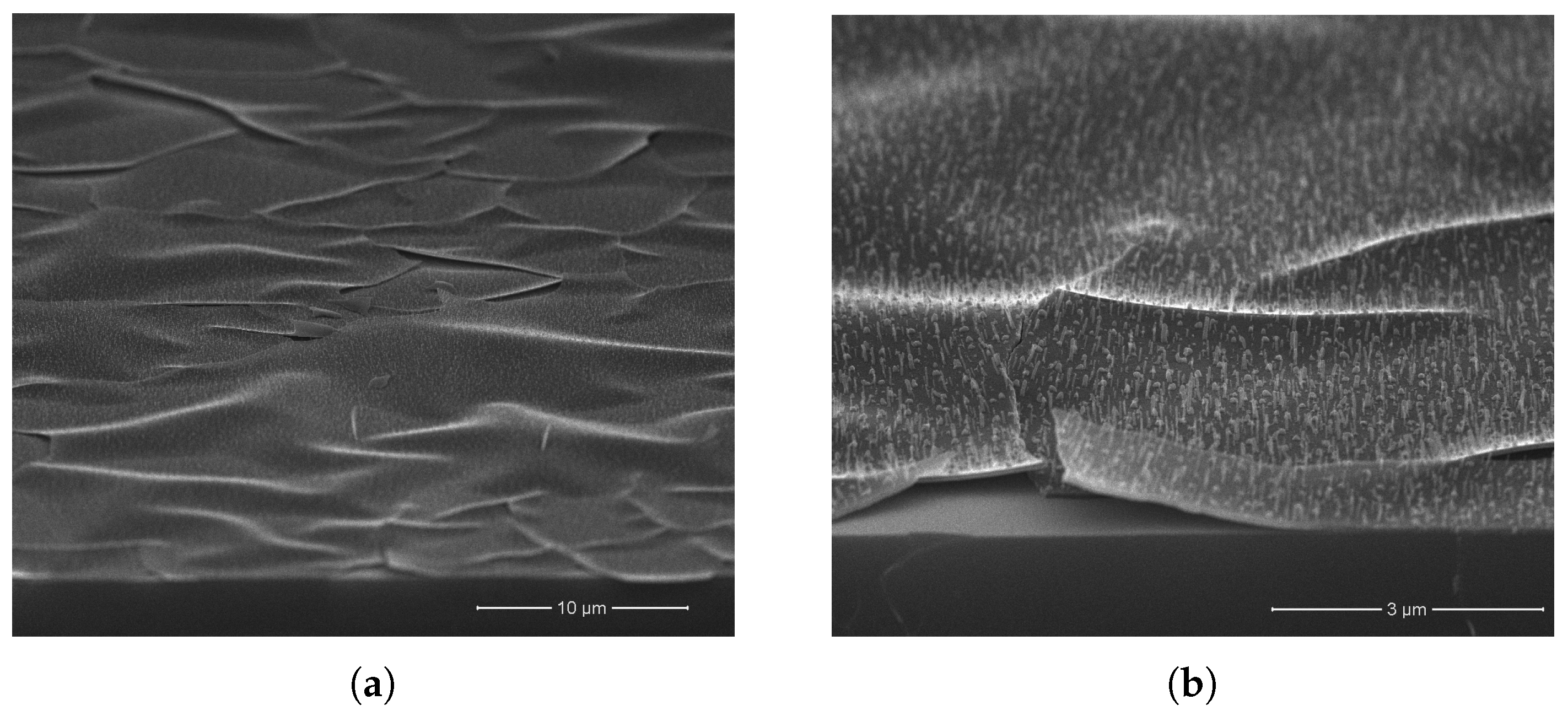
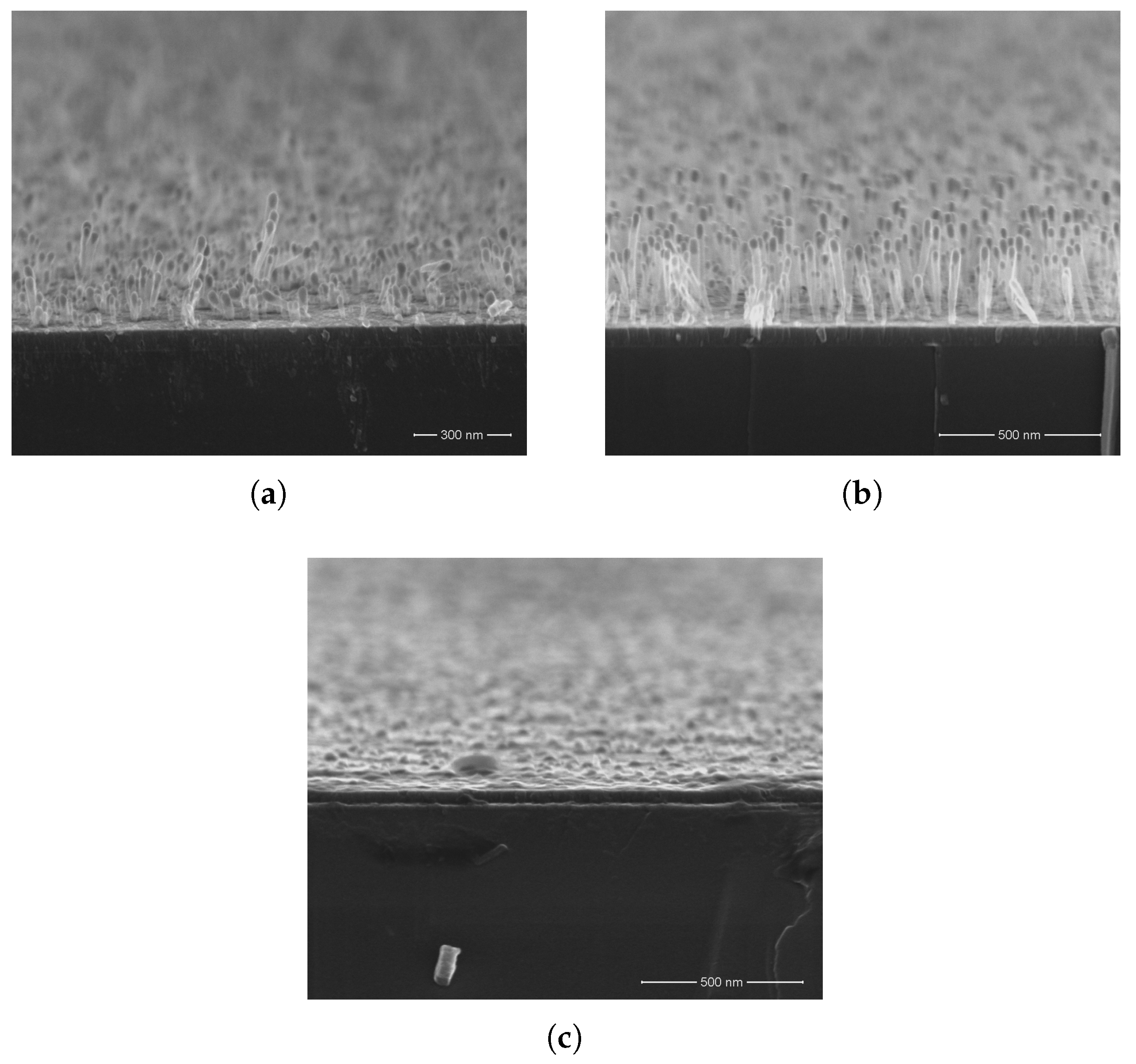
3. Results and Discussion

The TiN thin film plays the role of an antidiffusion barrier for the catalyst, preventing the Ni layer from diffusing into the SiO 2 /Si at high temperatures. Initial tests were performed on a TiN supporting layer deposited on Si substrates with an already developed process of 28% N 2 during the plasma step. Later on, it was discovered that the aforementioned TiN layer, while forming a continuous thin film on Si substrates, has poor adhesion to SiO 2 . Even in the case of the bare Si substrates, the supporting layer cracks when exposed to atmospheric pressure after thermal annealing and processing at 750–900 °C (Figure 1) when using 4″ wafers. This is most probably due to induced mechanical stress during the RF MS deposition caused, in turn, by the high nitrogen content [33]. Hence, further investigations were performed and the TiN deposition was optimized by reducing the N 2 flow rate [34].
The X-ray diffraction patterns of the as-deposited supporting layer (Figure 2) indicate multiple diffraction peaks located at 36.2 , 42.51 , 61.3 , and 73.5 that can be assigned unambiguously to the (111), (200), (220), and (311) reflections of the TiN phase, respectively, with lattice constants a = b = c = 0.42 nm and belonging to the Fm-3m(225) space group. The sharp peak seen at ≈51 corresponds to the Si wafer.
The mean crystallite size of the TiN layers was evaluated with the Scherrer equation, which relates the peak broadening, β , to the size of the crystalline domains, τ , as follows [35]:
β τ = k λ τ cos θ ,
where k is the shape factor of the crystalline domains, taken as 0.93 in our case, and λ represents the X-ray wavelength, which is 0.154 nm. Using Equation (1), the following values for crystallite size were obtained when bare Si substrates were used: 3.9 nm (Ar:N 2 = 25:10 sccm), 7.9 nm (Ar:N 2 = 30:5 sccm), and 8.4 nm (Ar:N 2 = 30:3 sccm). For the SiO 2 /Si substrates, the obtained values were 2.8 nm (Ar:N 2 = 25:10 sccm), 10.9 nm (Ar:N 2 = 30:5 sccm), and 9.8 nm (Ar:N 2 = 30:3 sccm).
Further, in order to determine the TiN density and its thickness, X-ray reflectivity was employed, varying the incidence angle from 0 to 5 (Figure 3a,b). As can be observed, each XRR profile presents a critical angle, where the X-ray scattering suffers a strong intensity fall-off. The position of the critical angle, θ c , is 0.261 (Ar:N 2 = 25:10 sccm), 0.312 (Ar:N 2 = 30:5 sccm), and 0.289 (Ar:N 2 = 30:3 sccm) for the samples on Si substrates, while for the samples on SiO 2 /Si substrates, θ c = 0 . 279 (Ar:N 2 = 25:10 sccm), 0.295 (Ar:N 2 = 30:5 sccm), and 0.279 (Ar:N 2 = 30:3 sccm). As is well-known, the value of the critical angle is related to the sample density [36,37]. Accordingly, the following values for TiN density were computed: 3.4 g cm 3 (Ar:N 2 = 25:10 sccm), 4.9 g cm 3 (Ar:N 2 =30:5 sccm), and 4.3 g cm 3 (Ar:N 2 = 30:3 sccm) when using Si substrates, and 3.9 g cm 3 (Ar:N 2 = 25:10 sccm), 4.4 g cm 3 (Ar:N 2 = 30:5 sccm), and 3.9 g cm 3 (Ar:N 2 = 30:3 sccm) when using SiO 2 /Si substrates. The process with 14% N 2 in the plasma step yielded the density value closest to the theoretical density of 5.24 g cm 3 .
To gain additional information regarding the thickness and roughness of the TiN layer, extended Fourier analysis was used on the X-ray reflectograms (Figure 3c,d). The thickness was calculated based on the period of periodic fringes, called Kiessig fringes [38]. According to the original paper of H. Kiessig [39,40], the appearance of intensity oscillations is understood from the same formalism developed for thin-film optics, i.e., maximum intensities are observed whenever the phase difference, Δ, between the reflected and the refracted beam is a multiple of the wavelength, λ . Furthermore, the roughness is determined by the variation of the scattered intensity with respect to the incidence angle, I ( θ ) . For instance, the intensity of the specular scattering for an ideal surface, without roughness, obeys the θ 4 dependence, whereas, for a rough surface, the dependence becomes steeper [37]. The as-deposited TiN layers present themselves with excellent surface roughness, with sub-nanometer values. The results given by the extended Fourier analysis are listed in Figure 3c,d.
The XRD investigations (Figure 2) of the samples developed with the new 9 and 14% N 2 processes show a much better defined TiN crystalline structure both on the Si and on the SiO 2 /Si substrates. A higher growth rate (≈2 times higher) is also observed compared with the initial recipe. Moving forward, a 64 ± 4 nm-thick TiN film, developed with the 14% N 2 process, was used as supporting layer. Ni acts as a catalyst for the CNT growth and is initially deposited as a continuous layer that later diffuses on the substrate and forms small catalytic centers (CCs), either by thermal annealing in a reducing atmosphere (i.e., NH 3 ), or by H 2 plasma treatment. The treatment of the catalyst layer is an important step in CNT growth, as the CCs’ diameters and areal density directly influence the growth of nanotubes. Here, the combination of parameters (i.e., temperature, time, gas partial pressure, and others), as well as the nature of the supporting layer [41], influence not only the areal density and morphology of the CNT growth but also the growth mechanism itself (i.e., tip/base growth) through surface diffusion energy, free surface energy, and/or binding energy. Another factor that can influence the CCs’ diameter is the thickness of the as-synthesized thin film. Small-diameter CNTs require a very small catalyst thickness and so, the SEM investigations of such layers can prove quite difficult due to approaching the apparatus’ detection limit. Hence, a series of tests were conducted to establish the Ni layer’s deposition rate. As the substrate oscillates 90 left-to-right ( 45 + 45 ) in a parallel plane to the target for better uniformity, the deposition rate was determined with respect to one oscillation/sweep. Deposition tests of 5, 10, and 15 sweeps were accomplished, resulting in Ni thicknesses of ≊14 ± 2, 32 ± 3 , and 52 ± 3 nm, respectively. This concludes in a deposition rate r ( o ) 3.15 ± 0.3 nm osc 1 or r ( t ) 0.4 nm s 1 , when considering the sweep period of approximately eight seconds. With this in mind, the NH 3 annealing step was tested on a ≈6–7 nm-thick Ni layer that was deposited with a plasma strike step at 30 mTorr and a single additional sweep at 2 mTorr. The film was treated at various temperatures in NH 3 atmosphere to produce the desired CCs. As can be seen in Figure 4a,b, the resulting CCs have incompatible dimensions with small-scale CNT growth, with diameters of ≈100–200 nm and heights of ≈15–70 nm. The Ni growth was further reduced to only the plasma strike step to produce an ≈2–3 nm-thick layer, which results in CCs with much more favorable dimensions for CNT growth, with diameters of ≈10–35 nm and heights of ≈20–30 nm (Figure 4c,d).
The CNT growth was performed with CH 4 as the carbon source and NH 3 acting as a reducing agent for the Ni catalyst as well as an etchant for the amorphous carbon. The 200 W RF plasma is used both to dissociate the gas molecules and to infer a vertical preferential growth to the nanotubes due to the electric field’s orientation. The NH 3 gas flow rate was varied from 25 to 50 and ultimately to 100 sccm, while the CH 4 gas flow rate was kept constant at 70 sccm for a one hour growth time, to determine an optimal gas ratio for CNT growth (Figure 5). In the case of 25 sccm NH 3 flow rate, the CNTs appear to grow in a bundlelike pattern due to insufficient etchant for the adsorbed amorphous carbon. Furthermore, the individual bundles have a low height uniformity and poor structure as the etching particles are quickly depleted by a percentage of CNTs, and the growth of the remainder of nanotubes is stopped/altered by amorphous carbon capping. At the other extreme, at 100 sccm NH 3 flow rate, a few forming structures are observed at the surface but the process is clearly etch-dominant and few to no fully grown CNTs are observed. Finally, the optimal gas ratio proved to be around 70:50 sccm (CH 4 :NH 3 ), where an equilibrium between etching and growth is achieved.
Growth steps were performed at various substrate temperatures, ranging from 750 to 900 °C with a 50 °C increment. The best results were observed at 750 and 800 °C, where the resulted CNTs have an ≈20–30 nm-diameter and heights of ≈230–260 nm and ≈440–500 nm, respectively (Figure 6a,b). Above that temperature, the CNTs’ areal density suffers a severe drop, with few to no CNTs observed on the surface at 850 and 900 °C, respectively (Figure 6c,d). This is due to an exceedingly high surface diffusion energy, caused in turn by the high substrate temperature that prompts the hydrocarbon radicals to be reabsorbed into the plasma faster than they can dissociate and diffuse through the CCs [42].
Further on, tests concerning the localized growth of the established VA-CNTs processes were performed. This was accomplished by applying a mechanical mask with square holes (0.1 × 0.1, 0.15 × 0.15, 0.3 × 0.3, 0.5 × 0.5, 1 × 1, 2 × 2, and 3 × 3 mm) on the substrate before the Ni deposition. After the catalyst layer deposition, the mask is removed and the sample is introduced in the PECVD reactor for the CNT growth, in the same manner as before. A darker color gradient, due to CNT growth, can be observed in the desired areas even with the naked eye (Figure 7a). SEM investigations reveal VA-CNTs in the exposed areas during Ni deposition, while the rest of the surface presents no growth whatsoever. The preferentially grown nanotubes are uniform and relatively spaced from each other (Figure 7b–d) compared with other VA-CNTs in the scientific literature, which are usually densely packed in order to sustain themselves vertically.
For the scaled-up version of CNTs, the growth was accomplished on 4″ SiO 2 /Si wafers and, to allow for a lower growth temperature, the catalyst treatment step was changed from a five-minute NH 3 thermal annealing to a 2–2.5-min H 2 plasma step. The plasma allows a lower substrate temperature to be used as it provides additional energy for molecule dissociation in the plasma phase and additional energy to the substrate through ion bombardment, for the Ni particles’ diffusion. Hence, successful self-sustained VA-CNT growth was accomplished at 700 °C by employing a two-minute H 2 plasma treatment step. After several tests at a fixed 80 sccm CH 4 gas flow rate and a varied NH 3 gas flow rate (from 30 to 60 sccm, with an increment of 10 sccm), the gas flow ratio was further tuned for growth on 4″ substrates. For a 30-min growth time, a gas flow ratio of CH 4 :NH 3 = 80:40 sccm proved to be optimal (Figure 8a), yielding VA-CNTs of ≈120 nm height and diameters ranging from ≈15 to 30 nm. However, when increasing the growth time up to two hours, only a few nanotubes appear to have heights of over 180–200 nm, while the majority appear to have stopped their development in the early stages (Figure 8b). This indicates a direct correlation between the growth time and the precursor–etchant balance [43]. To further investigate this phenomenon, the test presented in Figure 6b was repeated with an increased five-hour growth step. The newly developed CNTs reach heights of up to ≈1.3 μm but are highly irregular and have a much poorer areal surface density (Figure 8c). The growth rate also appears to have approximately halved (≈8.3 nm min−1 vs. ≈4.3 nm min−1), when considering the tallest CNTs from both samples (Figure 6b vs. Figure 8c). This confirms our initial suspicion that with an increased growth time, a higher influx of etching agent may be required to prevent the amorphous carbon capping.

4. Conclusions

The intricacies of VA-CNT growth by RF-PECVD are presented in this work, with insights into each developmental step. The deposition of the TiN supporting layer by RF MS and its crystalline structure is investigated, together with the influence of the Ni layer thickness on the CNTs’ diameters. Gas flow ratios and substrate temperatures during PECVD growth were also investigated and their impact on nanotube capping is discussed. It is also noted that the choice of supporting layer(s) can influence the catalyst’s diffusion rate on the surface due to the free surface energy, while the combination of supporting layer–catalyst has an impact not only on the diffusion rate but also on the growth mechanism. The substrate temperature is another key variable in surface diffusion rate as well as in the CNT growth, as was evidenced here. A correlation between gas ratios, growth time, and CNT capping shows that at shorter growth times, a smaller quantity of etching agent may be used.
Through a better understanding of CNT’s growth mechanism, one can achieve better control of their areal density directly in the growth phase, without the additional need of a previous catalyst patterning step. This can simplify the production of VA-CNT based devices and greatly improve their tunability.

Author Contributions

Conceptualization, O.-G.S. and A.A.; methodology, A.A.; validation, O.-G.S. and A.A.; formal analysis, O.-G.S. and C.R.; investigation, O.-G.S., O.B., C.R., S.V. and A.A.; resources, A.A.; data curation, O.-G.S.; writing—original draft preparation, O.-G.S. and C.R.; writing—review and editing, O.-G.S., O.B., C.R., S.V. and A.A.; visualization, O.-G.S.; supervision, A.A.; project administration, A.A.; funding acquisition, A.A. All authors have read and agreed to the published version of the manuscript.

Funding

This research was funded from contract no. 77/08.09.2016 under the structural funds project Partnership in Exploitation of Key Essential Technologies, using an interactive platform with competitive companies—SMIS 2014+ code 105623.

Data Availability Statement

The data presented in this study are available upon reasonable request request from the corresponding author.

Acknowledgments

The authors would like to extend their gratitude to Gabriel Crăciun for his help in acquiring a portion of the SEM micrographs.

Conflicts of Interest

The authors declare no conflict of interest.

Abbreviations

The following abbreviations are used in this manuscript:
VA-CNTsVertically aligned carbon nanotubes
DCDirect current
MWMicrowave
NEMSNano-electromechanical systems
MEMSMicro-electromechanical systems
CVDChemical vapor deposition
TCVDThermal chemical vapor deposition
PECVDPlasma-enhanced chemical vapor deposition
RFRadio frequency
MSMagnetron sputtering
SEMScanning electron microscopy
XRDX-ray diffraction
GIXRDGrazing incidence X-ray diffraction
XRRX-ray reflectivity
FFTFast Fourier transform
CCsCatalytic centers

References

  1. Iijima, S. Helical microtubules of graphitic carbon. Nature 1991, 354, 56–58. [Google Scholar] [CrossRef]
  2. Oberlin, A.; Endo, M.; Koyama, T. Filamentous growth of carbon through benzene decomposition. J. Cryst. Growth 1976, 32, 335–349. [Google Scholar] [CrossRef]
  3. Terrones, M. Science and Technology of the Twenty-First Century: Synthesis, Properties, and Applications of Carbon Nanotubes. Ann. Rev. Mater. Res. 2003, 33, 419–501. [Google Scholar] [CrossRef]
  4. Kroto, H.W.; Heath, J.R.; O’Brien, S.C.; Curl, R.F.; Smalley, R.E. C60: Buckminsterfullerene. Nature 1985, 318, 162–163. [Google Scholar] [CrossRef]
  5. Yan, Y.; Miao, J.; Yang, Z.; Xiao, F.X.; Yang, H.B.; Liu, B.; Yang, Y. Carbon nanotube catalysts: Recent advances in synthesis, characterization and applications. Chem. Soc. Rev. 2015, 44, 3295–3346. [Google Scholar] [CrossRef] [PubMed]
  6. Treacy, M.M.J.; Ebbesen, T.W.; Gibson, J.M. Exceptionally high Young’s modulus observed for individual carbon nanotubes. Nature 1996, 381, 678–680. [Google Scholar] [CrossRef]
  7. Salvetat, J.P.; Bonard, J.M.; Thomson, N.H.; Kulik, A.J.; Forró, L.; Benoit, W.; Zuppiroli, L. Mechanical properties of carbon nanotubes. Appl. Phys. A-Mater. Sci. Process. 1999, 69, 255–260. [Google Scholar] [CrossRef]
  8. Yu, M.F.; Lourie, O.; Dyer, M.J.; Moloni, K.; Kelly, T.F.; Ruoff, R.S. Strength and Breaking Mechanism of Multiwalled Carbon Nanotubes Under Tensile Load. Science 2000, 287, 637–640. [Google Scholar] [CrossRef] [PubMed] [Green Version]
  9. Che, J.; Çagin, T.; Goddard, W.A. Thermal conductivity of carbon nanotubes. Nanotechnology 2000, 11, 65–69. [Google Scholar] [CrossRef]
  10. Hone, J.; Llaguno, M.C.; Nemes, N.M.; Johnson, A.T.; Fischer, J.E.; Walters, D.A.; Casavant, M.J.; Schmidt, J.; Smalley, R.E. Electrical and thermal transport properties of magnetically aligned single wall carbon nanotube films. Appl. Phys. Lett. 2000, 77, 666–668. [Google Scholar] [CrossRef]
  11. Fujii, M.; Zhang, X.; Xie, H.; Ago, H.; Takahashi, K.; Ikuta, T.; Abe, H.; Shimizu, T. Measuring the Thermal Conductivity of a Single Carbon Nanotube. Phys. Rev. Lett. 2005, 95, 065502. [Google Scholar] [CrossRef]
  12. Li, Q.; Liu, C.; Wang, X.; Fan, S. Measuring the thermal conductivity of individual carbon nanotubes by the Raman shift method. Nanotechnology 2009, 20, 145702. [Google Scholar] [CrossRef]
  13. Fischer, J.E.; Johnson, A.T. Electronic properties of carbon nanotubes. Curr. Opin. Solid State Mater. Sci. 1999, 4, 28–33. [Google Scholar] [CrossRef]
  14. McEuen, P.; Fuhrer, M.; Park, H. Single-walled carbon nanotube electronics. IEEE Trans. Nanotechnol. 2002, 1, 78–85. [Google Scholar] [CrossRef] [Green Version]
  15. Schnorr, J.M.; Swager, T.M. Emerging Applications of Carbon Nanotubes. Chem. Mater. 2011, 23, 646–657. [Google Scholar] [CrossRef] [Green Version]
  16. De Volder, M.F.L.; Tawfick, S.H.; Baughman, R.H.; Hart, A.J. Carbon Nanotubes: Present and Future Commercial Applications. Science 2013, 339, 535–539. [Google Scholar] [CrossRef] [PubMed] [Green Version]
  17. Liu, Y.; Zhang, Y.; Zhang, C.; Huang, B.; Li, Y.; Lai, W.; Wang, X.; Liu, X. Low temperature preparation of highly fluorinated multiwalled carbon nanotubes activated by Fe3O4 to enhance microwave absorbing property. Nanotechnology 2018, 29, 365703. [Google Scholar] [CrossRef]
  18. Yamada, T.; Hayamizu, Y.; Yamamoto, Y.; Yomogida, Y.; Izadi-Najafabadi, A.; Futaba, D.N.; Hata, K. A stretchable carbon nanotube strain sensor for human-motion detection. Nat. Nanotechnol. 2011, 6, 296–301. [Google Scholar] [CrossRef]
  19. Park, S.; Vosguerichian, M.; Bao, Z. A review of fabrication and applications of carbon nanotube film-based flexible electronics. Nanoscale 2013, 5, 1727–1752. [Google Scholar] [CrossRef]
  20. Sun, X.; Sun, J.; Li, T.; Zheng, S.; Wang, C.; Tan, W.; Zhang, J.; Liu, C.; Ma, T.; Qi, Z.; et al. Flexible Tactile Electronic Skin Sensor with 3D Force Detection Based on Porous CNTs/PDMS Nanocomposites. Nano-Micro Lett. 2019, 11, 57. [Google Scholar] [CrossRef] [Green Version]
  21. Kordás, K.; Tóth, G.; Moilanen, P.; Kumpumäki, M.; Vähäkangas, J.; Uusimäki, A.; Vajtai, R.; Ajayan, P.M. Chip cooling with integrated carbon nanotube microfin architectures. Appl. Phys. Lett. 2007, 90, 123105. [Google Scholar] [CrossRef] [Green Version]
  22. Fu, Y.; Nabiollahi, N.; Wang, T.; Wang, S.; Hu, Z.; Carlberg, B.; Zhang, Y.; Wang, X.; Liu, J. A complete carbon-nanotube-based on-chip cooling solution with very high heat dissipation capacity. Nanotechnology 2012, 23, 045304. [Google Scholar] [CrossRef]
  23. Dahmardeh, M.; Vahdani Moghaddam, M.; Hian Tee, M.; Nojeh, A.; Takahata, K. The effects of three-dimensional shaping of vertically aligned carbon-nanotube contacts for micro-electro-mechanical switches. Appl. Phys. Lett. 2013, 103, 231606. [Google Scholar] [CrossRef]
  24. Keidar, M.; Levchenko, I.; Arbel, T.; Alexander, M.; Waas, A.M.; Ostrikov, K.K. Increasing the length of single-wall carbon nanotubes in a magnetically enhanced arc discharge. Appl. Phys. Lett. 2008, 92, 043129. [Google Scholar] [CrossRef]
  25. Kingston, C.T.; Simard, B. Recent Advances in Laser Synthesis of Single-Walled Carbon Nanotubes. J. Nanosci. Nanotechnol. 2006, 6, 1225–1232. [Google Scholar] [CrossRef]
  26. Endo, M.; Takeuchi, K.; Igarashi, S.; Kobori, K.; Shiraishi, M.; Kroto, H.W. The production and structure of pyrolytic carbon nanotubes (PCNTs). J. Phys. Chem. Solids 1993, 54, 1841–1848. [Google Scholar] [CrossRef]
  27. Kumar, M.; Ando, Y. Chemical Vapor Deposition of Carbon Nanotubes: A Review on Growth Mechanism and Mass Production. J. Nanosci. Nanotechnol. 2010, 10, 3739–3758. [Google Scholar] [CrossRef] [Green Version]
  28. See, C.H.; Harris, A.T. A Review of Carbon Nanotube Synthesis via Fluidized-Bed Chemical Vapor Deposition. Ind. Eng. Chem. Res. 2007, 46, 997–1012. [Google Scholar] [CrossRef]
  29. Ahmad, M.; Silva, S.R.P. Low temperature growth of carbon nanotubes—A review. Carbon 2020, 158, 24–44. [Google Scholar] [CrossRef]
  30. Merkulov, V.I.; Melechko, A.V.; Guillorn, M.A.; Simpson, M.L.; Lowndes, D.H.; Whealton, J.H.; Raridon, R.J. Controlled alignment of carbon nanofibers in a large-scale synthesis process. Appl. Phys. Lett. 2002, 80, 4816–4818. [Google Scholar] [CrossRef] [Green Version]
  31. Kato, T.; Hatakeyama, R. Growth of Single-Walled Carbon Nanotubes by Plasma CVD. J. Nanotechnol. 2010, 2010, 256906. [Google Scholar] [CrossRef] [Green Version]
  32. Meyyappan, M.; Delzeit, L.; Cassell, A.; Hash, D. Carbon nanotube growth by PECVD: A review. Plasma Sources Sci. Technol. 2003, 12, 205–216. [Google Scholar] [CrossRef]
  33. Carbonari, M.; Martinelli, J. Effects of hot isostatic pressure on titanium nitride films deposited by physical vapor deposition. Mater. Res. 2001, 4, 163–168. [Google Scholar] [CrossRef] [Green Version]
  34. Chang, C.C.; Nogan, J.; Yang, Z.P.; Kort-Kamp, W.J.M.; Ross, W.; Luk, T.S.; Dalvit, D.A.R.; Azad, A.K.; Chen, H.T. Highly Plasmonic Titanium Nitride by Room-Temperature Sputtering. Sci. Rep. 2019, 9, 15287. [Google Scholar] [CrossRef] [Green Version]
  35. Patterson, A.L. The Diffraction of X-Rays by Small Crystalline Particles. Phys. Rev. 1939, 56, 972–977. [Google Scholar] [CrossRef]
  36. Bowen, D.; Tanner, B. High Resolution X-ray Diffractometry And Topography; CRC Press, Taylor and Francis Group: Boca Raton, FL, USA, 1998; p. 252. [Google Scholar] [CrossRef]
  37. Als-Nielsen, J.; McMorrow, D. Elements of Modern X-ray Physics; John Wiley & Sons: Hoboken, NJ, USA, 2011; p. 434. [Google Scholar]
  38. Birkholz, M. Thin Film Analysis by X-ray Scattering; Wiley-VCH: Hoboken, NJ, USA, 2005; p. 378. [Google Scholar]
  39. Kiessig, H. Untersuchungen zur Totalreflexion von Röntgenstrahlen. Ann. Phys. 1931, 402, 715–768. [Google Scholar] [CrossRef]
  40. Kiessig, H. Interferenz von Röntgenstrahlen an dünnen Schichten. Ann. Phys. 1931, 402, 769–788. [Google Scholar] [CrossRef]
  41. Xiao, Y.; Ahmed, Z.; Ma, Z.; Zhou, C.; Zhang, L.; Chan, M. Low Temperature Synthesis of High-Density Carbon Nanotubes on Insulating Substrate. Nanomaterials 2019, 9, 473. [Google Scholar] [CrossRef] [Green Version]
  42. Il’in, O.I.; Il’ina, M.V.; Rudyk, N.N.; Fedotov, A.A.; Ageev, O.A. Vertically Aligned Carbon Nanotubes Production by PECVD. In Perspective of Carbon Nanotubes; Saleh, H.E.D., El-Sheikh, S.M.M., Eds.; IntechOpen: Rijeka, Croatia, 2019; Chapter 5. [Google Scholar] [CrossRef] [Green Version]
  43. Na, N.; Kim, D.Y.; So, Y.G.; Ikuhara, Y.; Noda, S. Simple and engineered process yielding carbon nanotube arrays with 1.2 × 1013 cm−2 wall density on conductive underlayer at 400 °C. Carbon 2015, 81, 773–781. [Google Scholar] [CrossRef]
Figure 1. Cross-section micrographs at (a) 7000× and (b) 30,000× magnification of a cracked/wrinkled TiN supporting layer after being subjected to CNT growth at 700 °C.
Coatings 12 00943 g001
Figure 2. Grazing incidence X-ray diffraction (GIXRD) spectra of as-deposited TiN thin films processed under different Ar:N 2 gas flow rates on (a) Si and (b) SiO 2 /Si substrates.
Coatings 12 00943 g002
Figure 3. X-ray reflectivity (XRR) spectra for as-deposited TiN films processed under different Ar:N 2 flow rates on (a) Si and (b) SiO 2 substrates; the density, ρ , is calculated from the critical angle. Fast Fourier transform (FFT) spectra of (c) the films on Si substrates and (d) the films on SiO 2 substrates; h represents the film thickness and R is the surface roughness.
Coatings 12 00943 g003
Figure 4. Scanning electron microscopy (SEM) micrographs at (a,c) 120,000× and (b,d) 100,000× magnification of the Ni catalyst layer after thermal annealing at 800 °C in NH 3 atmosphere: (a) cross-section and (b) top-view of the ∼6–7 nm-thick annealed Ni layer; (c) cross-section and (d) top-view of the ∼2–3 nm-thick annealed Ni layer.
Coatings 12 00943 g004
Figure 5. Cross-section SEM micrographs at 150,000× magnification of CNT samples grown at 750 °C and a fixed 70 sccm CH 4 gas flow rate while the NH 3 gas flow rate was varied as follows: (a) 25 sccm, (b) 50 sccm, and (c) 100 sccm.
Coatings 12 00943 g005
Figure 6. Cross-section SEM micrographs at (ac) 100,000× and (d) 200,000× magnification of CNT samples grown with a fixed CH 4 :NH 3 = 70:50 sccm gas flow ratio at (a) 750 °C, (b) 800 °C, (c) 850 °C, and (d) 900 °C for 1 h.
Coatings 12 00943 g006
Figure 7. (a) Photograph of a sample where a color gradient is observable (evidenced by the red arrows) due to the localized growth of VA-CNTs. SEM micrographs at a 60 tilt angle and (b) 25,000×, (c) 50,000×, and (d) 100,000× magnification of the zones evidenced by red arrows in (a).
Coatings 12 00943 g007
Figure 8. Cross-section micrographs of VA-CNTs grown at (a) 700 °C with a two-minute H 2 plasma treatment step and a 30-min CH 4 :NH 3 (80:40) plasma step; (b) 700 °C with a two-min H 2 plasma treatment step and a 120-min CH 4 :NH 3 (80:40) plasma step; (c) 800 °C with a five-minute NH 3 thermal annealing step and a 300-min CH 4 :NH 3 (70:50) plasma step.
Coatings 12 00943 g008
Table 1. Plasma-enhanced chemical vapor deposition (PECVD) process parameters of vertically-aligned carbon nanotubes (VA-CNTs) with detailed steps.
Catalyst TreatmentStepHeating RateTemperatureTimePressureRF PowerGas Flow Rate [sccm]
(°C min−1)(°C)(min)(mTorr)(W)ArH2NH3CH4
NH3Heat-up15 650 100020050
Treatment700–9002–51000100
H2Heat-up15 650 1000200
Treatment700–9002–51000200200
Growth700–90030–300100020030–6070 & 80
Cool-down9 650 200
Publisher’s Note: MDPI stays neutral with regard to jurisdictional claims in published maps and institutional affiliations.

