Article

Dual-Band Terahertz Perfect Absorber Based on Metal Micro-Nano Structure

1
School of Physics, Changchun University of Science and Technology, Changchun 130022, China
2
Joint Laboratory for Extreme Conditions Matter Properties, Southwest University of Science and Technology, Mianyang 621010, China
*
Authors to whom correspondence should be addressed.
Coatings 2022, 12(5), 687; https://doi.org/10.3390/coatings12050687
Submission received: 20 April 2022 / Revised: 8 May 2022 / Accepted: 11 May 2022 / Published: 16 May 2022

Abstract

:
We propose a sub-wavelength range-based dual-band tunable ideal terahertz metamaterial perfect absorber. The absorber structure consists of three main layers, with the absorber layer consisting of a metal I-shaped structure. By simulating the incident wave absorbance of the structure, we found that the structure has more than 99% absorption peaks in both bands. In addition, we have investigated the relationship between structural absorbance and the structural geometrical parameters. We have studied the relationship between the thickness of the metal absorber layer h b and the absorbance of the metamaterial structure in the 4–14 THz band. Secondly, we have studied the relationship between the thickness of the SiO2 dielectric layer and structural absorbance. Afterwards, we have studied the relationship between the incident angle of the incident electromagnetic wave and structural absorbance. Finally, we have studied the relationship between the length of the metal structure and structural absorbance. The structure can be effectively used for detectors, thermal emitters, terahertz imaging and detection.

1. Introduction

The metamaterial absorber is a device that effectively absorbs incident radiation at operating wavelengths and converts it into other forms of energy, such as heat. Conventional absorbers are made of those whose absorptivity is innate, but metamaterial absorbers are mainly made of noble metals. With advances in metamaterial research, new opportunities for the development of absorption materials have opened up for wider applications in solar energy absorption [1,2], detectors [3,4], thermal emitters [5,6], terahertz imaging [7,8] and detection.
The first experimental realization of a metamaterial was made by Landy in 2008, in which they used a whole row of periodically arranged metallic structures as an absorber layer, with a metallic structure at the bottom and a dielectric layer in the middle [9]. They, experimentally, obtained an absorption rate of over 88% at 11.5 GHz and an operating frequency of 4% in the absorption band for this structure. Since then, researchers have researched metamaterials in various aspects, gradually extending the operating wavelengths of metamaterial-based absorbers to terahertz, visible, infrared and microwave [10,11,12,13,14,15,16], and gradually achieving multi-wavelength and broadband absorption. Wei et al. achieved perfect absorption through a grating structure covered by tungsten, which limits reflectivity through regional dipole resonance and surface plasma propagation patterns, creating two discrete absorption peaks at 670 nm and 957 nm, with absorption over 90% [17]. Perfect absorption was achieved by Wang, B.X. et al., using a three-layer base structure that allows two narrow-band absorption peaks at short discrete distances. The absorption peaks are, respectively, at 2.06 THz, 2.27 THz and 2.51 THz, with absorption about 100% [18]. Princy et al. used a double-concentric hexagonal split-ring structure, as a resonant cavity structure, to achieve five discrete narrow band absorption peaks in the terahertz band. The absorption peaks are, respectively, at 0.078 THz, 0.142 THz, 0.39 THz and 0.47 THz, with absorption about 100% [19]. Barzegar-Parizi proposed a dual-band absorber consisting of two types of single-unit periodic arrays. The absorption peaks are, respectively, at 1.2 THz and 2.7 THz, with absorption about 100% [20]. Huang, L. et al. designed a perfect absorber with a parallel I-shaped structure as its mental absorber layer, which is similar to the one we designed. Different from the structure in the paper, we used a thinner mental layer and a vertical arrangement. We can achieve more absorption in the direction of the magnetic field, to get multi-wavelength absorption. Besides what is mentioned above, there is some similar research presented in Table 1 [21,22,23,24,25]. In these studies, the structure of the absorber layer is relatively complex, such as a grating structure covered by tungsten, a double-concentric hexagonal split-ring structure, two types of single-unit periodic arrays, etc. Compared with these studies, the design of our structure is relatively simple for machining and production. In the meantime, this structure achieves dual-band absorption and a wider gap between absorption peaks.
As a branch of metamaterials, photonic crystals can also achieve perfect absorption. Wang, X. et al. proposed an effective method to achieve multi-channel perfect absorption in a visible light band, based on a 1D-topological-photonic-crystal heterostructure with graphene [26]. Kassa-Baghdouche, L. et al. present, in 2015, a novel design for a high quality (Q)-factor, nonlinear planar photonic crystal nanocavity, incorporating a silicon/polymer material that is well suited to ultrafast all-optical switching. In 2019, they proposed a liquid sensor based on the elliptical-hole planar photonic crystal nanocavities. Different from the metamaterial absorption structure introduced in this paper, the structure size of photonic crystals is, usually, approximate to their working wavelength [27,28]. The size of structure we designed in this paper is of a subwavelength scale.
However, more research is needed to achieve a perfect absorber with a multi-band absorption rate of 99% or more. In this paper, we have achieved a perfect absorber in the terahertz band, by using an absorber layer consisting of a reflective layer, a dielectric layer and a metallic I-shaped structure. By simulating the incident absorption of the structure, we find that the structure has more than 99% absorption peaks in both bands.

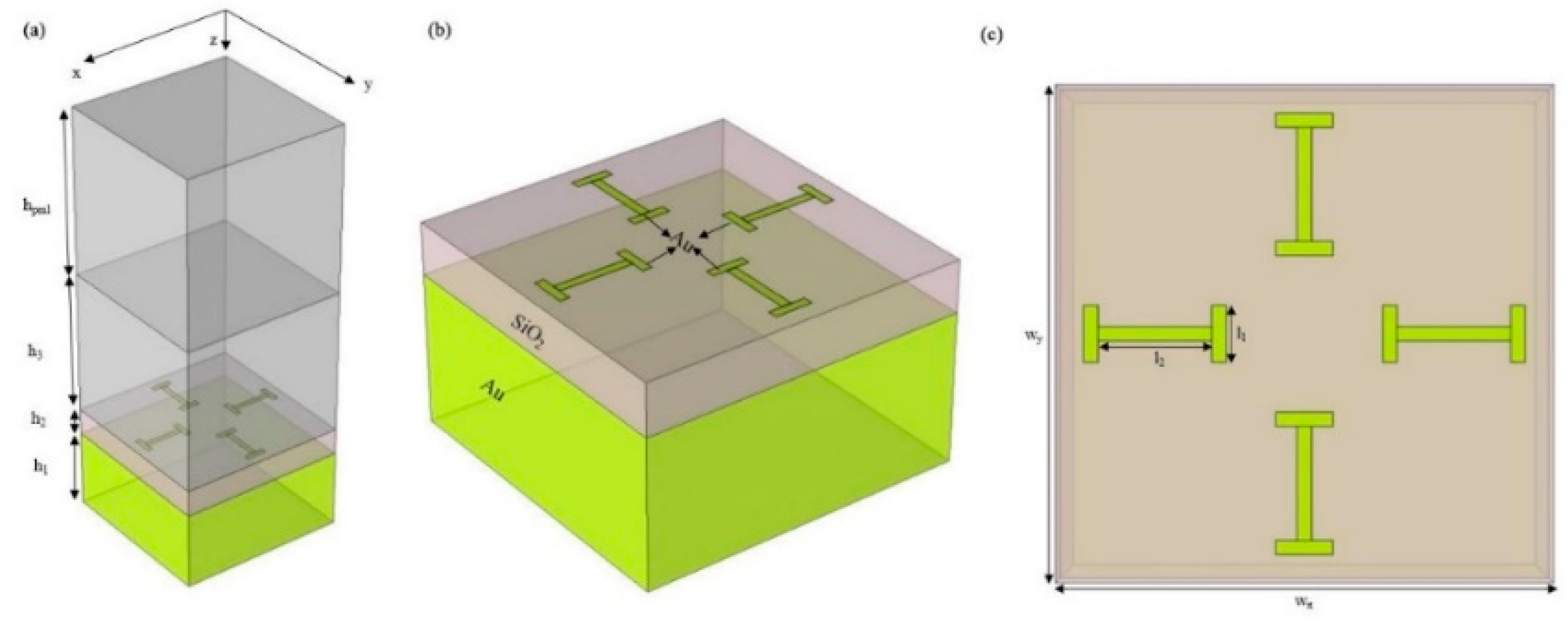
2. Unit Structure and Simulation Methods

In this work, we simulate the absorption characteristics of incident electromagnetic waves through the structure, by means of finite element analysis. The software we used to simulate the result is COMSOL. In the simulations, the absorption result of the absorber can be expressed by the equation A ( ω ) = 1 T ( ω ) R ( ω ) , where T ( ω ) is the transmittance and R ( ω ) is the reflectance. To achieve perfect absorption, both transmittance and reflectance need to be zero. To reduce the transmittance to zero, we placed a metal layer at the bottom. To eliminate transmitted light from the absorbing structures, we make the bottom layer of the absorbent structure thicker than the skin depth. The reflectivity can be expressed as:
S 11 = Z Z 0 Z + Z 0
Z = μ ε
Z 0 = μ 0 ε 0
where μ and ε denote the permittivity and permeability of the material, respectively, while μ 0 and ε 0 are the values in free space [29,30,31,32,33]. Impedance matching can be achieved, when the reflectivity of the structure reduces to zero.
In Equations (1)–(3), we know that when the surface impedance of the designed metamaterial structure matches the impedance of the air, the reflection of the metamaterial structure becomes 0. Therefore, when the impedance of the designed absorber structure meets Z = 1, we can obtain the reflection R = 0 and, finally, achieve the complete absorption of incident light by the designed metamaterial structure.
The coupling of the electric dipole to the magnetic resonance or the surface impedance of the metamaterial structure depends, mainly, on the thickness of the intermediate dielectric layer. Thus, by optimizing the thickness of the dielectric layer, we can achieve nearly 100% absorption of incident light. After calculation through COMSOL, we can, preliminarily, determine the geometric parameters of the result.
To achieve perfect absorption, the equivalent impedance of the structure needs to be equal to 1. Since the dielectric constant of the metal is negative at low frequencies, it is necessary to change the metal to control its dielectric constant. By changing the radius r of the metal wire and the distance between the metal wire, the degree of metal change will be affected, thus affecting the equivalent dielectric constant of the material. The metal absorbing layer acts as inductance. Due to the absorption spectrum obtained by the metal strip absorption layer being too narrow, in this paper we designed the metal absorption layer as I-shaped to achieve wider spectral absorption.
The structure of the metamaterial perfect absorber designed in this paper is shown in Figure 1a. It consists of five layers: the first is the Au, placed at the bottom. The thickness of this layer is h 1 = 16   μ m . The side length is w x = w y = 35   μ m ; the second layer is the SiO2 dielectric layer, with dielectric constant 2.13. The thickness of this layer is h 2 = 15.5   μ m ; the third layer is the Au absorber layer. The thickness of this layer is h b = 0.02   μ m . The geometrical parameters are l 1 = 18   μ m and l 2 = 2   μ m ; the fourth layer is the vacuum layer, with thickness h 3 = 30   μ m , the fifth layer is a perfectly matched layer, with a thickness of h p m l = 35   μ m .
In order to analyze and ensure the characteristics of the surface plasmons, there are four characteristic lengths: the propagation length of the surface plasmon polariton (SPP) δ S P P ; the wavelength of SPP λ S P P ; the depth of penetration of the electromagnetic field, related to the SPP mode, into the dielectric medium and metal δ d and δ m . Together, they describe the spatial scale range of surface plasmons, which we use as a basis for a series of studies. It can be derived directly from the dispersion equation.
At the metal–dielectric interface, the surface plasma dispersion relation can be written as follows:
k S P P ( ω ) = k 0 ε d ε m ( ω ) ε d + ε m ( ω )
λ S P P = 2 π k S P P = λ 0 ε d + ε m ε d ε m
where, k S P P and ε m represent the real parts of k S P P and ε m , respectively. It can be seen from the above equation that λ S P P is always less than the wavelength of light λ 0 , when in a vacuum. If a variety of periodic modulation structures are machined on a metal surface to control SPP, the period of the structure must be of the same order as λ S P P , and the transmission wavelength determines the size of the surface plasmon optical device.
The propagation length of SPP depends, mainly, on the imaginary part of the SPP wave vector, since the imaginary part of the dielectric constant corresponds to the loss of the metal (Equation (4)).
When the intensity of SPP along the transmission direction attenuates to 1/e, the transmission distance is (Equation (5)).
λ S P P determines the maximum-size upper limit of the SPP components and loops.
Metamaterials can be thought of as an infinite plane, formed by the metal/medium interface, and the depth of penetration through the medium can be calculated using the dispersion relationship. The depth of penetration of the electromagnetic field, related to the metamaterials mode into dielectric medium δ d , can be expressed as
δ d = 1 k 0 | ( ε m ) 2 ε d + ε m |
The depth of penetration of the electromagnetic field, related to the metamaterials mode into metal δ m , can be expressed as
δ m = 1 k 0 | ε d + ε m ( ε d ) 2 |
If the thickness of the metal film is less than δ m , the surface plasmon energy is not only confined to the metal surface, but also penetrates to the other side.
In the course of our study, we study the relationship between absorption performance and system structural parameters. In the course of our research, we make the structure extend wirelessly in the xy-plane, by setting periodic boundary conditions.

3. Results and Discussion

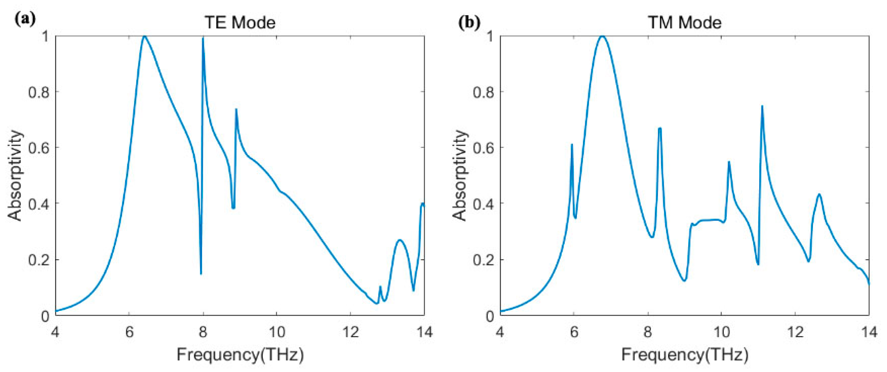
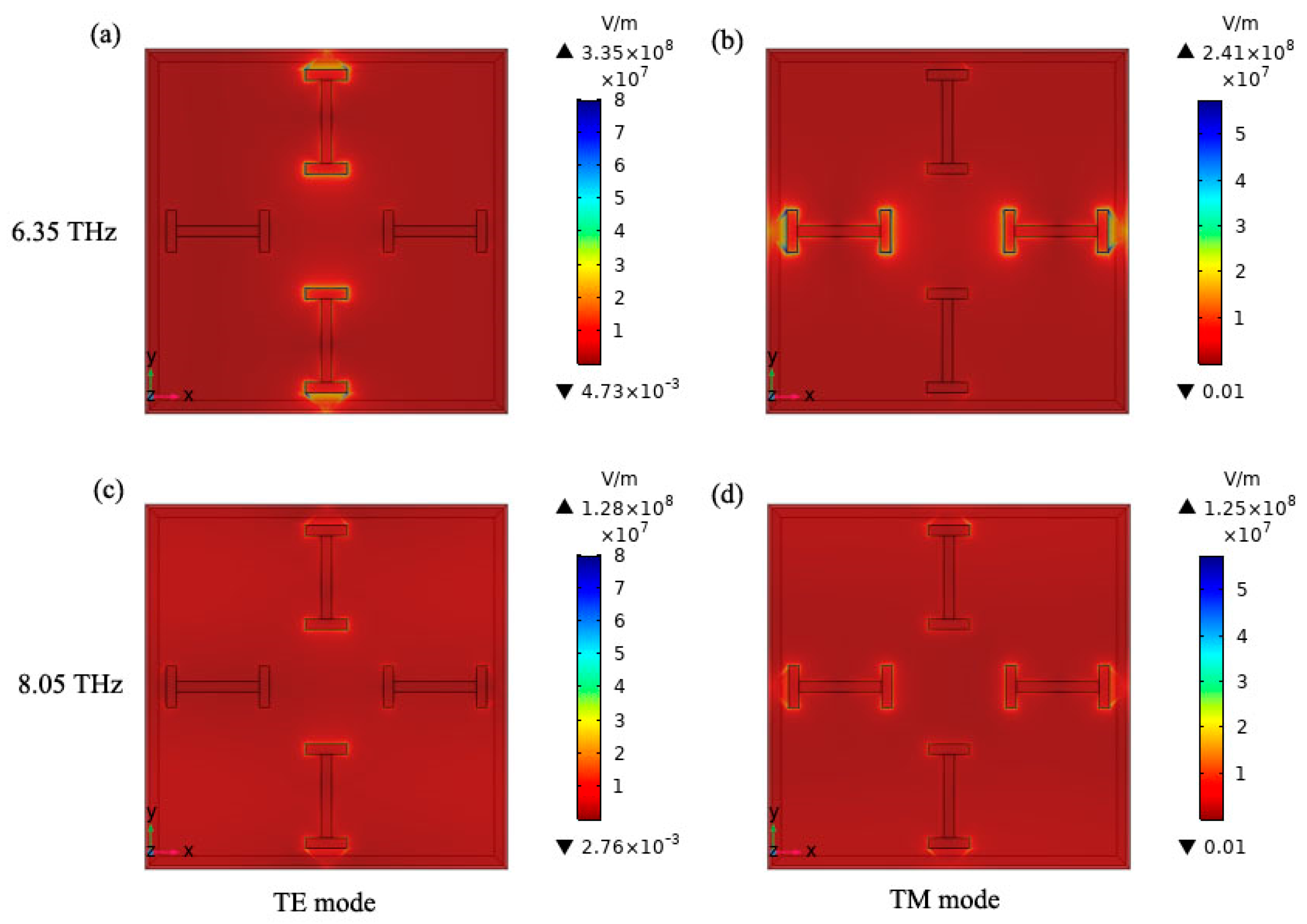
3.1. Absorptivity of Electric and Magnetic Field

Figure 2a,b shows the absorption spectra of the TE-polarized and TM-polarized states, respectively. TE mode refers to a propagation mode, in which the longitudinal component of the electric field is zero, and the longitudinal component of the magnetic field is not zero. Similarly, TM mode refers to a propagation mode, in which the longitudinal component of the magnetic field is zero, and the longitudinal component of the electric field is not zero. In this simulation, the incident electromagnetic wave propagates along the z-axis, and the thickness of the metal absorber layer is h b = 0.03   μ m . We can find two absorption peaks for the two polarization states, with resonance frequencies of 6.35 THz and 8.05 THz, where the electric and magnetic fields have absorption peaks in excess of 99% at 6.35 THz, and the magnetic field has a weaker absorption peak at 8.05 THz. This is due to the fact that few materials exist in nature with negative magnetic permeability. Especially when the frequency exceeds terahertz, the magnetic response of materials in nature becomes weak. This is, mainly, because the magnetic polarization of magnetic materials is derived from either orbital spin or electron spin, but both of these are only responsive to electromagnetic waves in the low-frequency range. At high frequencies, the vast majority of materials have a magnetic permeability of 1 and show no response to the magnetic field component of the electromagnetic wave [34,35,36,37]. With the metamaterial structure, we achieve a strong magnetic response at 6.35 THz and a weaker magnetic response at 8.05 THz, due to the higher frequency, resulting in a weaker magnetic field absorption at 8.05 THz.
Figure 3a–d shows the electric and magnetic field distributions at 6.35 THz and 8.05 THz. The entire metal absorber structure produces electromagnetic resonances in the TE and TM polarization directions, respectively. For the electrical resonance, all metal-tuned structures produce a current in the direction of the electric field. For the magnetic resonance, the entire structure generates a toroidal loop current [38]. The isotropic currents generated in these metal band structures, with the direction of the electric field, affect the surrounding metal bands, thus generating additional coupling capacitance and, in this way, absorbing [39,40,41,42]. With two positive electric field resonances in the TE polarization direction, the TM polarization direction has approximately the same field distribution as the TE polarization direction. From the simulation results, the weak resonation of the electromagnetic field at 8.05 THz can be observed. When the incident light enters the metamaterial structure, the electromagnetic field is completely absorbed, based on the fact that the electromagnetic field is reflected and transmitted many times on the dividing surface of the metamaterial as well as, finally, superimposed many times within the incident surface. If the superimposed result is zero or very small, it means that the electromagnetic field forms an interference phase extinction within the incident surface, after passing through the metamaterial, i.e., no reflection or very small reflection, since the back side is metal, and the electromagnetic field cannot pass through. In addition, when the frequency is higher, the wavelength is shorter, the length of propagation above the partition interface is shorter and the amount of superposition is less, thus, the tutor absorption is weaker. Therefore, the absorption peak at 8.05 THz is much narrower than the peak at 6.35 THz. In conclusion, this I-shaped absorber structure allows for multi-band absorption, and the periodic arrangement of this structure allows for a multi-band absorber to be realized.

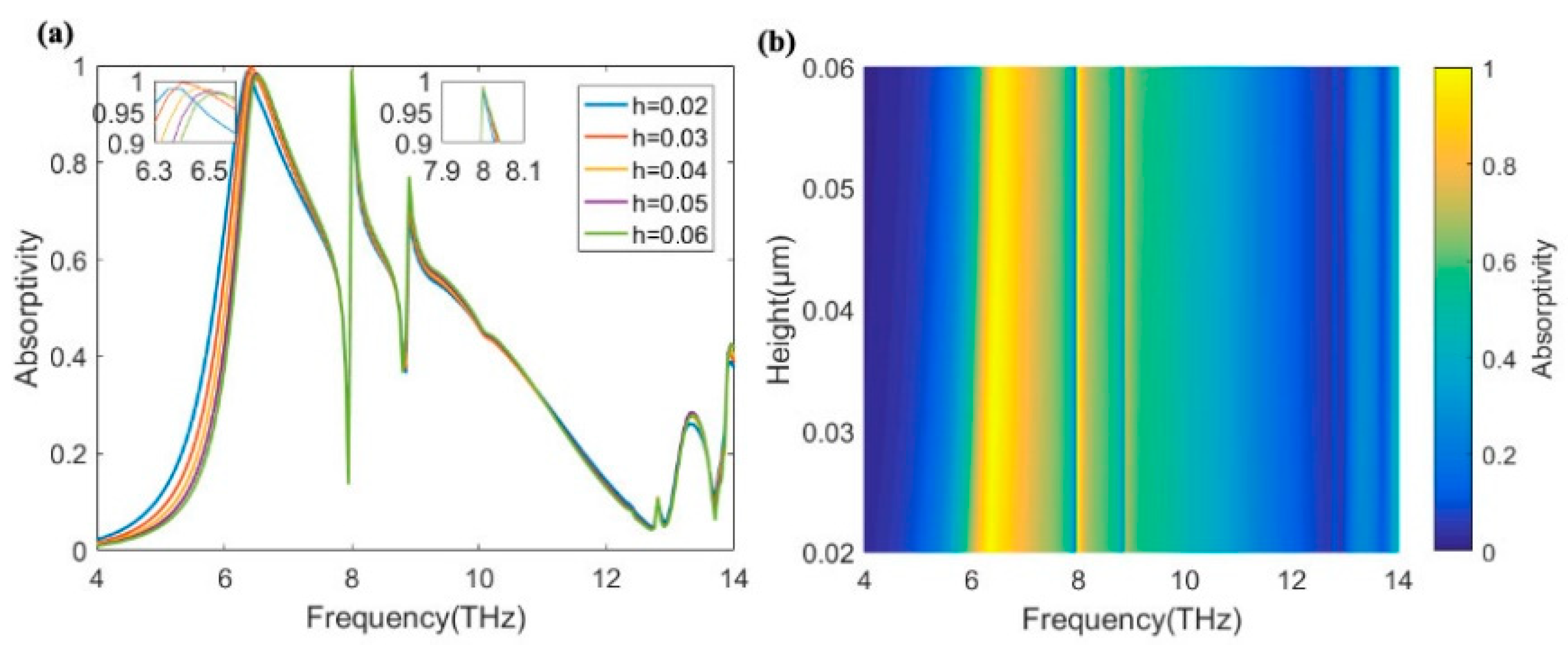
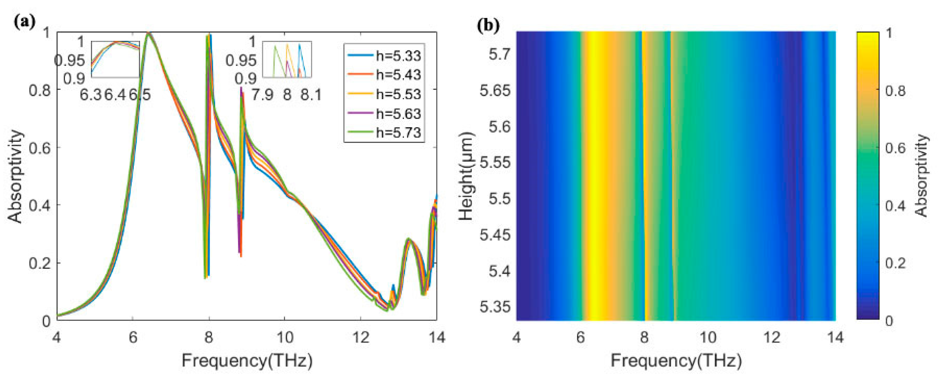
3.2. Absorptivity with the Impact of Thickness of Absorber Layer

Next, we have studied the pattern of influence between the absorbance of the material and the metal absorbing layer, since the thickness of the metal absorber significantly affects the interaction between the near fields. Therefore, in order to obtain a high absorption rate, we adjust the nature of resonant absorption, by modifying the thickness of the metal absorber layer h b and choosing the absorber-layer thickness that corresponds to the highest absorption rate. As shown in Figure 4, we started with a metal-absorber-layer thickness of 0.02 μ m and ramped it up to 0.06 μm, in steps of 0.01 μ m . We can tell that there are two peaks in this absorption structure. The absorption peak at 6.35 THz is significantly redshifted, as the thickness of the metal absorber layer h b increases. However, the absorption remains high in this band, while remaining largely unchanged at 8.05 THz. At h b = 0.03 μ m , the absorption reaches a maximum of 99.73%. The reason for the significant redshift at 6.35 THz is that the air cavity mode between the metal layers can be seen as a FP resonant cavity:
2 π λ m 2 h R e ( n e f f ) + φ r = 2 π m
where λ m is the resonant wavelength, φ r is the phase shift produced by the reflected sections at the ends of the rectangular cavity and m is a positive integer indicating the number of resonance levels [43,44,45,46,47]. The incident electromagnetic field is partly absorbed by the metal wires at the ends of the gas cavity and partly enters the dielectric layer. However, the electromagnetic field entering the dielectric layer cannot be scattered along the interface or through the metal layer, so the resonant peaks are, also, absorbed well.

3.3. Absorptivity with the Impact of Thickness of Dielectric Layer

Next, we researched the relationship between the thickness of the SiO2 layer and the absorption effect of the structure. As shown in Figure 5, the dielectric-layer thickness increased from 5.33 μ m , in steps of 0.1 μ m , to 5.73 μ m . It can be seen the absorption peaks at 6.35 THz are above 99% for different thicknesses of the structure. The absorption peak at 8.05 THz only reaches 99% at dielectric thicknesses of 5.33 μ m and 5.53 μ m , with a significant red shift. The redshift phenomenon can be explained by the propagation phase equation as follows [47,48,49,50,51]:
α = 4 h ε r s i n 2 θ λ
where α is the propagation phase, h is the height of the SiO2 and ε r is the real part of the dielectric constant of this absorbing structure. θ is the angle of incidence and λ is the terahertz wavelength. In the equation, ε r and θ are known values, so, if we assume that α is also a known value, we can conclude that h/λ is known, which means that h is negatively related to the resonant frequency. Thus, as the thickness of SiO2 increases, the peak shifts towards lower frequencies.

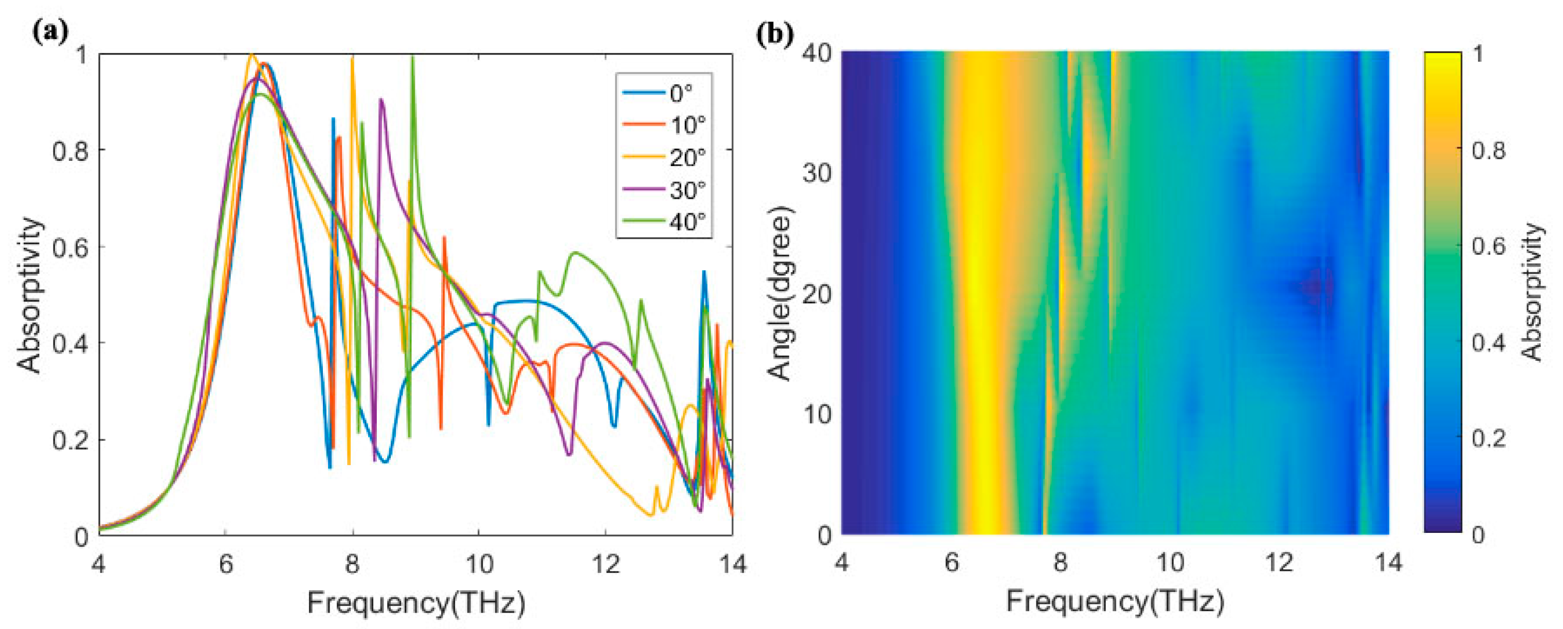
3.4. Absorptivity with the Impact of Incident Angle

Afterwards, we investigated the law of influence, between the angle of incidence and the absorbance of the structure. Absorption spectral lines and scanning absorption patterns were plotted at 4–14 THz, as shown in Figure 6a,b. With the analysis of the patterns, it is obvious that the effect on the change in angle of reception is much bigger. When the angle of incidence is less than 20°, the absorption can exceed 90% of the absorption peak at 6.35 THz. In addition, the absorption effect decreases with an increasing angle. At the beginning, there is an increase in absorption with an increasing angle. Later, as the incidence angle increases, the magnetic dipole oscillations are efficiently excited throughout the absorber. This characteristic maintains acceptable absorptivity at large angles [52,53]. Overall, the absorption is still good at angles of less than 40°.

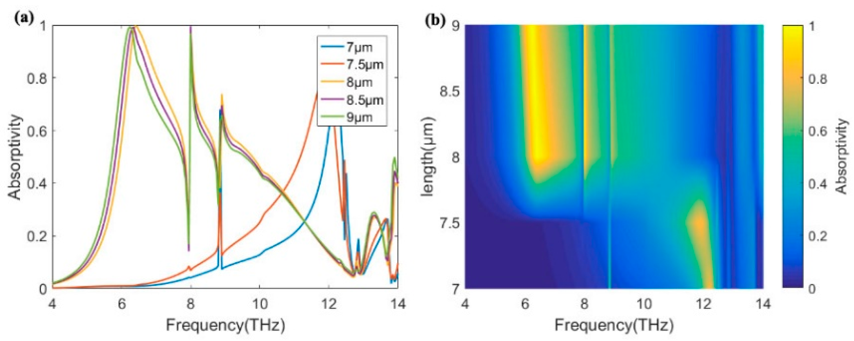
3.5. Absorptivity with the Impact of Length of Metal Structure

Finally, we investigated the relationship between the length of the metal structure in the metal-absorber layer and the absorption rate of the structure. In Figure 7, when the transverse length of the type I structure is less than 8 μm, the absorbing structure has almost no absorption at 6.35 THz and just under 10% absorption at 8.05 THz. This is due to the large spacing between the two sides of the metal structure, which does not enable effective binding of the electromagnetic waves [54,55]. As the metal structure increases, when it increases to 7–9 μ m , the absorbing structure produces a significant absorption peak at two locations, and the absorption rate exceeds 99% This is because, as the length of the metal structure increases, the distance between the different structures draws closer, and the air between them strongly resonates, resulting in two significant absorption peaks.

4. Conclusions

In summary, the structure of perfect absorber has been investigated in the THz region, in consideration of the thickness of the absorber layer, dielectric layer, angle of the incident waves and length of the metal structure. The results indicate that the absorber structure can realize high-level absorption at 6.35 THz and 8.05 THz. By changing the thickness and length of the structure, a perfect absorber has been designed, with 99% absorption at 6.35 THz and 8.05 THz. Therefore, the structure can be effectively used for detectors, thermal emitters, terahertz imaging and detection.

Author Contributions

Z.G.: conceptualization, formal analysis, investigation, data curation, writing–original draft, writing–review and editing; Y.L. (Yanxiu Liu): conceptualization, formal analysis, revision; Y.L. (Ye Li): conceptualization, formal analysis, investigation; P.Z.: conceptualization, formal analysis, revision; Y.Z.: conceptualization, formal analysis, investigation, data curation, revision; S.J.: conceptualization, formal analysis, revision. All authors have read and agreed to the published version of the manuscript.

Funding

This research received no external funding.

Institutional Review Board Statement

Not applicable.

Informed Consent Statement

Not applicable.

Data Availability Statement

Not applicable.

Conflicts of Interest

The authors declare no conflict of interest.

References

  1. Zhou, F.; Qin, F.; Yi, Z.; Yao, W.T.; Liu, Z.M.; Wu, X.W.; Wu, P.H. Ultra-wideband and wide-angle perfect solar energy absorber based on Ti nanorings surface plasmon resonance. Phys. Chem. Chem. Phys. 2021, 23, 17041–17048. [Google Scholar] [CrossRef]
  2. Chen, J.; Guo, J.; Chen, L.Y. Super-wideband perfect solar light absorbers using titanium and silicon dioxide thin-film cascade optical nanocavities. Opt. Mater. Express 2016, 6, 3804–3813. [Google Scholar] [CrossRef]
  3. Chen, J.; Tang, F.; Wang, X.; Wu, J.; Wu, Y.; Ye, X.; Yang, L. High efficiency broadband near-infrared absorbers based on tunable SiO2-VO2-MoS2 multilayer metamaterials. Results Phys. 2021, 26, 104404. [Google Scholar] [CrossRef]
  4. Quidant, R.; Ren, B.; Sailor, M.J. Virtual issue on plasmonic-based sensing. ACS Photonics 2017, 4, 2382–2384. [Google Scholar] [CrossRef]
  5. Li, J.; Liu, B.; Shen, S. Tunable narrow-band near-field thermal emitters based on resonant metamaterials. Phys. Rev. B 2017, 96, 075413. [Google Scholar] [CrossRef] [Green Version]
  6. Shi, C.; Mahlmeister, N.H.; Luxmoore, I.J.; Nash, G.R. Metamaterial-based graphene thermal emitter. Nano Res. 2018, 11, 3567–3573. [Google Scholar] [CrossRef] [Green Version]
  7. Ahi, K. Mathematical modeling of THz point spread function and simulation of THz imaging systems. IEEE Trans. Terahertz Sci. Technol. 2017, 7, 747–754. [Google Scholar] [CrossRef]
  8. Carranza, I.E.; Grant, J.P.; Gough, J.; Cumming, D. Terahertz metamaterial absorbers implemented in CMOS technology for imaging applications: Scaling to large format focal plane arrays. IEEE J. Sel. Top. Quant. 2016, 23, 1–8. [Google Scholar] [CrossRef] [Green Version]
  9. Landy, N.I.; Sajuyigbe, S.; Mock, J.J.; Smith, D.R.; Padilla, W.J. Perfect metamaterial absorber. Phys. Rev. Lett. 2008, 100, 207402. [Google Scholar] [CrossRef]
  10. Fang, Z.; Zhen, Y.R.; Fan, L.; Zhu, X.; Nordlander, P. Tunable wide-angle plasmonic perfect absorber at visible frequencies. Phys. Rev. B 2012, 85, 245401. [Google Scholar] [CrossRef]
  11. Liang, C.; Yi, Z.; Chen, X.; Tang, Y.; Yi, Y.; Zhou, Z.; Zhang, G. Dual-band infrared perfect absorber based on a Ag-dielectric-Ag multilayer films with nanoring grooves arrays. Plasmonics 2020, 15, 93–100. [Google Scholar] [CrossRef]
  12. Shen, X.; Yang, Y.; Zang, Y.; Gu, J.; Han, J.; Zhang, W.; Jun Cui, T. Triple-band terahertz metamaterial absorber: Design, experiment, and physical interpretation. Appl. Phys. Lett. 2012, 101, 154102. [Google Scholar] [CrossRef]
  13. Nielsen, M.G.; Pors, A.; Albrektsen, O.; Bozhevolnyi, S.I. Efficient absorption of visible radiation by gap plasmon resonators. Opt. Express 2012, 20, 13311–13319. [Google Scholar] [CrossRef] [PubMed] [Green Version]
  14. Zhang, X.; Lin, Y.S. Actively electromagnetic modulation of IHI-shaped terahertz metamaterial with high-efficiency switching characteristic. Results Phys. 2019, 15, 102532. [Google Scholar] [CrossRef]
  15. Qin, F.; Chen, Z.; Chen, X.; Yi, Z.; Yao, W.; Duan, T.; Yi, Y. A tunable triple-band near-infrared metamaterial absorber based on Au nano-cuboids array. Nanomaterials 2020, 10, 207. [Google Scholar] [CrossRef] [Green Version]
  16. Ogawa, S.; Fujisawa, D.; Kimata, M. Theoretical investigation of all-metal-based mushroom plasmonic metamaterial absorbers at infrared wavelengths. Opt. Eng. 2015, 54, 127104. [Google Scholar] [CrossRef] [Green Version]
  17. Wei, B.; Jian, S. A near-infrared perfect absorber assisted by tungsten-covered ridges. Plasmonics 2019, 14, 179–185. [Google Scholar] [CrossRef]
  18. Wang, B.X.; Tang, C.; Niu, Q.; He, Y.; Chen, T. Design of narrow discrete distances of dual-/triple-band terahertz metamaterial absorbers. Nanoscale Res. Lett. 2019, 14, 64. [Google Scholar] [CrossRef] [Green Version]
  19. Princy, S.; Sreeja, B.S.; Manikandan, E.; Radha, S. Design of polarisation-dependent multiband terahertz frequency-selective surface using two resonators. Pramana 2019, 92, 1–5. [Google Scholar] [CrossRef]
  20. Barzegar-Parizi, S. Graphene-based tunable dual-band absorbers by ribbon/disk array. Opt. Quant. Electron. 2019, 51, 167. [Google Scholar] [CrossRef] [Green Version]
  21. Huang, L.; Chowdhury, D.R.; Ramani, S.; Reiten, M.T.; Luo, S.N.; Taylor, A.J.; Chen, H.T. Experimental demonstration of terahertz metamaterial absorbers with a broad and flat high absorption band. Opt. Lett. 2012, 37, 154–156. [Google Scholar] [CrossRef] [PubMed] [Green Version]
  22. Mou, N.; Tang, B.; Li, J.; Dong, H.; Zhang, L. Switchable ultra-broadband terahertz wave absorption with VO2-based metasurface. Sci. Rep. 2022, 12, 2051. [Google Scholar] [CrossRef] [PubMed]
  23. Huang, M.; Wei, K.; Wu, P.; Xu, D.; Xu, Y. Terahertz Broadband Absorber Based on a Combined Circular Disc Structure. Micromachines 2021, 12, 1290. [Google Scholar] [CrossRef] [PubMed]
  24. Kong, X.R.; Dao, R.N.; Zhang, H.F. A tunable double-decker ultra-broadband THz absorber based on a phase change material. Plasmonics 2019, 14, 1233–1241. [Google Scholar] [CrossRef]
  25. Liu, Y. Design and measure of a tunable reflection polarization converter based on hybrid dielectric layer metamaterials. J. Mater. Sci. Mater. Electron. 2019, 30, 7175–7181. [Google Scholar] [CrossRef]
  26. Wang, X.; Liang, Y.; Wu, L.; Guo, J.; Dai, X.; Xiang, Y. Multi-channel perfect absorber based on a one-dimensional topological photonic crystal heterostructure with graphene. Opt. Lett. 2018, 43, 4256–4259. [Google Scholar] [CrossRef]
  27. Kassa-Baghdouche, L. Optical properties of a point-defect nanocavity-based elliptical-hole photonic crystal for mid-infrared liquid sensing. Phys. Scr. 2019, 95, 015502. [Google Scholar] [CrossRef]
  28. Kassa-Baghdouche, L.; Boumaza, T.; Bouchemat, M. Optimization of Q-factor in nonlinear planar photonic crystal nanocavity incorporating hybrid silicon/polymer material. Phys. Scr. 2015, 90, 065504. [Google Scholar] [CrossRef]
  29. Duan, M.; Wu, J.; Zhang, Y.; Zhang, N.; Chen, J.; Lei, Z.; Ye, X. Ultra-Low-Reflective, Self-Cleaning Surface by Fabrication Dual-Scale Hierarchical Optical Structures on Silicon. Coatings 2021, 11, 1541. [Google Scholar] [CrossRef]
  30. Li, Z.; Yi, Z.; Liu, T.; Liu, L.; Chen, X.; Zheng, F.; Yan, P. Three-band perfect absorber with high refractive index sensing based on an active tunable Dirac semimetal. Phys. Chem. Chem. Phys. 2021, 23, 17374–17381. [Google Scholar] [CrossRef]
  31. Chen, P.; Liu, F.; Ding, H.; Chen, S.; Chen, L.; Li, Y.J.; Yin, S.F. Porous double-shell CdS@ C3N4 octahedron derived by in situ supramolecular self-assembly for enhanced photocatalytic activity. Appl. Catal. B Environ. 2019, 252, 33–40. [Google Scholar] [CrossRef]
  32. Li, J.; Jiang, J.; Xu, Z.; Liu, M.; Tang, S.; Yang, C.; Qian, D. Facile synthesis of Ag@ Cu2O heterogeneous nanocrystals decorated N-doped reduced graphene oxide with enhanced electrocatalytic activity for ultrasensitive detection of H2O2. Sens. Actuators B Chem. 2018, 260, 529–540. [Google Scholar] [CrossRef]
  33. Xiao, L.; Youji, L.; Feitai, C.; Peng, X.; Ming, L. Facile synthesis of mesoporous titanium dioxide doped by Ag-coated graphene with enhanced visible-light photocatalytic performance for methylene blue degradation. RSC Adv. 2017, 7, 25314–25324. [Google Scholar] [CrossRef] [Green Version]
  34. Veselago, V.G. The electrodynamics of substances with simultaneously negative values of img align= absmiddle Alt= ϵ Eps/Img and μ. Physics-Uspekhi 1968, 10, 509–514. [Google Scholar] [CrossRef]
  35. Smith, D.R.; Kroll, N. Negative refractive index in left-handed materials. Phys. Rev. Lett. 2000, 85, 2933. [Google Scholar] [CrossRef] [Green Version]
  36. Lu, J.; Grzegorczyk, T.M.; Zhang, Y.; Pacheco Jr, J.; Wu, B.I.; Kong, J.A.; Chen, M. Čerenkov radiation in materials with negative permittivity and permeability. Opt. Express 2003, 11, 723–734. [Google Scholar] [CrossRef]
  37. Kumara, K.; Kindalkar, V.S.; Serrao, F.J.; Shetty, T.C.S.; Patil, P.S.; Dharmaprakash, S.M. Enhanced nonlinear optical absorption in defect enriched graphene oxide and reduced graphene oxide using continuous wave laser z-scan technique. Mater. Today 2022, 55, 186–193. [Google Scholar] [CrossRef]
  38. Ye, Y.Q.; Jin, Y.; He, S. Omnidirectional, polarization-insensitive and broadband thin absorber in the terahertz regime. JOSA B 2010, 27, 498–504. [Google Scholar] [CrossRef]
  39. Zhou, J.; Economon, E.N.; Koschny, T.; Soukoulis, C.M. Unifying approach to left-handed material design. Opt. Lett. 2006, 31, 3620–3622. [Google Scholar] [CrossRef]
  40. Xu, L.; Zeng, J.; Luo, X.; Xia, L.; Ma, Z.; Peng, B.; Wang, L. Dual-band plasmonic perfect absorber based on the hybrid halide perovskite in the communication regime. Coatings 2021, 11, 67. [Google Scholar] [CrossRef]
  41. Tanaka, T.; Ishikawa, A. Towards three-dimensional optical metamaterials. Nano Converg. 2017, 4, 34. [Google Scholar] [CrossRef] [PubMed] [Green Version]
  42. Liu, N.; Guo, H.; Fu, L.; Kaiser, S.; Schweizer, H.; Giessen, H. Plasmon hybridization in stacked cut-wire metamaterials. Adv. Mater. 2007, 19, 3628–3632. [Google Scholar] [CrossRef]
  43. Zhang, Q.; Huang, X.G.; Lin, X.S.; Tao, J.; Jin, X.P. A subwavelength coupler-type MIM optical filter. Opt. Express 2009, 17, 7549–7554. [Google Scholar] [CrossRef]
  44. Boltasseva, A.; Bozhevolnyi, S.I.; Nikolajsen, T.; Leosson, K. Compact Bragg gratings for long-range surface plasmon polaritons. J. Light. Technol. 2006, 24, 912. [Google Scholar] [CrossRef]
  45. Zhao, H.; Guang, X.G.; Huang, J. Novel optical directional coupler based on surface plasmon polaritons. Phys. E 2008, 40, 3025–3029. [Google Scholar] [CrossRef]
  46. Han, Z.; Forsberg, E.; He, S. Surface plasmon Bragg gratings formed in metal-insulator-metal waveguides. IEEE Photonic Technol. Lett. 2007, 19, 91–93. [Google Scholar] [CrossRef]
  47. Dionne, J.A.; Sweatlock, L.A.; Atwater, H.A.; Polman, A.J.P.R.B. Plasmon slot waveguides: Towards chip-scale propagation with subwavelength-scale localization. Phys. Rev. B 2006, 73, 035407. [Google Scholar] [CrossRef] [Green Version]
  48. Lu, X.; Wan, R.; Zhang, T. Metal-dielectric-metal based narrow band absorber for sensing applications. Opt. Express 2015, 23, 29842–29847. [Google Scholar] [CrossRef]
  49. Yao, T.; Wei, C.W.; Simpson, R.E.; Zhang, L.; Cryan, M.J. Broadband polarization-independent perfect absorber using a phase-change metamaterial at visible frequencies. Sci. Rep. 2014, 4, 3955. [Google Scholar] [CrossRef]
  50. Tian, X.; Li, Z.Y. Visible-near infrared ultra-broadband polarization-independent metamaterial perfect absorber involving phase-change materials. Photonics Res. 2016, 4, 146–152. [Google Scholar] [CrossRef]
  51. Li, Q.; Gao, J.; Yang, H.; Liu, H.; Wang, X.; Li, Z.; Guo, X. Tunable plasmonic absorber based on propagating and localized surface plasmons using metal-dielectric-metal structure. Plasmonics 2017, 12, 1037–1043. [Google Scholar] [CrossRef]
  52. Ma, X.; Xu, X.; Zheng, Z.; Wang, K.; Su, Y.; Fan, J.; Zhu, J. Dynamically modulated intensity interrogation scheme using waveguide coupled surface plasmon resonance sensors. Sens. Actuators A Phys. 2010, 157, 9–14. [Google Scholar] [CrossRef]
  53. Colomban, P. The use of metal nanoparticles to produce yellow, red and iridescent colour, from bronze age to present times in lustre pottery and glass: Solid state chemistry, spectroscopy and nanostructure. J. Nano Res. 2009, 8, 109–132. [Google Scholar] [CrossRef] [Green Version]
  54. Yu, N.; Aieta, F.; Genevet, P.; Kats, M.A.; Gaburro, Z.; Capasso, F. A broadband, background-free quarter-wave plate based on plasmonic metasurfaces. Nano Lett. 2012, 12, 6328–6333. [Google Scholar] [CrossRef]
  55. Grady, N.K.; Heyes, J.E.; Chowdhury, D.R.; Zeng, Y.; Reiten, M.T.; Azad, A.K.; Chen, H.T. Terahertz metamaterials for linear polarization conversion and anomalous refraction. Science 2013, 340, 1304–1307. [Google Scholar] [CrossRef] [Green Version]
Figure 1. (a) Absorber simulation structure. (b) Schematic diagram of the main structure of the absorber. (c) Cross-sectional structure of the absorber layer.
Coatings 12 00687 g001
Figure 2. Electric and magnetic field distributions in (a) TE and (b) TM modes.
Coatings 12 00687 g002
Figure 3. (a) Electric field distribution at 6.35 THz in TE polarization mode. (b) Magnetic field distribution at 6.35 THz in TM polarization mode. (c) Electric field distribution at 8.05 THz in TE polarization mode. (d) Magnetic field distribution at 8.05 THz in TM polarization mode.
Coatings 12 00687 g003
Figure 4. (a) Absorption curves corresponding to different metal-absorber-layer thicknesses. (b) Absorption rate trends with absorber-layer height, corresponding to different metal-absorber-layer thicknesses.
Coatings 12 00687 g004
Figure 5. (a) Absorbance curves corresponding to different dielectric-layer thicknesses. (b) Trend of absorbance with dielectric layer height corresponding to different dielectric-layer thicknesses.
Coatings 12 00687 g005
Figure 6. (a) Absorption rate curves corresponding to different angles. (b) Trend of absorption rate corresponding to different angles.
Coatings 12 00687 g006
Figure 7. (a) Absorbance curves for different metal-structure lengths. (b) Absorption rate trend for different metal-structure lengths.
Coatings 12 00687 g007
Table 1. Related research overview.
Manuscript AuthorAbsorption PeakAbsorption
Wei et al.670 nm, 957 nmOver 90%
Wang, B.X. et al.2.06 THz, 2.27 THz, 2.51 THzAbout 100%
Princy et al.0.078 THz, 0.142 THz, 0.39 THz, 0.47 THzAbout 100%
Barzegar-Parizi1.2 THz, 2.7 THzAbout 100%
Huang, L. et al.0.905 THz, 0.956 THz99.9%
Mou, N.L. et al.0.398~1.356 THzOver 90%
Huang, M.H. et al.8.62~10 THzOver 97%
Kong, X.R. et al.7.12~8.39 THz, 10.29~13.59 THz, 15.1~18.12 THzOver 90%
Liu, Y.1.61~2.42 THzAverage 94.2%
Publisher’s Note: MDPI stays neutral with regard to jurisdictional claims in published maps and institutional affiliations.

