Review

Infrared-to-Visible Upconversion Devices

1
School of Optics and Photonics, Beijing Institute of Technology, Beijing 100081, China
2
Beijing Key Laboratory for Precision Optoelectronic Measurement Instrument and Technology, Beijing Institute of Technology, Beijing 100081, China
3
Yangtze Delta Region Academy, Beijing Institute of Technology, Jiaxing 314019, China
*
Authors to whom correspondence should be addressed.
Coatings 2022, 12(4), 456; https://doi.org/10.3390/coatings12040456
Submission received: 28 February 2022 / Revised: 23 March 2022 / Accepted: 24 March 2022 / Published: 27 March 2022
(This article belongs to the Special Issue Application of Advanced Quantum Dots Films in Optoelectronics)

Abstract

:
Infrared imaging plays remarkable roles in various fields including military, biomedicine, aerospace, and artificial intelligence. However, traditional infrared imaging systems have plenty of disadvantages such as large volume, high cost, and complex fabrication process. Emerging infrared upconversion imaging devices can directly convert low-energy infrared photons into high-energy visible light photons, thus they are promising to accomplish pixel-less high-resolution infrared imaging at low cost. In this paper, recent advances and progress of infrared-to-visible upconversion devices are summarized. We further offer the main limitations of upconversion technology and the challenges that need to be addressed for the future development of infrared upconverters.

1. Introduction

Human vision is limited in the visible wavelength range of 400 to 700 nm. The detection and visualization of electromagnetic waves with wavelengths beyond the range of human vision, such as visualization of near-infrared (NIR), short-wave infrared (SWIR), or mid-infrared (MIR) light, is of vital importance and challenging. Optical sensing and imaging devices in the NIR have a wide range of applications in communications [1], bio-imaging [2], machine vision systems, non-invasive subsurface vision, night vision [3,4], optical sensors for semiconductor inspection, and non-contact industrial and consumer electronic displays. SWIR with wavelengths ranging from 1.5 to 3 μm covers the second and third biological windows. SWIR photodetection and visualization in this wavelength range plays an essential role in numerous applications [5,6,7] such as environmental pollution, environmental monitoring, bio-imaging, medicine, agriculture, automobiles, food, health monitoring, etc. These applications are due to SWIR’s unique properties, for example, reducing light scattering and absorption key role, deeply penetrating into biological tissues, and reducing phototoxicity. MIR refers to 3–5 μm-band infrared, which belongs to the “atmosphere window”, that is, there are many infrared radiation transmission components from the atmosphere. Therefore, an MIR detector [8,9,10] plays an important role in atmospheric monitoring, gas detection, infrared countermeasures, and other aspects. At the same time, MIR has great research value in the field of military infrared detection, especially infrared thermal imaging [11,12,13] and infrared guidance.
Infrared imaging systems contain objective information that cannot be reflected by visible light imaging and have indispensable applications in many fields such as military, aerospace, remote sensing mapping, autonomous driving, astronomical science, medical, health care, and others. Focusing on the new generation of cutting-edge application scenarios and demands such as unmanned aerial vehicles, mobile reconnaissance, and smart cities in the future, infrared imaging has become the focus of current research.
However, up to now, the most mature infrared imaging technology is the traditional infrared focal plane imaging technology. This imaging technology mainly has the following two problems: (1) the interconnection of the detector and the readout circuit needs to grow tens of thousands of indium pillars and complete it through the flip-chip interconnection process, which is not only complicated and expensive, but also unreliable; (2) the output electric signal not only needs to be read out by the readout circuit but the imaging processing circuit is also very complicated. It can be seen that the preparation technology of infrared materials and the conversion processing of photoelectric signals have become the core problems that limit the development of infrared imaging technology.
In response to the above challenges, a new type of photonic upconverter called infrared-to-visible upconversion device has emerged. The upconverter can convert invisible infrared images to visible light without pixelated processing in the device. In contrast to traditional infrared imaging technology, upconversion devices convert low-energy incident infrared photons into high-energy output visible light photons, which are then imaged by commercial visible light imaging technology or directly observed by the naked eyes. Currently, there are primarily two upconversion mechanisms: nonlinear optical processes and linear optical processes.
Nonlinear upconversion is the synthesis of infrared light and visible light into a new beam of visible light whose frequency is the sum of the two (sum frequency process). This kind of upconversion device is directly realized by upconversion luminescent materials. Triplet–triplet annihilation (TTA)-based near-infrared to visible molecular photon upconversion [14,15,16,17,18,19,20,21,22] and nanoparticle-based upconversion [23,24,25,26] are two main upconversion luminescent materials. Early achievements on infrared upconversion are mainly based on Ge/GaAs heterojunction structures and rare-earth ion doping systems. There are two representative works. Yoh Mita demonstrated an infrared-excitable phosphor-based upconverter that can detect 1.5 µm NIR and has visible or NIR emissions [27]. Yuhu Wang et al., in 1993, proposed a device whose upconversion situation has been observed with Er3+-doped BaCl2 phosphors [28]. From these nonlinear upconversions mentioned above, the conclusion that can be drawn is that those materials need two or more photons, and then through nonradiative relaxation the photons reach the luminescence level, transition to the ground state, and emit a visible photon. With the purpose of realizing high-efficiency infrared light upconversion, it is necessary for the propagation among infrared light, visible light, and upconverted light to meet the conditions of mutual matching. This nonlinear process based on momentum matching often involves complicated and difficult optical path and material design and usually requires an expensive high-power pulsed light source to emit visible light, which is unfavorable to its wider application.
Therefore, an infrared-to-visible upconversion device based on linear photon upconversion is an ideal scheme to realize high-performance, low-cost infrared imaging. Its working principle is that by integrating infrared photodetectors (PD) that absorb infrared photons and the light-emitting diodes (LED) that excite visible photons together, the low-energy infrared light can be converted into high-energy visible light by using the linear conversion process of light–electricity–light, thus realizing infrared detection and imaging. This infrared upconversion imaging method has many advantages. Firstly, there is no need to pixelize the large-area imaging device and interconnect and align indium pillars for each pixel by a flip-chip bonding process, which greatly simplifies the process. Secondly, visible light images can be directly observed with the naked eye without complicated readout circuits and signal processing processes, and infrared imaging can be realized by using efficient visible light imaging technologies such as CCD cameras, which can significantly improve imaging efficiency, resolution, and sensitivity; Thirdly, in the later stage, there is no need to carry out complicated pseudo-color-coding processing on the image. The pseudo-color images, which are more sensitive for the naked eye, can be directly realized from hardware, for the multi-color LED that can produce the color change is coupled with the infrared detector.
Based on the difference in semiconductor materials of PD and LED units, in this article, the type of optical upconverters can be divided into four categories: all-inorganic upconversion devices, all-organic upconversion devices, inorganic semiconductor infrared detector and organic LED (OLED) hybrid optical upconverter (hybrid organic–inorganic upconversion devices) and colloidal quantum dots-based upconversion devices. According to the different infrared bands detected by the four kinds of upconverters, they are discussed separately. Progress in upconversion devices is summarized in Figure 1.

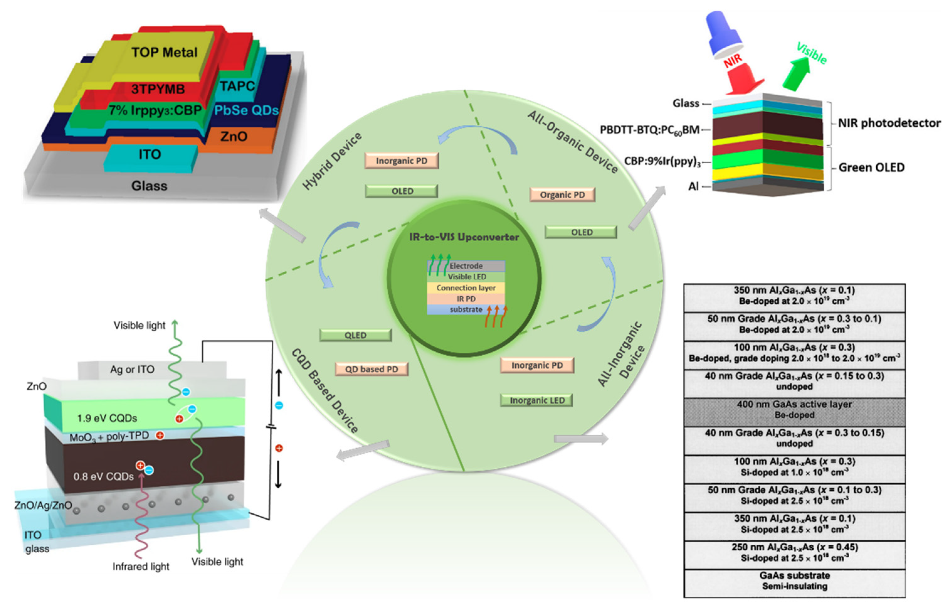
2. Types of Upconversion Device

Compared with traditional infrared imaging technology, infrared upconversion devices have obvious advantages in reducing production cost, simplifying the manufacturing process, improving imaging resolution and sensitivity, reducing the size and weight of the imaging system, etc., and have shown excellent performance in the field of infrared imaging. There have been many reports on infrared upconversion devices both domestically and abroad.

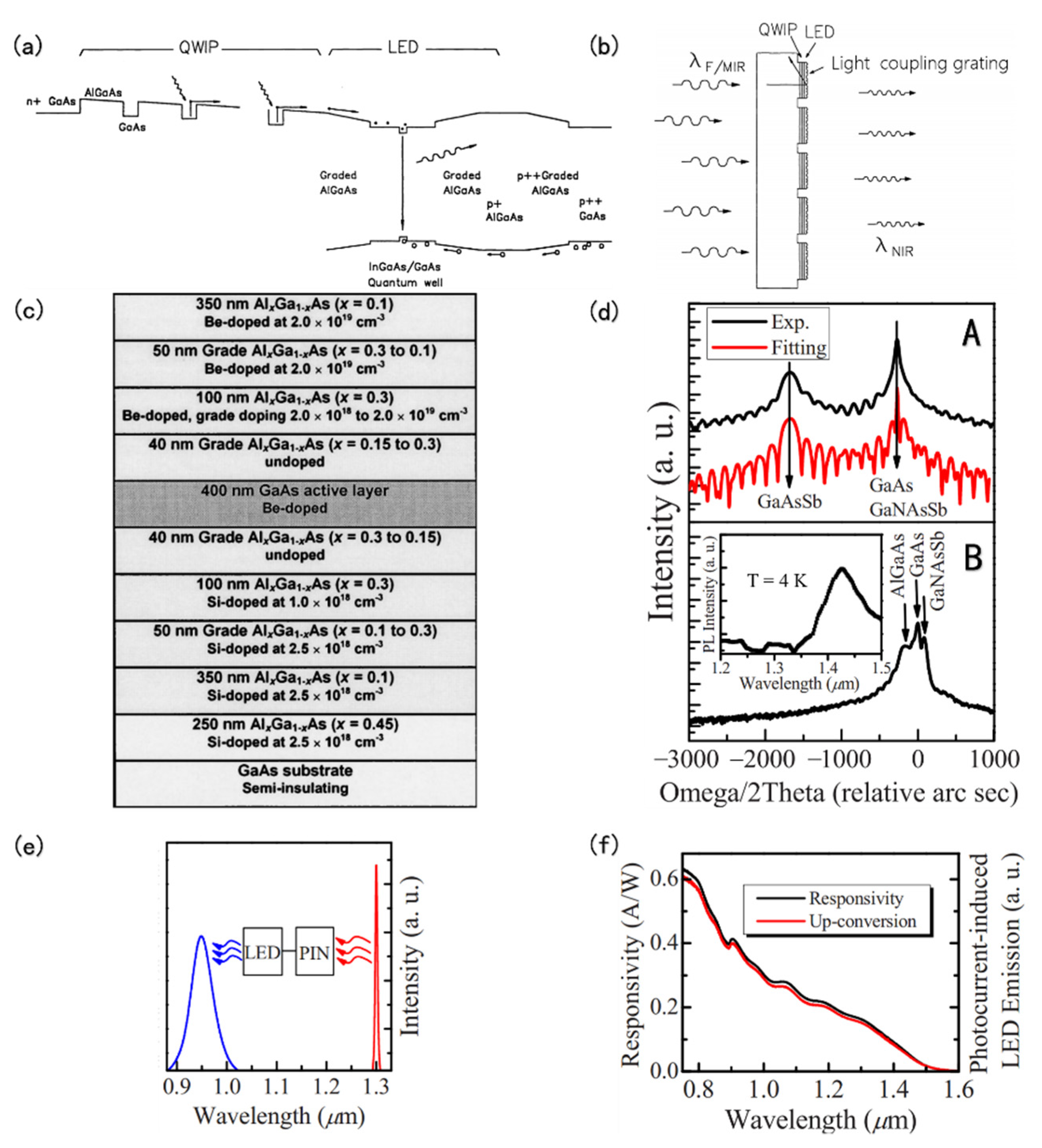
2.1. All-Inorganic Upconversion Devices

In 1995, HC Liu successfully used epitaxial growth technology to connect quantum well infrared detectors (GaAs/AlGaAs) and LEDs in series, and integrated inorganic upconversion devices (Figure 2a,b), which realized infrared upconversion imaging from NIR of ~1.5 μm to shorter wavelengths (~0.9 μm) for the first time [29]. In 2000, Liu et al., proposed a mechanism for upconversion using semiconductor structures. InGaA/InP PD and InAsP/InP light-emitting diodes (LED) were grown on InP substrates to prepare room temperature NIR upconverters. However, the upconversion efficiency was less than 0.0005 W/W due to the energy barrier limiting quantum efficiency within the LED and poor carrier constraints in the InAsP/InP LEDs active region [30].
In 2004, to address the mismatch between the GaAs substrate and the active layer lattice of the GaAs detector, which increases rapidly with the increase of indium content, InGaAs/InP PD and GaAs/AlGaAs LED were combined by wafer fusion (Figure 2c). This processing technique was used to integrate heterogeneous semiconductor materials regardless of their lattice mismatch. The results show that this method is effective and improves the efficiency of the upconversion (~0.018 W/W) [31]. However, for pure inorganic upconverter, even if the upconverter is integrated by wafer fusion technology, the cost of epitaxial growth cannot be further reduced, and the ideal conversion efficiency cannot be obtained. Based on a similar structure, in 2009, Shanghai Jiaotong University reported an inorganic upconversion device integrated with GaAsSb/GaAs PD and GaAs/AlGaAs LED (Figure 2d–f), which upconverted NIR light of about 1.3 μm to about 0.95 μm NIR light, with an upconversion efficiency of 4.8% [32].
However, due to the very large energy band difference between LED and infrared photodetection materials, the device can only achieve upconversion from longer wavelengths to shorter wavelengths in the infrared range, not visible light. In addition, the epitaxial growth of traditional upconverters requires very high lattice parameter matching.

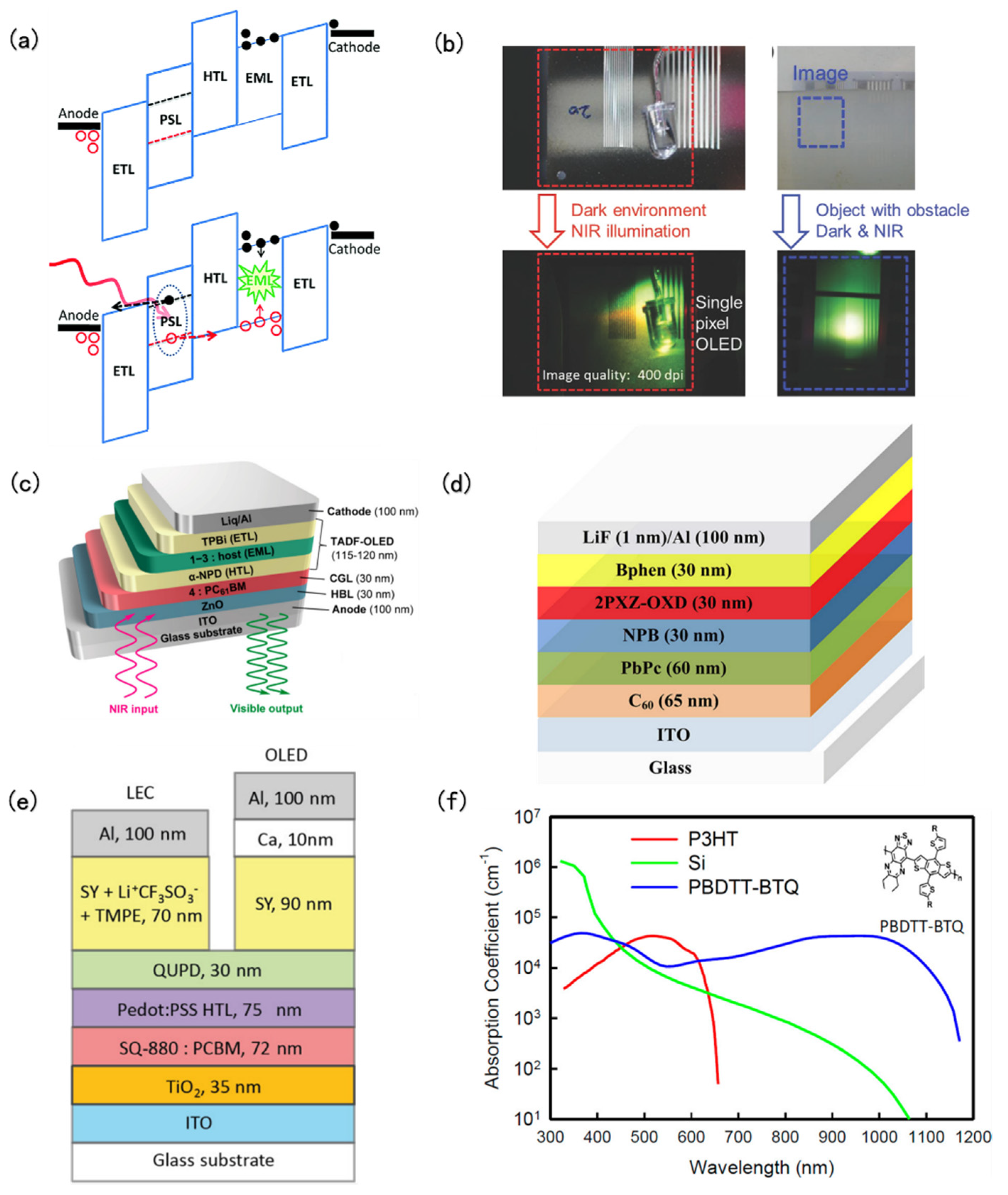
2.2. All-Organic Upconversion Devices

Organic electronic devices are expected to be applied to infrared upconversion devices to realize upconversion in the visible light band due to the no lattice matching growth requirements of organic materials. Besides, organic materials are independent of the properties of the substrate material and can be deposited on any material with a low production cost.
All-organic upconverters were first reported on the basis of fluorescent LEDs, which consist of an organic PD sensitive to the infrared and an OLED connected in series. In addition, OLEDs can work at ultra-low temperatures, which ensures that they can work normally when integrated with other detectors in any infrared band. All-organic upconverters promise multiple advantages of organic electronics, and they also provide the possibility of converting NIR scenes into visible images by using large-area devices. These devices can be implemented on flexible substrates at low cost, simplifying the manufacturing process, reducing the production cost, and are currently a commonly used infrared-to-visible light upconversion device.

2.2.1. NIR-to-Visible Upconversion

In 2007, Lu et al. firstly proposed an all-organic upconversion device using 2,4,7-trinitro-9-flfluorenylidene malonitrile (TNFDM) as an infrared photosensitive material, which realized the upconversion process of the visible light emission intensity changing with the incident infrared power and confirmed the feasibility of all-organic NIR–visible light upconversion device [33]. In 2010, Kim et al. prepared an all-organic upconversion device with a conversion efficiency of 2.7% by using SnPc:C60 as an infrared detection material and a phosphorescent material with a higher external quantum efficiency than fluorescent materials as a luminescent material [34]. In 2018, D. Yang et al. proposed the concept of using tandem OLED (Figure 3a) that integrates an NIR polymer PD and a green tandem OLED together to fabricate organic upconversion devices, for the use of two layers of light-emitting. The injected electron–hole pairs can be more efficiently converted into visible light than those devices that only have one layer. In this work, they reach one of the highest peak photon-to-photon conversion efficiency up to 29.6% at that time [35]. S. Liu and co-workers, in 2015, demonstrated a transparent upconverter, the NIR light can be converted into visible light with the upconversion device. Moreover, this work is the first one that demonstrated night vision by using a reflective and nonreflective object (Figure 3b) [36].
OLEDs can already achieve the emission of the three primary colors of red, green, and blue, so through the fusion of the three primary colors, they can achieve display in the full visible range. According to the full-color OLED, in 2017, Tachibana et al. reported high-performance all-organic full-color upconversion devices (Figure 3c). They used thermally activated delayed fluorescence (TADF) for the first time. Their result has great potential for NIR imaging applications with large area, low cost, and pixel-less imaging [37].
Upconversion efficiency is vital to upconversion devices. Many attempts have been made in order to improve the photon-to-photon upconversion efficiency. In 2018, Song and his co-workers promoted integrating a photo multiplying organic NIR PD with a high-efficiency TADF-OLED (Figure 3d), and through this method, the photon-to-photon upconversion efficiency can run up to 256% [38].
In these cases cited above, there is no more than 900 nm NIR light upconverted to visible light. In 2018, Strassel and his co-workers extended the NIR spectral peak sensitivity up to 1000 nm, meanwhile, this device is visibly transparent and the innovative use of NIR selective squaraine dye is the highlight of this work [41]. In 2019, the same team reported a solution-processed upconversion device, by adding an electrolyte to the super yellow (SY) emitter (Figure 3e), thereby transforming the OLED into a light-emitting electrochemical cell (LEC), which is more fault-tolerant and has a lower driving voltage than traditional OLED [39]. In the same year, Yeddu et al. raised infrared sensitivity up to 1.1 μm. For such long-wavelength infrared light detection, the detector requires low bandgap organic semiconductors, therefore, they synthesized a novel low bandgap polymer poly 4-(4,8-bis (5-(2-butyloctyl) thiophen-2-yl) benzo [1,2-b:4,5-b′] dithiophen-2-yl)-6,7-diethyl- [1,2,5] thiadiazol [3,4-g] quinoxaline (PBDTT-BTQ) with strong photoresponse in NIR wavelengths of 700−1100 nm which the previously used Si-based PDs cannot offer. PBDTT-BTQ’s infrared absorption is superior to others as shown in Figure 3f [40].

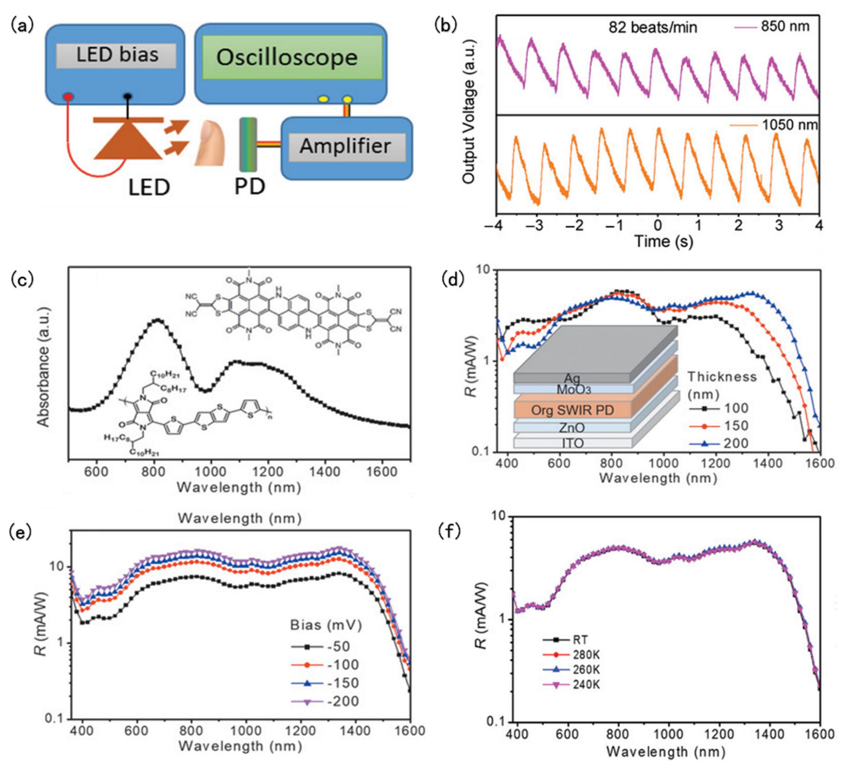
2.2.2. SWIR-to-Visible Upconversion

In 2020, Li and his co-workers reported their efforts in all solution-based process SWIR-to-visible upconversion devices. They fabricated a blend of a diketopyrrolopyrrole–dithienylthieno[3,2-b] thiophene (DPP–DTT) polymer donor and a hetero-polycyclic aromatic compound SWIR dye with a CsPbBr3 perovskite LED. This device can detect infrared light up to 1400 nm and convert it to 516 nm visible green light [42]. The spectral detection of hybrid upconverters is expanded to the SWIR range for the first time. This advanced device can be operated without cooling and was proved to apply in biological fields, such as providing reliable heart rate monitoring. The structure and performance of this upconverter are shown in Figure 4.
In summary, the infrared-to-visible upconversion devices have developed from the traditional all-inorganic structure to the widely used all-organic structure at present, successfully achieving low-cost infrared-to-visible light upconversion imaging. However, for almost every all-organic upconversion device only the NIR band can be detected, and the upconversion efficiency of the device is very low. Generally, it can only work under the high-power infrared laser, which cannot meet the requirements of practical application.

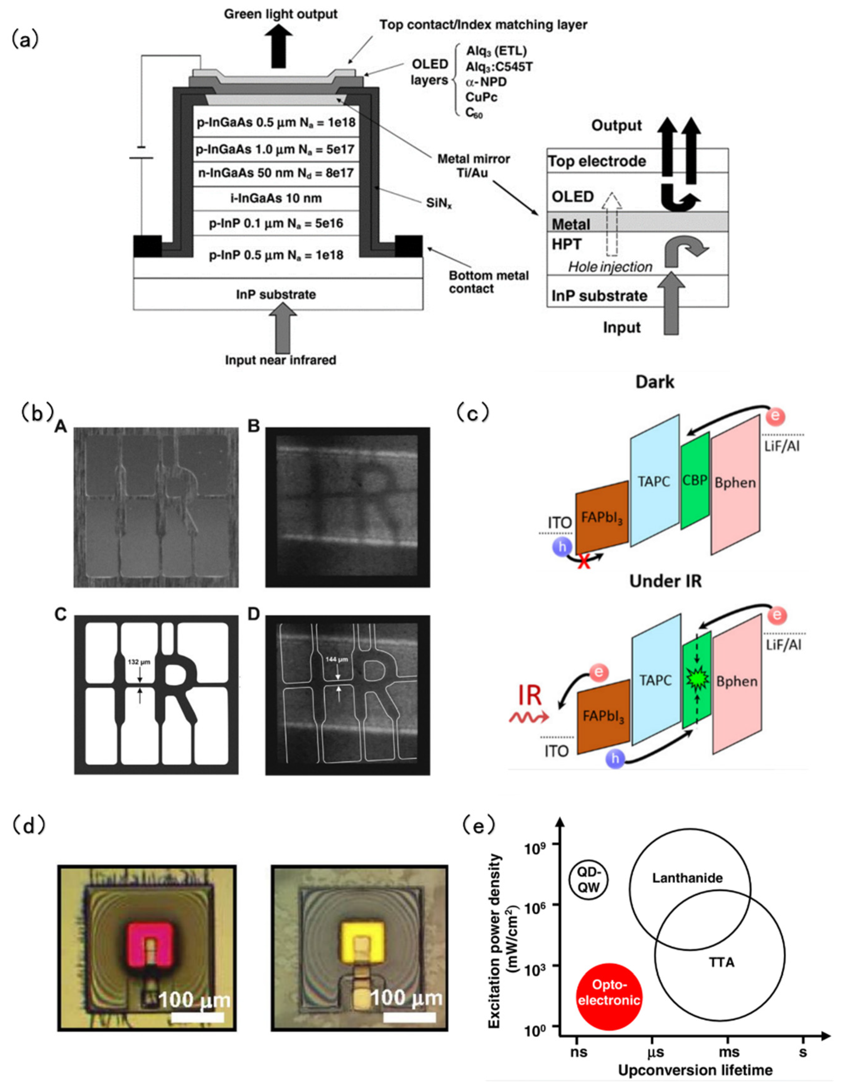
2.3. Hybrid Organic–Inorganic Upconversion Devices

Previously, blended organic and inorganic materials were synthesized and manufactured to form devices. The flexibility of organic chemistry allows organic molecules to form with useful luminescent and conducting properties. Due to the stronger covalent and ionic bonds, inorganic materials can be designed to have better thermal/mechanical stability and higher electromigration. Using different emissive organic materials, the wavelengths of OLED emissions can vary across the full visible spectrum. However, inefficient photo carrier injection from inorganic detectors to OLEDs results in low infrared-to-visible upconversion efficiency. Therefore, there is still a lot of work for researchers to do in order to enhance devices’ performance.

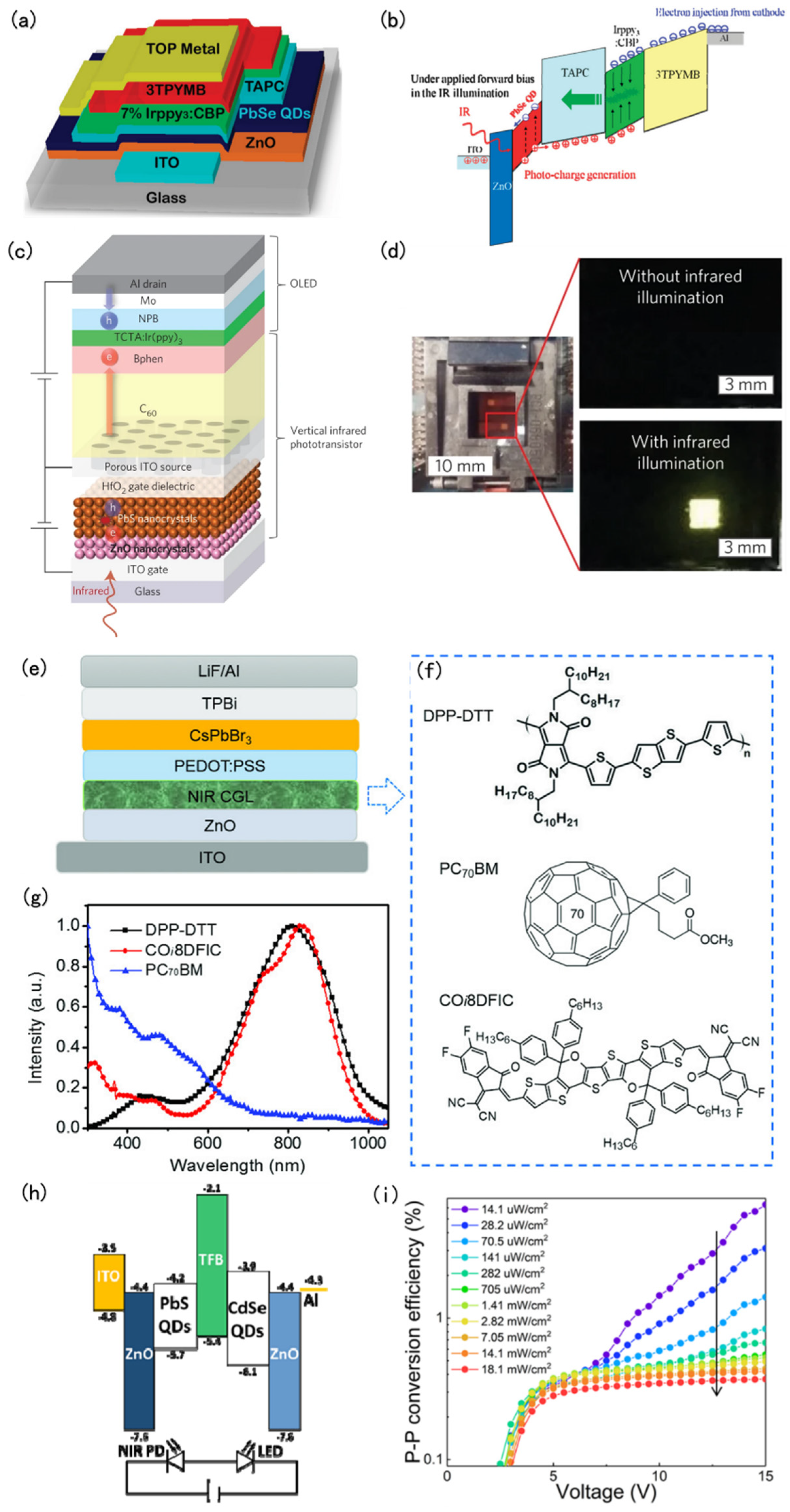
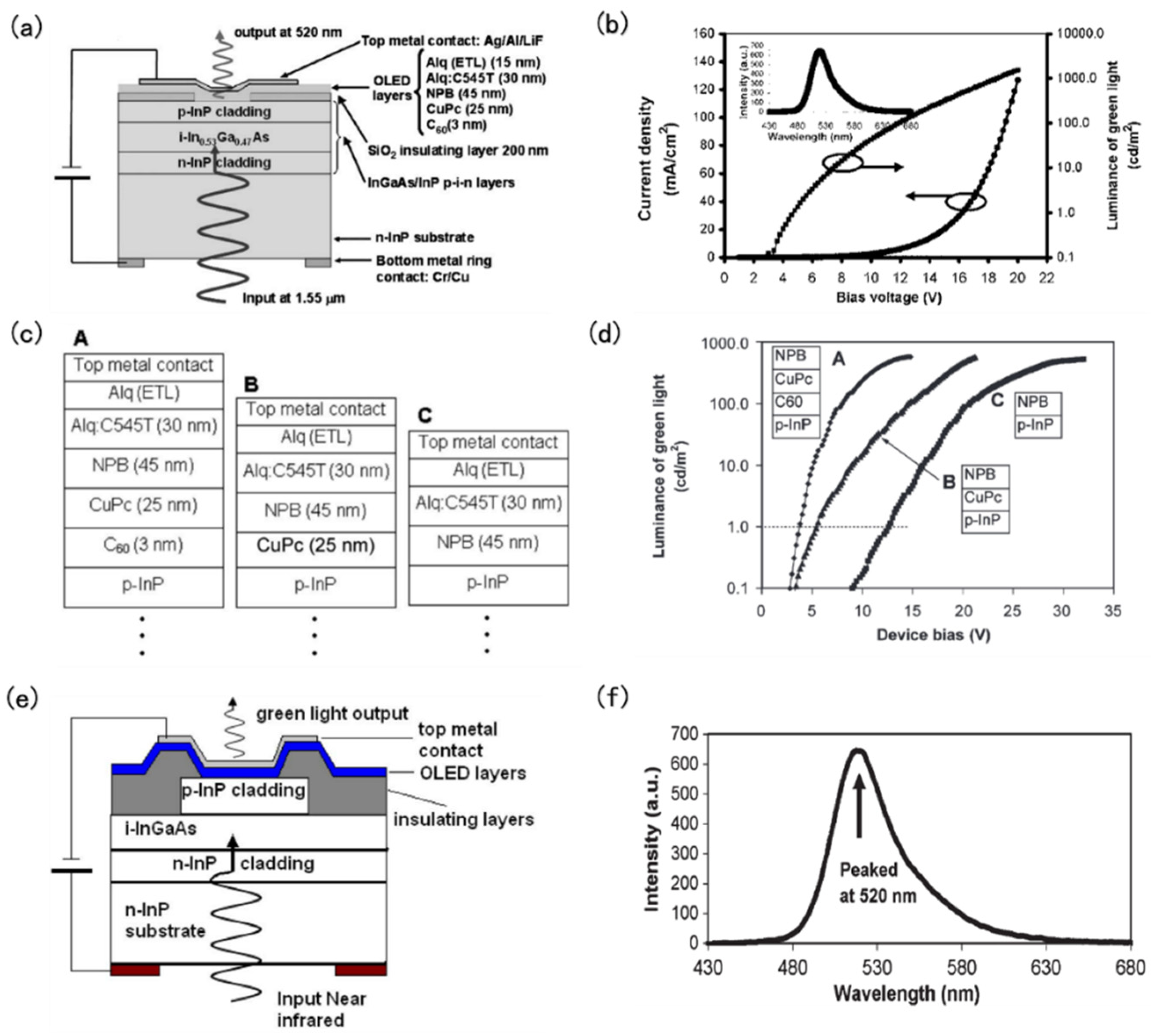
2.3.1. NIR-to-Visible Upconversion

In 2008, Chen et al., of the University of Waterloo, added a Ti/Au thin film between the InGaAs infrared detector and the OLED, and the conversion efficiency of the integrated upconversion device was improved to 1.5% [43]. Based on this research, in 2010, Chen et al. obtained an optical upconverter by optimizing the structure of an InGaAs/InP heterojunction phototransistor (HPT) with a gain mechanism and integrating it with an OLED [44]. The structure and equivalent circuit diagram of this upconverter are shown in Figure 5a. The optical upconverter not only realizes the conversion of 1.5 µm NIR to green light (520 nm) at room temperature but also achieves the optical power conversion efficiency of 1.55 W/W (corresponding to an external quantum efficiency of 59%).
In 2012, Chen et al., proposed a pixel-less imaging upconversion device, they employed Technology Computer-Aided Design software (TCAD) to simulate the propagation of photo-generated hole carriers in the upconverter, it was found that no matter how large the size of the incident infrared beam is, the concentration distribution of photo-generated holes at the intermediate interface of i-InGaAs/C60 shows that the lateral propagation distance is less than 1 µm [45]. The NIR-to-visible light upconverter was used for pixel-less imaging. The image displayed under the NIR illumination through the shaped hole and the characteristic length of the shaped hole and the image are shown in Figure 5b. From the image they demonstrated, the actual resolution of the device can be calculated. The resulting spatial resolution of 6 µm is smaller than its calculated theoretical value of 1 µm. According to their analysis, the small resolution was mainly due to the limited resolution of digital cameras (~6 µm). However, the infrared pixel-less imaging device achieved a spatial resolution better than 6 µm, which was sufficient for practical applications.
Generally, due to the serial device architecture, the turn-on voltage of the upconversion devices is high. In 2018, Yu et al. reported a low turn-on voltage upconverter, the photocarrier can be efficiently injected into the OLED from the perovskite layer under NIR light, due to the perovskite layer supplied extra voltage to activate the OLED at a 1.9 eV sub-band voltage. On this account, the upconversion device lights up at 1.9 V [46], which is lower than the bandwidth voltage of the emitting layer in the OLED. Further on, Yu et al. demonstrated the pixel-free NIR imaging at a low operation voltage of 3 V which is shown in Figure 5c.
In the same year, Ding et al. reported an NIR-to-visible upconversion strategy based on fully integrated microscale optoelectronic devices, and the dimension of this device is 220 μm × 220 μm (Figure 5d). These devices were implanted in behaving animals, and their effectiveness in photogenetic nerve regulation was proved by in vitro and in vivo experiments. They proposed the theory of the photon–“free electron”–photon process eliminating the limitation of traditional nonlinear upconversion methods [47]. In 2019, Shi et al. reported an ultrafast and low-power optoelectronic NIR-to-visible upconversion device, similar to Ding’s theory, they applied the photo–“free electron”–photon concept. Their devices can be excited at low power (1–100 mW/cm2) and the devices’ luminescence decay lifetime (Figure 5e) can be adjusted from ~20 to ~200 ns. Such unique characteristic is beneficial for the application of high-flow chemical detection and dynamic biological stimulations [48].

2.3.2. SWIR-to-Visible Upconversion

In 2007, Ban et al. took the lead in proposing an organic–inorganic hybrid upconversion device integrating in series with an InGaAs/InP infrared detector and an OLED and successfully upconverted SWIR light of 1.55 μm that can be converted into green visible light of 520 nm. However, the conversion efficiency of this infrared-to-visible upconversion device is only 0.7% [49]. The structure and performance of this upconverter are shown in Figure 6a,b.
For an OLED device, its structure is generally composed of an anode, hole injection layer (HIL), hole transport layer (HTL), emission layer, electron transport layer (ETL), electron injection layer (EIL), and cathode. Obviously, in addition to the light-emitting layer, other parts will also affect the performance of the device. Ban et al. also compared the effects of different HTL layer structures on the device performance as shown in Figure 6c. The HTL layer of device C has only one layer of N, N′-di(naphthalene-l-yl)-N, N′-diphenyl-benzidine (NPB), device B adds a layer of CuPc under NPB, and device A continues to add a layer of C60 under CuPc [50]. It can be seen from Figure 6d that the organic–inorganic interface has a great influence on the efficient injection of holes, and the turn-on voltage of device C is different from that of devices A and B, because the addition of C60 can reduce the carrier injection barrier. The structure and emission spectrum of this upconverter are shown in Figure 6e,f.

2.4. Colloidal Quantum Dots-Based Upconversion Devices

From what was discussed above, most all-organic and hybrid upconversion devices can only convert NIR light into visible light, but usually cannot detect short-wave infrared light, and the application range is severely limited. Besides, the upconversion efficiency of the device is very low [29,37,40,41,42,45,49], for these organic–inorganic upconversion devices, which are limited by the low photon–electron conversion efficiency of the infrared PD part. Generally, infrared-to-visible upconversion devices can only work under the high-power infrared laser, which cannot meet the practical application requirements. Most of the reported infrared upconversion devices need to be fabricated by high-cost vacuum deposition methods [35,37,45,46], and as for inorganic infrared detectors in hybrid upconversion devices, they still need to be fabricated by epitaxial growth, both of these two problems make the fabrication cost of organic–inorganic hybrid upconversion devices still expensive and unsuitable for large-area imaging applications. In addition, the reported infrared upconversion devices have high operating voltages, which are not conducive to the preparation of flexible devices.
Quantum dots (QDs) have narrow emission linewidth and adjustable bandgap, so that tunable infrared response can be realized in a wide spectral range, and it is the reason that QDs have great potential value in developing quantum information and opto-electronic devices. For example, bulk mercury telluride (HgTe) materials are semi-metallic materials with zero bandgap and large exciton Bohr radii. With the help of the “quantum confinement effect”, HgTe QDs [8,9,10,51,52,53,54,55,56] can theoretically achieve full spectrum coverage in the infrared to terahertz range. Therefore, the application of colloidal QDs (CQDs), in the field of infrared detectors can realize infrared detection in all major infrared bands of NIR, SWIR, and MIR. In addition, the luminescence spectrum of CQDs is extremely narrow, the color saturation and purity are high, and the optical stability is very good, which can be synthesized in a large-scale liquid phase. Therefore, quantum dot LEDs (QLEDs) have excellent performances of a wide color gamut, long life, and low cost.
CQDs, in particular, can be synthesized by solution treatment, and used in photovoltaics, luminescence, and photodetection. Except for the top electrode, the entire infrared upconversion device is prepared by solution method, which greatly simplifies the preparation of the device. Therefore, the infrared upconversion devices based on CQDs, benefiting from the property of CQDs, can be processed by solution method and can be fabricated into flexible devices.

2.4.1. NIR-to-Visible Upconversion

In 2011, Kim and his co-workers reported their achievement of a low-cost upconversion device with infrared sensitivity up to 1.5 μm using PbSe inorganic colloidal nanocrystals as infrared PD. It was the first time that the NIR-to-visible light converter of CQDs’ integrated phosphorescent emitting OLED was reported, the structure and schematic diagram are shown in Figure 7a,b. It must be known that all-organic upconversion devices before this work nearly had no infrared sensitivity beyond 1 μm, moreover, there were not any hybrid devices that could reach a 1.3% photon-to-photon conversion efficiency (that this work obtained) in the past. In contrast to previous studies, Kim et al. employed a wide bandgap ZnO layer as a hole blocking layer to improve the on/off ratio of the device, and the dark current of the device was obviously reduced, moreover the signal-to-noise ratio of the device was increased [57].
In 2016, Yu et al. reported a novel upconversion light-emitting phototransistor (LEPT) by incorporating a phosphorescent OLED into a phototransistor. To be different from the ascending upconverters with two terminals, this LEPT is a vertical three-terminal phototransistor with an infrared photoactive gate integrated into an OLED, which has high-efficiency such as its external quantum efficiency (EQE) of up to 1 × 10⁵% and detectivity of 1.23 × 10¹³ Jones [58]. The structure of this LEPT is demonstrated in Figure 7c, and a photograph of the sample clamped in the measurement box is shown in Figure 7d. In 2018, Li et al. demonstrated a perovskite LED based on CsPbBr3 with high performance, it can be processed in solution and has a narrow emission spectrum. Their research proved that the NIR-sensitive polymer DPP–DTT blend with a norfullerene acceptor COi8DFIC is an appropriate layer of charge generation layer for the upconversion procession, as a result of its unique combination of high NIR absorption and low visible light absorption (Figure 7e–g) [59]. In 2020, Tang and his co-workers proposed a high conversion efficiency for all QDs-based upconverters (Figure 7h). Former upconversion systems were always manufactured by inorganic semiconductors using wafer fusion technology. However, they were limited by the mismatch of lattice between different semiconductors, leading to poor photonic conversion efficiency. As for the all-organic devices, their efficiency has been improved a lot, but the stability of these upconverters is still a potential issue for their application. In this reference, the use of innately stable, efficient, and high-performance QDs made the device achieve a high photon-to-photon conversion efficiency of 6.3% (Figure 7i), and can be fabricated by solution process [60].

2.4.2. SWIR-to-Visible Upconversion

In 2020, Ning Zhijun’s research group from ShanghaiTech University integrated CQD infrared detectors and colloidal QLED for the first time to obtain a CQD infrared-to-visible light upconversion device (Figure 8a). This all-CQDs upconversion device had high photonic conversion efficiency of up to 6.5%, and it can be turned on at a low applied bias of only 2.5 V. Through this upconverter the short-wave infrared (Figure 8b) with a power density of 10–600 mW·cm−2 was converted into visible green light (520 nm) (Figure 8c). Ning’s group incorporated silver nanoparticles in the PD’s layers that can extract charges (Figure 8d) with the aim of optimizing the carrier tunneling and making the PD layer provide enough photocurrent so that the LED can be turned on successfully. This advanced achievement confirms the application of CQDs in upconversion devices and the feasibility of realizing SWIR upconversion imaging [61].

2.4.3. MIR-to-Visible Upconversion

In 2020, Motmaen reported a novel and high-performance integrated chip which can realize the upconversion process from MIR (3–5 µm) to the green light (523 nm). This upconversion device was fabricated using a doped PbSe layer as a PD, an NPN (n-type, p-type, n-type) bipolar junction transistor (NPN-BJT) as a current amplifier, and an OLED as an emission layer; its structure is shown in Figure 9a, the energy band diagram is shown in Figure 9b. In this new type of upconverter, PbSe QDs were used to realize the photodetection and generate current, then the output electric information can be amplified by NPN-BJT. With the amplified current the LED can be driven and emits visible green light [62]. Under 3 μm MIR light illumination (0.5 mW/cm2) (Figure 9c) and total voltage of 13.5 V, the EQE is calculated to 600% (Figure 9d), such high EQE is mainly thanks to the amplifier function of NPN-BJT.
The liquid semiconductor QDs synthesized by colloidal chemistry can precisely tune the bandgap by adjusting the size, and then achieve tunable infrared photoresponse in a wide spectral range. Therefore, from the above demonstration, it can be seen that the application of CQDs in the field of infrared-to-visible upconversion can realize infrared detection in all main infrared bands of NIR, SWIR, and MIR.
Therefore, after several decades of development, infrared-to-visible upconversion devices have shown a transition trend from traditional all-inorganic, all-organic, and organic–inorganic materials to emerging liquid CQD materials. The development of infrared-to-visible light upconversion devices based on CQDs has become one of the important trends to achieve wide detecting spectrum, high-performance, low-cost, flexible, and large-area infrared imaging in the future. The performance of the upconversion devices in the references discussed above is shown in Table 1.

3. Challenges and Perspectives

Although infrared upconversion devices have made many remarkable signs of progress in the past few years and some advantages of them are irreplaceable, there are still some important problems that need further consideration.
  • The detecting wavelength of infrared-to-visible upconverters is mostly concentrated in the near-infrared range. Although some SWIR and MIR spectral range devices are reported, those upconversion devices still have to improve photon-to-photon conversion efficiency, reduce the turn-on voltage and optimize other performance parameters. The short detection wavelength of upconversion devices limits their application scenarios.
  • The upconversion efficiency and sensitivity of infrared-to-visible light upconversion devices are relatively low. The upconversion efficiency of the currently reported devices is difficult to exceed 10%, leading to most of the existing devices only operating under intense infrared light (usually an infrared incident power range of 10–100 mW cm−2).
  • In many medical and commercial fields, the performance of flexible devices is very important. Even though some all-solution-based processes can be achieved, with these methods the flexible devices’ performance characterization is scarce, meanwhile, the brightness and life time of flexible devices are unsatisfactory.
Overall, the performance of infrared-to-visible upconversion devices remains to be significantly enhanced to meet application requirements. High conversion efficiency, low turn-on voltage, flexible device, and wide detection band are vital to upconverters. To meet these above challenges, we need to pay more attention to the following aspects.
  • Low dimensional materials, such as zero-dimensional materials (CQD), one-dimensional materials (III-Sb nanowires), and two-dimensional materials (quantum well, graphene, and black phosphorus) possess tunable bandgaps, high carrier mobility, precisely controlled materials growth process, low cost, and solution process compatibility, thus they have been widely applied in both infrared detectors and LED fields. In the future, there may be a strong trend of low dimensional materials replacing traditional materials to be utilized in infrared-to-visible upconversion devices.
  • The upconversion efficiency and sensitivity of the infrared-to-visible upconversion device are the keys to determining whether it can detect weak infrared light in nature for practical use. Therefore, the high upconversion efficiency and sensitivity to meet the practical application of upconversion infrared imaging may become important trends in future development.
  • To manufacture a flexible device with stable performance and to characterize it accordingly, it is necessary to optimize and improve the existing manufacturing materials and manufacturing methods of the upconverter. The current flexible devices are based on CQD materials, but these materials are often very toxic and cannot be used in large-scale production applications. Therefore, only flexible devices with high performance and low toxicity can be used in biology and other fields.
  • Broaden the wavelength range of upconversion. In fact, due to the invisible light range from 700 nm to 1100 nm for the naked eye, it can be easily detected by traditional silicon PDs. Thus, it could be said that the benefits of the upconversion device concept only become obvious when NIR light with wavelengths beyond the silicon band can be upconverted into visible light. The current upconversion devices are mainly concentrated in the NIR band, and the research on SWIR and above infrared upconversion devices is much less. Although CQD semiconductor materials have the ability to cover the main wavelength bands of infrared, the maximum infrared detection wavelength (1.6 μm) of all-CQDs-based infrared-to-visible upconversion devices, which just reaches the SWIR and limits its application field. Therefore, it is a mainstream direction for future research and development to break through the infrared detection band range of infrared-to-visible upconversion devices, thereby broadening their application field.

Author Contributions

Conceptualization, X.T., T.R. and G.M.; methodology, M.C.; software, X.T., T.R. and G.M.; validation, X.T., T.R. and G.M.; formal analysis, M.C.; investigation, X.T., T.R. and G.M.; resources, X.T., T.R. and G.M.; data curation, X.T., T.R. and G.M.; writing—original draft preparation, T.R., G.M.; writing—review and editing, X.T.; visualization, X.T., T.R. and G.M.; supervision, X.T.; project administration, X.T.; funding acquisition, X.T. All authors have read and agreed to the published version of the manuscript.

Funding

This research was funded by the National Natural Science Foundation of China and the National Key R&D Program of China (NSFC No. 62035004, 2021YFA0717600, and NSFC No. 62105022).

Institutional Review Board Statement

Not applicable.

Informed Consent Statement

Not applicable.

Data Availability Statement

Not applicable.

Conflicts of Interest

The authors declare no conflict of interest.

References

  1. Minotto, A.; Haigh, P.A.; Łukasiewicz, Ł.G.; Lunedei, E.; Gryko, D.T.; Darwazeh, I.; Cacialli, F. Visible light communication with efficient far-red/near-infrared polymer light-emitting diodes. Light Sci. Appl. 2020, 9, 70. [Google Scholar] [CrossRef] [PubMed] [Green Version]
  2. Kim, S.; Lim, Y.T.; Soltesz, E.G.; De Grand, A.M.; Lee, J.; Nakayama, A.; Parker, J.A.; Mihaljevic, T.; Laurence, R.G.; Dor, D.M.; et al. Near-infrared fluorescent type II quantum dots for sentinel lymph node mapping. Nat. Biotechnol. 2004, 22, 93–97. [Google Scholar] [CrossRef] [PubMed]
  3. Schreiner, K. Night Vision: Infrared takes to the road. IEEE Comput. Graph. Appl. 1999, 19, 6–10. [Google Scholar] [CrossRef]
  4. Bellotti, C.; Bellotti, F.; De Gloria, A.; Andreone, L.; Mariani, M. Developing a near infrared based night vision system. IEEE Intell. Veh. Symp. Proc. 2004, 2004, 686–691. [Google Scholar] [CrossRef]
  5. Chorier, P.; Tribolet, P.M.; Fillon, P.; Manissadjian, A. Application needs and trade-offs for short-wave infrared detectors. Infrared Technol. Appl. XXIX 2003, 5074, 363. [Google Scholar] [CrossRef]
  6. Nelson, M.P.; Shi, L.; Zbur, L.; Priore, R.J.; Treado, P.J. Real-time short-wave infrared hyperspectral conformal imaging sensor for the detection of threat materials. Chem. Biol. Radiol. Nucl. Explos. Sens. XVII 2016, 9824, 982416. [Google Scholar] [CrossRef]
  7. Wang, M.; Knobelspiesse, K.D.; McClain, C.R. Study of the Sea-Viewing Wide Field-of-View Sensor (SeaWiFS) aerosol optical property data over ocean in combination with the ocean color products. J. Geophys. Res. D Atmos. 2005, 110, D10S06. [Google Scholar] [CrossRef] [Green Version]
  8. Keuleyan, S.; Lhuillier, E.; Brajuskovic, V.; Guyot-Sionnest, P. Mid-infrared HgTe colloidal quantum dot photodetectors. Nat. Photonics 2011, 5, 489–493. [Google Scholar] [CrossRef]
  9. Ackerman, M.M.; Tang, X.; Guyot-Sionnest, P. Fast and Sensitive Colloidal Quantum Dot Mid-Wave Infrared Photodetectors. ACS Nano 2018, 12, 7264–7271. [Google Scholar] [CrossRef] [PubMed]
  10. Ackerman, M.M.; Chen, M.; Guyot-Sionnest, P. HgTe colloidal quantum dot photodiodes for extended short-wave infrared detection. Appl. Phys. Lett. 2020, 116, 083502. [Google Scholar] [CrossRef]
  11. Amani, M.; Regan, E.; Bullock, J.; Ahn, G.H.; Javey, A. Mid-Wave Infrared Photoconductors Based on Black Phosphorus-Arsenic Alloys. ACS Nano 2017, 11, 11724–11731. [Google Scholar] [CrossRef] [PubMed]
  12. Hoang, A.M.; Dehzangi, A.; Adhikary, S.; Razeghi, M. High performance bias-selectable three-color Short-wave/Mid-wave/Long-wave Infrared Photodetectors based on Type-II InAs/GaSb/AlSb superlattices. Sci. Rep. 2016, 6, 24144. [Google Scholar] [CrossRef] [PubMed] [Green Version]
  13. Rogalski, A. HgCdTe infrared detector material: History, status and outlook. Rep. Prog. Phys. 2005, 68, 2267–2336. [Google Scholar] [CrossRef] [Green Version]
  14. Nienhaus, L.; Correa-Baena, J.-P.; Wieghold, S.; Einzinger, M.; Lin, T.-A.; Shulenberger, K.E.; Klein, N.D.; Wu, M.; Bulović, V.; Buonassisi, T.; et al. Triplet-Sensitization by Lead Halide Perovskite Thin Films for Near-Infrared-to-Visible Upconversion. ACS Energy Lett. 2019, 4, 888–895. [Google Scholar] [CrossRef]
  15. Wu, M.; Lin, T.-A.; Tiepelt, J.O.; Bulović, V.; Baldo, M.A. Nanocrystal-Sensitized Infrared-to-Visible Upconversion in a Microcavity under Subsolar Flux. Nano Lett. 2021, 21, 1011–1016. [Google Scholar] [CrossRef] [PubMed]
  16. Lissau, J.S.; Khelfallah, M.; Madsen, M. Near-Infrared to Visible Photon Upconversion by Palladium(II) Octabutoxyphthalocyanine and Rubrene in the Solid State. J. Phys. Chem. C 2021, 125, 25643–25650. [Google Scholar] [CrossRef]
  17. Xu, Z.; Huang, Z.; Li, C.; Huang, T.; Evangelista, F.A.; Tang, M.L.; Lian, T. Tuning the Quantum Dot (QD)/Mediator Interface for Optimal Efficiency of QD-Sensitized Near-Infrared-to-Visible Photon Upconversion Systems. ACS Appl. Mater. Interfaces 2020, 12, 36558–36567. [Google Scholar] [CrossRef]
  18. VanOrman, Z.A.; Nienhaus, L. Bulk Metal Halide Perovskites as Triplet Sensitizers: Taking Charge of Upconversion. ACS Energy Lett. 2021, 6, 3686–3694. [Google Scholar] [CrossRef]
  19. Bharmoria, P.; Bildirir, H.; Moth-Poulsen, K. Triplet–triplet annihilation based near infrared to visible molecular photon upconversion. Chem. Soc. Rev. 2020, 49, 6529–6554. [Google Scholar] [CrossRef]
  20. Wu, M.; Congreve, D.N.; Wilson, M.W.B.; Jean, J.; Geva, N.; Welborn, M.; Van Voorhis, T.; Bulović, V.; Bawendi, M.G.; Baldo, M.A. Solid-state infrared-to-visible upconversion sensitized by colloidal nanocrystals. Nat. Photonics 2016, 10, 31–34. [Google Scholar] [CrossRef]
  21. Ye, C.; Zhou, L.; Wang, X.; Liang, Z. Photon upconversion: From two-photon absorption (TPA) to triplet–triplet annihilation (TTA). Phys. Chem. Chem. Phys. 2016, 18, 10818–10835. [Google Scholar] [CrossRef]
  22. Huang, Z.; Xu, Z.; Mahboub, M.; Liang, Z.; Jaimes, P.; Xia, P.; Graham, K.R.; Tang, M.L.; Lian, T. Enhanced Near-Infrared-to-Visible Upconversion by Synthetic Control of PbS Nanocrystal Triplet Photosensitizers. J. Am. Chem. Soc. 2019, 141, 9769–9772. [Google Scholar] [CrossRef] [PubMed]
  23. Liu, Y.; Lu, Y.; Yang, X.; Zheng, X.; Wen, S.; Wang, F.; Vidal, X.; Zhao, J.; Liu, D.; Zhou, Z.; et al. Amplified stimulated emission in upconversion nanoparticles for super-resolution nanoscopy. Nature 2017, 543, 229–233. [Google Scholar] [CrossRef] [PubMed]
  24. Wen, S.; Zhou, J.; Zheng, K.; Bednarkiewicz, A.; Liu, X.; Jin, D. Advances in highly doped upconversion nanoparticles. Nat. Commun. 2018, 9, 2415. [Google Scholar] [CrossRef] [PubMed]
  25. Tao, Y.; Huang, A.J.Y.; Hashimotodani, Y.; Kano, M.; All, A.H.; Tsutsui-kimura, I.; Tanaka, K.F.; Liu, X.; Mchugh, T.J. NIR deep brain stimulation via upconversion nanoparticle-mediated optogenetics. Science 2018, 684, 679–684. [Google Scholar]
  26. Xu, J.; Xu, L.; Wang, C.; Yang, R.; Zhuang, Q.; Han, X.; Dong, Z.; Zhu, W.; Peng, R.; Liu, Z. Near-Infrared-Triggered Photodynamic Therapy with Multitasking Upconversion Nanoparticles in Combination with Checkpoint Blockade for Immunotherapy of Colorectal Cancer. ACS Nano 2017, 11, 4463–4474. [Google Scholar] [CrossRef] [PubMed]
  27. Mita, Y. Detection of 1.5-μm wavelength laser light emission by infrared-excitable phosphors. Appl. Phys. Lett. 1981, 39, 587–589. [Google Scholar] [CrossRef]
  28. Wang, Y.; Ohwaki, J. High-efficiency infrared-to-visible upconversion of Er3+ in BaCl2. J. Appl. Phys. 1993, 74, 1272–1278. [Google Scholar] [CrossRef]
  29. Liu, H.C.; Li, J.; Wasilewski, Z.R.; Buchanan, M. Integrated quantum well intersub-band photodetectorand light emitting diode. Electron. Lett. 1995, 31, 832–833. [Google Scholar] [CrossRef]
  30. Liu, H.C.; Gao, M.; Poole, P.J. 1.5 µm up-conversion device. Electron. Lett. 2000, 36, 1300–1301. [Google Scholar] [CrossRef]
  31. Ban, D.; Luo, H.; Liu, H.C.; Wasilewski, Z.R.; Springthorpe, A.J.; Glew, R.; Buchanan, M. Optimized GaAs/AlGaAs light-emitting diodes and high efficiency wafer-fused optical up-conversion devices. J. Appl. Phys. 2004, 96, 5243–5248. [Google Scholar] [CrossRef]
  32. Yang, Y.; Shen, W.Z.; Liu, H.C.; Laframboise, S.R.; Wicaksono, S.; Yoon, S.F.; Tan, K.H. Near-infrared photon upconversion devices based on GaNAsSb active layer lattice matched to GaAs. Appl. Phys. Lett. 2009, 94, 2007–2010. [Google Scholar] [CrossRef]
  33. Lu, J.; Zheng, Y.; Chen, Z.; Xiao, L.; Gong, Q. Optical upconversion devices based on photosensitizer-doped organic light-emitting diodes. Appl. Phys. Lett. 2007, 91, 201107. [Google Scholar] [CrossRef]
  34. Kim, D.Y.; Song, D.W.; Chopra, N.; De Somer, P.; So, F. Organic infrared upconversion device. Adv. Mater. 2010, 22, 2260–2263. [Google Scholar] [CrossRef] [PubMed]
  35. Yang, D.; Zhou, X.; Ma, D.; Vadim, A.; Ahamad, T.; Alshehri, S.M. Near infrared to visible light organic up-conversion devices with photon-to-photon conversion efficiency approaching 30%. Mater. Horiz. 2018, 5, 874–882. [Google Scholar] [CrossRef]
  36. Liu, S.W.; Lee, C.C.; Yuan, C.H.; Su, W.C.; Lin, S.Y.; Chang, W.C.; Huang, B.Y.; Lin, C.F.; Lee, Y.Z.; Su, T.H.; et al. Transparent organic upconversion devices for near-infrared sensing. Adv. Mater. 2015, 27, 1217–1222. [Google Scholar] [CrossRef] [PubMed]
  37. Tachibana, H.; Aizawa, N.; Hidaka, Y.; Yasuda, T. Tunable Full-Color Electroluminescence from All-Organic Optical Upconversion Devices by Near-Infrared Sensing. ACS Photonics 2017, 4, 223–227. [Google Scholar] [CrossRef]
  38. Song, Q.; Lin, T.; Su, Z.; Chu, B.; Yang, H.; Li, W.; Lee, C.S. Organic upconversion display with an over 100% photon-to-photon upconversion efficiency and a simple pixelless device structure. J. Phys. Chem. Lett. 2018, 9, 6818–6824. [Google Scholar] [CrossRef]
  39. Strassel, K.; Ramanandan, S.P.; Abdolhosseinzadeh, S.; Diethelm, M.; Nuesch, F.; Hany, R. Solution-processed organic optical upconversion device. ACS Appl. Mater. Interfaces 2019, 11, 23428–23435. [Google Scholar] [CrossRef]
  40. Yeddu, V.; Seo, G.; Cruciani, F.; Beaujuge, P.M.; Kim, D.Y. Low-Band-Gap Polymer-Based Infrared-to-Visible Upconversion Organic Light-Emitting Diodes with Infrared Sensitivity up to 1.1 μm. ACS Photonics 2019, 6, 2368–2374. [Google Scholar] [CrossRef]
  41. Strassel, K.; Kaiser, A.; Jenatsch, S.; Véron, A.C.; Anantharaman, S.B.; Hack, E.; Diethelm, M.; Nüesch, F.; Aderne, R.; Legnani, C.; et al. Squaraine Dye for a Visibly Transparent All-Organic Optical Upconversion Device with Sensitivity at 1000 nm. ACS Appl. Mater. Interfaces 2018, 10, 11063–11069. [Google Scholar] [CrossRef] [PubMed]
  42. Li, N.; Lan, Z.; Lau, Y.S.; Xie, J.; Zhao, D.; Zhu, F. SWIR Photodetection and Visualization Realized by Incorporating an Organic SWIR Sensitive Bulk Heterojunction. Adv. Sci. 2020, 7, 2000444. [Google Scholar] [CrossRef] [PubMed]
  43. Chen, J.; Ban, D.; Feng, X.; Lu, Z.; Fathololoumi, S.; Springthorpe, A.J.; Liu, H.C. Enhanced efficiency in near-infrared inorganic/organic hybrid optical upconverter with an embedded mirror. J. Appl. Phys. 2008, 103, 103112. [Google Scholar] [CrossRef]
  44. Chen, J.; Ban, D.; Helander, M.G.; Lu, Z.H.; Poole, P. Near-infrared inorganic/organic optical upconverter with an external power efficiency of >100%. Adv. Mater. 2010, 22, 4900–4904. [Google Scholar] [CrossRef] [PubMed] [Green Version]
  45. Chen, J.; Tao, J.; Ban, D.; Helander, M.G.; Wang, Z.; Qiu, J.; Lu, Z. Hybrid organic/inorganic optical up-converter for pixel-less near-infrared imaging. Adv. Mater. 2012, 24, 3138–3142. [Google Scholar] [CrossRef]
  46. Yu, B.H.; Cheng, Y.; Li, M.; Tsang, S.W.; So, F. Sub-Band Gap Turn-On Near-Infrared-to-Visible Up-Conversion Device Enabled by an Organic-Inorganic Hybrid Perovskite Photovoltaic Absorber. ACS Appl. Mater. Interfaces 2018, 10, 15920–15925. [Google Scholar] [CrossRef] [PubMed]
  47. Ding, H.; Lu, L.; Shi, Z.; Wang, D.; Li, L.; Li, X.; Ren, Y.; Liu, C.; Cheng, D.; Kim, H.; et al. Microscale optoelectronic infrared-to-visible upconversion devices and their use as injectable light sources. Proc. Natl. Acad. Sci. USA 2018, 115, 6632–6637. [Google Scholar] [CrossRef] [PubMed] [Green Version]
  48. Shi, Z.; Ding, H.; Hong, H.; Cheng, D.; Rajabi, K.; Yang, J.; Wang, Y.; Wang, L.; Luo, Y.; Liu, K.; et al. Ultrafast and low-power optoelectronic infrared-to-visible upconversion devices. Photonics Res. 2019, 7, 1161. [Google Scholar] [CrossRef]
  49. Ban, D.; Han, S.; Lu, Z.H.; Oogarah, T.; Springthorpe, A.J.; Liu, H.C. Near-infrared to visible light optical upconversion by direct tandem integration of organic light-emitting diode and inorganic photodetector. Appl. Phys. Lett. 2007, 90, 093108. [Google Scholar] [CrossRef]
  50. Ban, D.; Han, S.; Lu, Z.H.; Oogarah, T.; Springthorpe, A.J.; Liu, H.C. Organic—Inorganic Hybrid Optical Upconverter. IEEE Trans. Electron Devices 2007, 54, 1645–1650. [Google Scholar] [CrossRef]
  51. Keuleyan, S.; Lhuillier, E.; Guyot-Sionnest, P. Synthesis of colloidal HgTe quantum dots for narrow mid-IR emission and detection. J. Am. Chem. Soc. 2011, 133, 16422–16424. [Google Scholar] [CrossRef] [PubMed]
  52. Tang, X.; Ackerman, M.M.; Guyot-Sionnest, P. Thermal Imaging with Plasmon Resonance Enhanced HgTe Colloidal Quantum Dot Photovoltaic Devices. ACS Nano 2018, 12, 7362–7370. [Google Scholar] [CrossRef] [PubMed]
  53. Chen, M.; Lan, X.; Tang, X.; Wang, Y.; Hudson, M.H.; Talapin, D.V.; Guyot-Sionnest, P. High Carrier Mobility in HgTe Quantum Dot Solids Improves Mid-IR Photodetectors. ACS Photonics 2019, 6, 2358–2365. [Google Scholar] [CrossRef]
  54. Tang, X.; Ackerman, M.M.; Chen, M.; Guyot-Sionnest, P. Dual-band infrared imaging using stacked colloidal quantum dot photodiodes. Nat. Photonics 2019, 13, 277–282. [Google Scholar] [CrossRef]
  55. Tang, X.; Chen, M.; Kamath, A.; Ackerman, M.M.; Guyot-Sionnest, P. Colloidal Quantum-Dots/Graphene/Silicon Dual-Channel Detection of Visible Light and Short-Wave Infrared. ACS Photonics 2020, 7, 1117–1121. [Google Scholar] [CrossRef]
  56. Zhang, S.; Chen, M.; Mu, G.; Li, J.; Hao, Q.; Tang, X. Spray-Stencil Lithography Enabled Large-Scale Fabrication of Multispectral Colloidal Quantum-Dot Infrared Detectors. Adv. Mater. Technol. 2021, 2101132, 1–8. [Google Scholar] [CrossRef]
  57. Kim, D.Y.; Choudhury, K.R.; Lee, J.W.; Song, D.W.; Sarasqueta, G.; So, F. PbSe Nanocrystal-Based Infrared-to-Visible Up-Conversion Device. Nano Lett. 2011, 11, 2109–2113. [Google Scholar] [CrossRef] [PubMed]
  58. Yu, H.; Kim, D.; Lee, J.; Baek, S.; Lee, J.; Singh, R.; So, F. High-gain infrared-to-visible upconversion light-emitting phototransistors. Nat. Photonics 2016, 10, 129–134. [Google Scholar] [CrossRef]
  59. Li, N.; Lau, Y.S.; Xiao, Z.; Ding, L.; Zhu, F. NIR to Visible Light Upconversion Devices Comprising an NIR Charge Generation Layer and a Perovskite Emitter. Adv. Opt. Mater. 2018, 6, 1801084. [Google Scholar] [CrossRef]
  60. Tang, H.; Shi, K.; Zhang, N.; Wen, Z.; Xiao, X.; Xu, B.; Butt, H.; Pikramenou, Z.; Wang, K.; Sun, X.W. Up-conversion device based on quantum dots with high-conversion efficiency over 6%. IEEE Access 2020, 8, 71041–71049. [Google Scholar] [CrossRef]
  61. Zhou, W.; Shang, Y.; García de Arquer, F.P.; Xu, K.; Wang, R.; Luo, S.; Xiao, X.; Zhou, X.; Huang, R.; Sargent, E.H.; et al. Solution-processed upconversion photodetectors based on quantum dots. Nat. Electron. 2020, 3, 251–258. [Google Scholar] [CrossRef]
  62. Motmaen, A.; Rostami, A.; Matloub, S. Ultra High-efficiency Integrated Mid Infrared to Visible Up-conversion System. Sci. Rep. 2020, 10, 9325. [Google Scholar] [CrossRef] [PubMed]
Figure 1. Progress in upconversion devices. The deep green circle in the center shows the representative structure of upconverters, the light green circle around it demonstrates the main four categories of upconversion devices. The boxes in the light circle show the key differences of different kinds of upconversion devices. These blue arrows in the light circle represent the evolution of upconversion devices. The peripheral pictures are some representative structures of these four kinds of upconverters.
Coatings 12 00456 g001
Figure 2. Structures and performance characterization of all-inorganic upconversion devices. (a) Bandedge profile of the proposed integrated quantum well intersubband photodetector (QWIP) and LED. (b) Schematic geometry of the proposed focal plane array of QWIP-LEDs [29]. Copyright 1955, Electronics Letters. (c) Schematic of experimental setup [31]. Copyright 2004, Journal of Applied Physics. (d) Picture A shows the measured and fitted X-ray rocking curves for 100 nm thick GaAsSb/GaNAsSb two-layer structure on GaAs substrate. Picture B shows the measured X-ray rocking curve for GaNAsSb layer on GaAs substrate. The inset of picture B shows the PL spectrum of the GaNAsSb layer at 4K in a low-temperature environment. (e) Schematic of the test setup structures. The curves also present the intensity of absorbed light and emitted light. (f) PD’s responsivity under room temperature (black line) and the photocurrent-induced LED light emission of the upconversion device (red line) [32]. Copyright 2009, Applied Physics Letters.
Coatings 12 00456 g002
Figure 3. Structures and performance characterization of all-organic NIR-to-visible upconversion devices. (a) Structure and working mechanism of the upconversion device under dark (top image) and illumination condition (lower image) [35]. Copyright 2018, Materials Horizons. (b) Picture of the line-shadow mask and LED in night vision (left picture), and the picture of the line-shaped shadow mask when an obstacle (waste-water-filled cloudy box) was placed between the mask and the camera (right picture) [36]. Copyright 2015, Advanced Material. (c) Structure of the upconversion devices based on TADF-OLEDs [37]. Copyright 2017, ACS Photonics. (d) Structure of the upconversion device [38]. Copyright 2018, The Journal of Physical Chemistry Letters. (e) Structure of the upconversion device that stacks with a LEC or an OLED as visible light-emitting component [39]. Copyright 2019, ACS Applied Materials & Interfaces. (f) Comparison of absorption coefficients of Si, P3HT (film), and PBDTT-BTQ (film). Inset shows the molecular structure of PBDTT-BTQ [40]. Copyright 2019, ACS Photonics.
Coatings 12 00456 g003
Figure 4. Structure and performance characterization of all-organic SWIR-to-visible upconversion devices. (a) A schematic of the measurement setup. (b) The heartbeat waveform measured by the device using NIR (850 nm) and SWIR (1050 nm) light illuminations, this picture shows a heart rate of 82 beats min−1. (c) The absorption spectrum of the DPP–DTT: SWIR dye blend layer deposited on glass. The insets in (c) are molecular structures of the DPP–DTT polymer and the SWIR dye. (d) R(λ) of the organic SWIR PDs, with different BHJ layer thicknesses, as a function of the wavelength. The inset in (d) is the structure of this organic SWIR PD. (e) R(λ) of an organic SWIR PD as a function of the wavelength with a 200 nm thick BHJ layer operated under different reverse biases. (f) R(λ) of an organic SWIR PD, with a 200 nm thick BHJ, measured at different temperatures [42]. Copyright 2020, Advanced Science.
Coatings 12 00456 g004
Figure 5. Structures and performance characterization of hybrid organic–inorganic NIR-to-visible upconversion devices. (a) Structure of the hybrid upconversion device with integrated InGaAs/InP HPT and OLED. The right picture demonstrates a highly reflective metal layer that inserts in the upconverter, and the embedded optical mirror could improve the absorption and emission efficiency [44]. Copyright 2010, Advanced Materials. (b) Picture A of the shaped aperture showing the letters “IR”. Picture B of the operating device at 10 V with NIR illumination through the aperture. Picture C is the shape aperture design showing the minimal feature size. Image D of the operating device is overlaid with the shape of the aperture indicating the minimum size of the captured function [45]. Copyright 2012, Advanced Material. (c) Band diagram and working mechanism of the upconversion device under the dark and under NIR illumination [46]. Copyright 2018, ACS Applied Materials & Interfaces. (d) Microscopic image of upconversion devices with red (left) and yellow (right) emissions under IR excitation [47]. Copyright 2018, PANs. (e) Lifetimes and typical excitation power densities of representative upconversion mechanisms, including lanthanide-based, TTA-based, quantum dot–quantum well-based, and optoelectronic-device-based upconversion designs of this reference [48]. Copyright 2019, Photonics Research.
Coatings 12 00456 g005
Figure 6. Structures and performance characterization of hybrid organic–inorganic SWIR-to-visible upconversion devices. (a) Structure of the inorganic–organic upconversion device. (b) Current–voltage–luminance curves of the upconversion device under 1.5 µm infrared illumination (input power density of 1.1 mW/mm2). The inset shows the emission spectrum from the OLED of the integrated upconversion device with a wavelength peak at 520 nm (green light) [49]. Copyright 2007, Applied Physics Letters. (c) Schematic diagram of the three configurations of the hole transform layer (HTL) at the semiconductor–organic interface of the integrated devices. (d) OLED green emission luminance of the device A, B, C as a function of the device bias. (e) Schematic diagram of the cross-section of one organic–inorganic upconverter device. (f) Emission spectrum from the OLED of the integrated upconverter, the peak wavelength of this OLED is 520 nm (green light) [50]. Copyright 2007, IEEE Transactions on Electron Devices.
Coatings 12 00456 g006
Figure 7. Structures and performance characterization of CQDs based NIR-to-visible upconversion devices. (a) Structure of PbSe QD infrared-to-green light upconversion device. (b) Schematic energy band diagrams of PbSe QD upconversion devices in the IR illumination [57]. Copyright 2011, Nano Letters. (c) Structure of the upconversion device. As shown in the diagram, the colloidal nanocrystals PbS are used as a gate sensitized to the infrared, and an ITO porous layer is used as source electrode of the phototransistor. (d) Photo of the sample attached to the measuring case in ambient light (left), and photos of the area of the device (0.04 cm2) with and without infrared lighting (λ = 940 nm), absent ambient light (right) [58]. Copyright 2016, Nature Photonics. (e) Diagram showing the cross-section view of a NIR–visible light upconversion device, with a NIR photodiode and a visible light LED based on CsPbBr3 perovskite. (f) Molecular structures of DPP–DTT, PC70BM, and COi8DFIC, and (g) their corresponding normalized absorbance spectra [59]. Copyright 2018, Advanced Optical Materials. (h) The structure of the conversion system and circuit show, schematically, the principle of operation of this upconversion device. (i) The photon-to-photon conversion efficiency of the device, under different power densities of NIR, as a function of the applied voltage [60]. Copyright 2020, IEEE Access.
Coatings 12 00456 g007
Figure 8. Structures and performance characterization of CQDs based SWIR-to-visible upconversion devices. (a) Structure and composition of upconversion devices. (b) Photoluminescence spectra of CdSe/ZnS core/shell QDs, with the peak position at 525 nm. Inset: transmission electron microscopy (TEM) of CdSe/ZnS QDs. (c) Absorbance of PbS QD thin films, with the exciton peak position at 1500 nm. Inset: TEM of PbS QDs. (d) PD energy band graph with Ag nanoparticles in ZnO film. Without Ag nanoparticles (top) or in darkness (middle), the hole transfer from the ITO film to ZnO is blocked by the energy level shift. Under the lighting (bottom), holes enter the ZnO film [61]. Copyright 2020, Nature Electronics.
Coatings 12 00456 g008
Figure 9. Structures and performance characterization of CQDs-based MIR-to-visible upconversion devices. (a) Structure of MIR-to-visible light upconversion device. (b) Schematic shows the energy band diagram of the PbSe/ ZnS quantum dots PD and the transition inside PD. The transfer of electrons from the energy levels of the excited state to the continuum by means of the thermal energy of the environment causes a dark current (black circle, Idark). The photons excite electrons from energy levels of ground state to energy levels of excited state, resulting in a photocurrent (red circle, Iphoto). (c) The output power density depending on the lighting power density MIR with different wavelengths. (d) The efficiency of PbSe upconversion device as function of the applied voltage under MIR light illumination (λ = 3 μm, 0.5 mW/cm2) [62]. Copyright 2020, Scientific Reports.
Coatings 12 00456 g009
Table 1. Progress in upconversion devices.
YearDetect MaterialEmit MaterialTypeDetect Range (nm)EmissionMaximum Brightness (cd/m2)Conversion Efficiency (%)Ref.
1995GaAs/AlGaAs 1InGaAs/GaAsAI1500NIR
(927 nm)
-0.8[29]
2000InGaAsPInAsPAI~1600NIR
(1000 nm)
--[30]
2004InGaAs/InPGaAs/AlGaAsAI~1500NIR
(870 nm)
-76[31]
2009GaNAsSb/GaAsGaAs/AlGaAsAI1300NIR
(950 nm)
-4.8[32]
2007PVK:TNFDM 2Alq3AO810Green
(530 nm)
--[33]
2010SnPc:C60CBP: Ir(ppy)3AO~830Green8532.7[34]
2015ClAlPc:C70CBP: Ir(ppy)3AO~780Green1553-[36]
2017ING-T-DPP: PC61BM4CzIPN:2CzPN
:4CzTPN-Ph
AO~810Full-color1500.11[37]
2018PDPP3T-PCBMBe(pp)2: Ir(ppy)2(acac)AO~850Green150429.6[35]
2018PbPc:C602PXZ-OXDAO808~900Green32935256[38]
2018SQ-880: PCBMAlq3AO~1000Green313~0.25–0.5[41]
2019SQ-880: PCBMSYAO~980Yellow7601.6[39]
2019PBDTT-BTQCBP: Ir(ppy)3AO700~1100Green
(520 nm)
<10~0.8[40]
2020DPP–DTT: SWIR dyeCsPbBr3AO1000~1400 (peak:1050)Green
(516 nm)
->0.1[42]
2007InGaAs/InPAlq:C545THOI1500Green
(520 nm)
15200.7(W/W)[49]
2007InGaAs/InPAlq:C545THOI1500Green
(520 nm)
~600-[50]
2008InGaAs/InPAlq:C545THOI~1500Green
(543 nm)
1580~1.5(W/W)[43]
2010InGaAs/InPAlq3:C545THOI~1500Green
(564 nm)
~900059[44]
2012InGaAs/InPAlq3HOI~1500Green
(520 nm)
2000.2[45]
2018FAPbI3CBP: Ir(ppy)2(acac)HOI790~900 (peak:830)Green
(520 nm)
3.3-[46]
2018GaAsGa0.5In0.5P: Al0.15Ga0.35In0.5PHOI~810Red
(630 nm) Yellow
(590 nm)
-1.5[47]
2019GaAsAlGaInPHOI~810Red
(630 nm)
--[48]
2011PbSeCBP: Ir(ppy)3CQD1500 (peak:1300)Green
(550 nm)
51.3[57]
2016PbSTATC: Ir(ppy)3CQD940~1042Green
(550 nm)
~1001597[58]
2018DPP–DTT: COi8DFICCsPbBr3CQD850Green
(520 nm)
~3001.7[59]
2020PbSCdSeCQD970Red
(624 nm)
1556.3[60]
2020PbSCdSe/ZnSCQD400~1600Green
(525 nm)
~6006.5[61]
2020PbSeCBP: Ir(ppy)3CQD3000~5000Green
(523 nm)
--[62]
1 Materials are mixed together; 2 Materials are integrated but not mixed together; Abbreviations: AI: all-inorganic; AO: all-organic; HOI: hybrid organic–inorganic; Alq3, Alq: tris-8-hydroxyquinolineAluminum; SnPc: tin phthalocyanine; CBP: 4,4-N, N-dicarbazole-biphenyl; Ir(ppy)3: fac-tris(2-phenylpyridinato) iridium (III); PDPP3T: Poly[{2,5-bis(2-hexyldecyl)-2,3,5,6-tetrahydro-3,6-diox-opyrrolo[3,4-c]pyrrole-1,4-diyl} -alt-{[2,2′:5′,2″-terthioph-ene]-5,5″-diyl}]; PCBM: [6,6]-phenyl-C61-butyric acid methyl ester; Be(pp)2: Bis[2-(2-hydroxyphenyl)-pyridine] beryllium; Ir(ppy)2(acac): bis(2-phenylpyridine) (acetylacetonato) iridium (III); ClAlPc: chloroaluminum phthalocyanine; PC61BM: [6,6]- phenyl-C61-butyric acid methyl ester; 4CzIPN: 1,2,3,5-tetrakis(carbazol-9-yl)-4,6-dicyanobenzene; 2CzPN: 1,2-bis(carbazol-9-yl)-4,5-dicyanobenzene; 4CzTPN-Ph: 1,4-dicyano-2,3,5,6-tetrakis (3,6-diphenylcarbazol-9-yl)benzene; 2PXZ-OXD: 2,5-bis(4-(10-phenoxazyl)phenyl)-1,3,4-oxadiazole; SY: fluorescent poly(para-phenylene vinylene) copolymer called super yellow; PBDTT-BTQ: poly 4-(4,8-bis(5-(2-butyloctyl)-thiophen-2-yl)benzo[1,2-b:4,5-b′]dithiophen-2-yl) -6,7-diethyl-[1,2,5] thiadiazolo [3,4-g]quinoxaline; C545T: 10-2-benzothiazoly-1,1,7,7–tetramethyl-2,3,6,7-tetrahydro-1H, 5H, 11H-[1] benzopyrano [6,7,8-ij] quinolizine-11-one.
Publisher’s Note: MDPI stays neutral with regard to jurisdictional claims in published maps and institutional affiliations.

