Article

Enhanced Electrochromic Performance of All-Solid-State Electrochromic Device Based on W-Doped NiO Films

1
Center for Composite Materials and Structure, Harbin Institute of Technology, Harbin 150001, China
2
Beijing Key Laboratory of Space Thermal Control Technology, Beijing Institute of Spacecraft System Engineering, Beijing 100094, China
3
School of Chemistry and Chemical Engineering, Harbin Institute of Technology, Harbin 150001, China
*
Authors to whom correspondence should be addressed.
Coatings 2022, 12(2), 118; https://doi.org/10.3390/coatings12020118
Submission received: 13 December 2021 / Revised: 13 January 2022 / Accepted: 13 January 2022 / Published: 21 January 2022
(This article belongs to the Special Issue Smart Coatings for Energy Saving Applications)

Abstract

:
Electrochromic materials have attracted much attention due to their promising applications in smart windows and thermal control. However, NiO is a weak point for a complementary ECD and needs to be improved due to its low optical modulation and charge density. In this work, the W-doped NiO films are designed and prepared by RF magnetron co-sputtering to improve the performance of the NiO. The results shows that the optical modulation of the W-NiO (52.7%) is significantly improved compared with pure NiO (33.8%), which can be assigned to the increase in lattice boundaries due to the W doping. The response time of W-NiO is 8.8 s for coloring and 7.2 s for bleaching, which is similar to that of NiO film. The all-solid-state electrochromic devices (ECDs) that employed W-NiO as a complementary layer are prepared and exhibit a high-transmittance modulation of 48.5% in wavelengths of 450–850 nm and an emittance modulation of 0.28 in 2.5–25 μm, showing great application potential in the field of smart windows and spacecraft thermal control devices. The strategy of preparing NiO doped by W indicates an innovative direction to obtain ECDs with high performance.

Graphical Abstract

1. Introduction

Electrochromism is a phenomenon that the optical properties of materials change reversibly by applying an external voltage, which involves the double injection/extraction of electrons and ions (i.e., H+, Li+) [1,2]. Recently, electrochromic materials have been a hot pot for their applications in smart windows [3,4], camouflage [5,6], rear-view mirror [7,8], and thermal control devices [9]. The inorganic electrochromic (EC) materials are extensively studied due to their high thermal stability, easy preparation, as well as low cost [10]. NiO, one of the anodic EC materials, switching colors between colorless and gray, is usually used as a complementary layer to match with WO3 to assemble an electrochromic device (ECD) [11]. According to the type of electrolyte, the ECDs can be divided into liquid electrolyte ECDs, semi-solid electrolyte ECDs, and all-solid-state ECDs using solid-state electrolyte. Among them, all-solid-state ECDs have attracted most attention because of the excellent weather ability and stability [12].
Previous investigations show that NiO is a weak point for a complementary ECD due to its low optical modulation and charge density [13]. Therefore, various approaches have been used to improve the EC properties of NiO including organic–inorganic multi-layered hybrid films [14], doping [15,16] and microstructural building [17,18]. However, most approaches are realized by chemical methods, which are unsuitable for the preparation of the all-solid-state ECDs. NiO-based films can be prepared by electrodeposition [19], pulsed laser deposition [20], electron beam thermal evaporation [21], sol–gel process [22], chemical bath deposition [23], as well as sputtering [24,25]. Sputtering has attracted much interest due to its clean, harmless work condition, good quality of products, and continuous production; it is one of the main methods to prepare all-solid-state ECDs and can modify NiO by doping.
It is necessary to improve the optical modulation and charge density to better match with the EC layer when using NiO as a complementary layer in all-solid-state ECDs. Athenian et al. demonstrated that Mg, Al, Si, Zr, Nb, and Ta doping can improve the EC performances compared to the undoped NiO films [26]. Zhao et al. reported that the EC performance including optical modulation and the response speed of NiO could be improved significantly by Sn doping [15].
Here, in order to improve the EC performance of NiO to better match the WO3 layer, W-doped NiO films are prepared by magnetron sputtering, and the EC performances are investigated and compared with pure NiO. The two films have similar surface morphology and crystalline structure. XPS results confirm that W was successfully doped into NiO. The transmittance modulation increases to 52.7% after being doped by W, which is larger than that of pure NiO film, indicating that W doping can significantly improve the performance of NiO. The all-solid-state ECD with the structure of glass/ITO/W-NiO/LiTaO3/WO3/ITO using W-NiO as a complementary layer are prepared and investigated. The ECD shows an average transmittance modulation of 48.5% in the wavelength range of 450–850 nm. In particular, the EC performances of the ECD in the infrared band are also studied, which is rarely reported in all-solid-state devices.

2. Materials and Methods

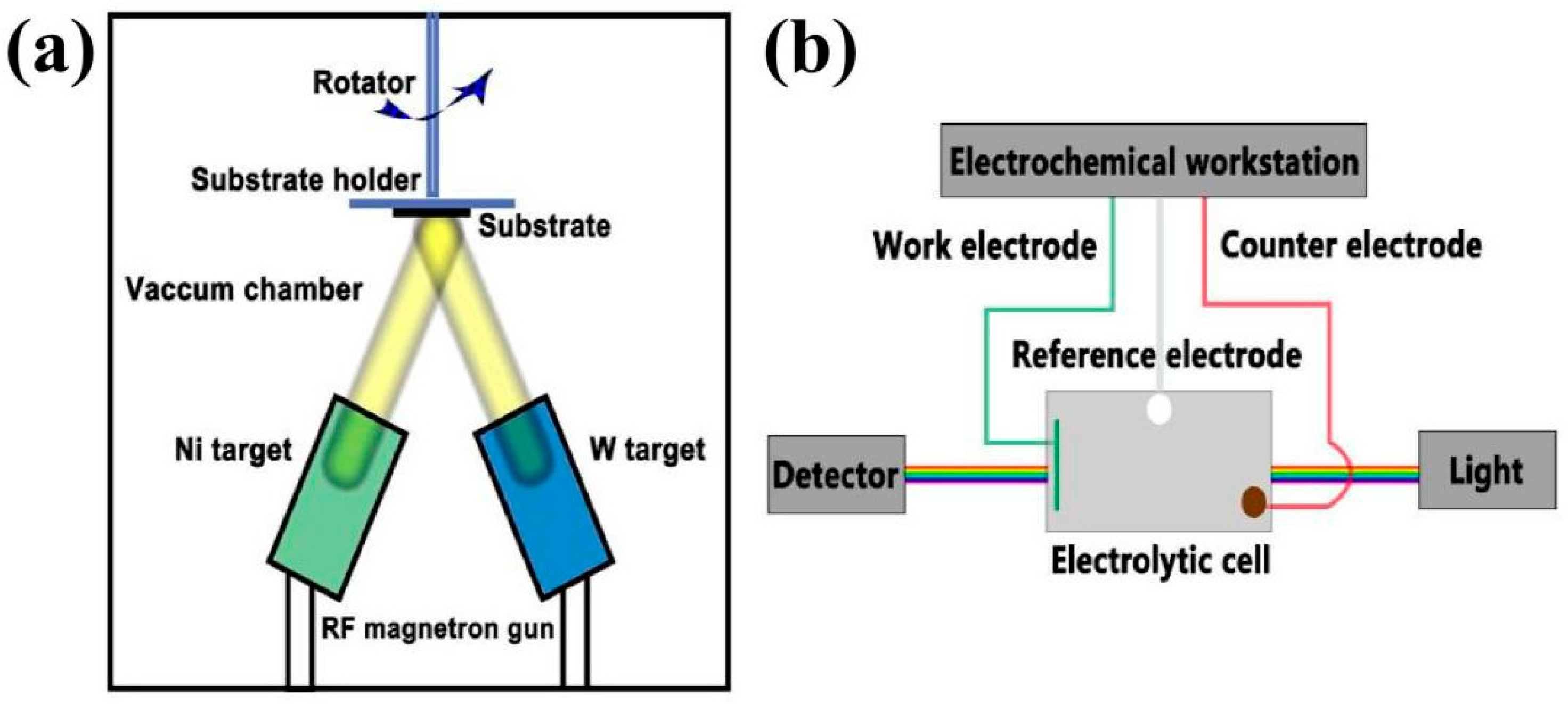
2.1. Preparation of the NiO and W-Doped NiO Films

The NiO and W-doped NiO (labeled as W-NiO) thin films were deposited onto ITO-coated glass (1 cm × 4 cm, sheet resistance Rs = 6 Ω/square) by radio frequency (RF) magnetron co-sputtering using W and a Ni metal target (99.99%) 50 mm in diameter, which is schematically shown in Figure 1a. W and Ni targets were faced together, the power ratio was set to 0:80 and 10:70, and the total power was set to 80 W. O2 content was set to 10% to ensure the transparency of the film, and the sputtering pressure was 1 Pa. Before the deposition, the ITO glass substrate was ultrasonically cleaned with acetone, ethanol, and deionized water for 30 min, respectively. The sputtering chamber was evacuated to 2 × 10⁻³ Pa, and the distance between the target and substrate was 6.5 cm. The substrate with no additional heating was kept rotating to ensure the uniformity of the as-deposited films. The target was pre-sputtered for 10 min to remove the surface contamination to guarantee the film quality.

2.2. Fabrication of the All-Solid-State ECDs

The all-solid-state ECDs with the structure of glass/ITO/W-NiO/LiTaO3/WO3/ITO were deposited by RF sputtering technology. The active area was 2 × 2 cm2. All layers were deposited in the same chamber without breaking the vacuum. The as-deposited ECD was treated at 300 °C in air for 3 h to improve the conductivity of the top ITO electrode. The deposition parameters for each layer are listed in Table 1.

2.3. Analytical Techniques

The investigation on the surface and the cross-sectional morphologies of the as-deposited NiO, W-NiO films, and all-solid-state ECD was performed by scanning electron microscopy (SEM) using a Zeiss Supra55 microscope (Carl Zeiss AG, Jena, Germany). The crystalline structure of the NiO and W-NiO films was studied by X-ray diffraction (XRD, PANalytical B. V. Model X′pert Pro, Almelo, Netherland) with a Cu Ka radiation (l = 1.54 Å) and a grazing angle of 0.5°. The composition of the NiO and W-NiO films was investigated by X-ray photoelectron spectroscopy (XPS) using a PHI 5700 ESCA System, (Physical Electronics Inc., Chanhassen, MN, USA). IR measurements were performed using Fourier transform IR spectrophotometer (Bruker Vetex 70, Karlsruhe, Germany) with a gold-coated integrating sphere in reflectance mode.
An in situ spectra-electrochemical test was carried out using an electrochemical station (CHI 660E, Shanghai Chenhua Instruments, Shanghai, China) and Vis-NIR fiber optic spectrometer (MAYA 2000-Pro, Ocean Optics, Dunedin, FL, USA) to investigate the EC performance of the NiO, W-NiO films, and ECD. The test equipment is schematically shown in Figure 1b. The NiO and W-NiO films were measured in a three-electrode system where the films, Pt wire, and Ag wire were used as the working electrode, counter electrode, and reference electrode, respectively. The electrolyte was 0.5 M LiClO4-PC (propylene carbonate). Chronoamperometry (CA) measurements were performed at ±1.5 V with a duration of 30 s. The potential range of cyclic voltammetry (CV) measurements was from −1.5 to 1.5 V. The scan rate of CV measurements was 50 mV/s. A two-electrode system was used for the test of ECD, where the top ITO layer near the WO3 layer was the working electrode and the bottom ITO layer was the reference and counter electrode. CA measurements were performed at ±3 V with durations of 60 and 300 s.

3. Results and Discussion

3.1. NiO and W-Doped NiO Films

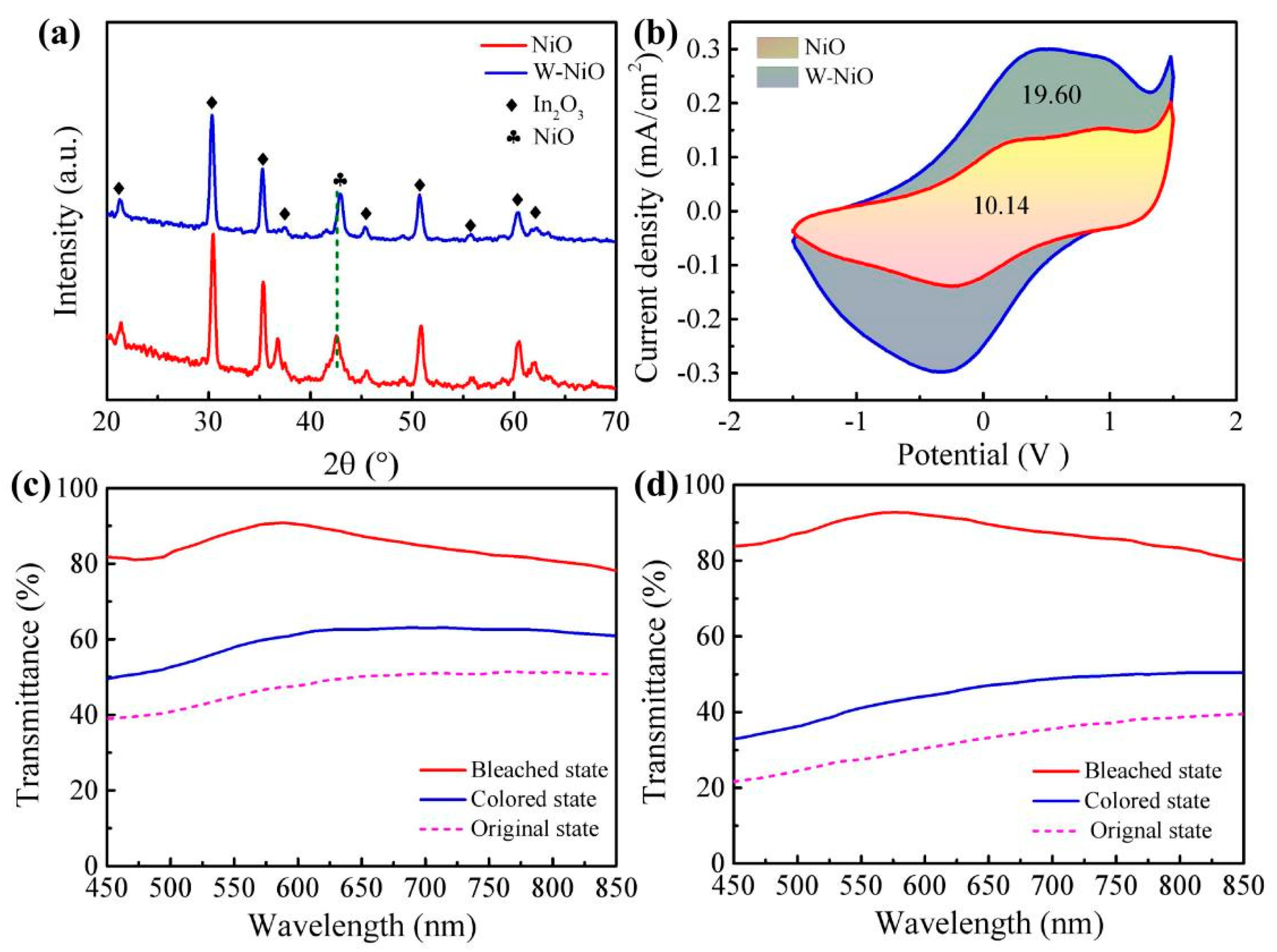
3.1.1. Structure and Composition of NiO and W-Doped NiO Films

Figure 2a shows the surface and cross-sectional SEM images of the NiO and W-NiO films. The surface morphology has a significant influence on the EC performance of the films because the EC reaction first occurs on the surface. The surface of the NiO and W-NiO films is similar and relatively smooth; it is composed of small particles, which is beneficial to the stability. From the cross-sectional images (Figure 2b,d), it can be seen that the thicknesses of the NiO and W-NiO films are about 135 nm.
The crystal structure of the NiO and W-NiO films on the ITO-coated glass is investigated by XRD, as exhibited in Figure 3a. Both the prepared films show the diffraction peaks of the ITO substrate (JCPDS 65-3170) [27]. A characteristic peak at around 43° can be observed in the patterns of NiO and W-NiO films, which is corresponding to the (200) plane (JCPDS 73-1519) of cubic NiO [28]. In addition, compared with pure NiO film, the diffraction peak of the W-NiO (200) plane shows a shift to high angle, indicating that the interplanar spacing becomes smaller after being doped by W, because the ionic radius of W (0.62 Å) is smaller than that of Ni (0.69 Å) [29]. Moreover, no other characteristic peaks corresponding to W or the W compound are detected in the W-NiO film, which implies that W is completely incorporated into the lattice of NiO or the W compound exists in amorphous form in the W-NiO film.
XPS measurement is carried out to analyze the composition and chemical state of the element of the NiO and W-NiO films, as shown in Figures S1 and S2. The spectra of the two samples show that the NiO film contains Ni, O, and C, while W-NiO additionally contains W with a peak at around 35.8 eV corresponding to W 4f. Ni 2p3/2 and W 4f XPS high-resolution spectra of the W-NiO film are presented in Figure S2. The binding energy at 855.5 eV is assigned to the Ni 2p3/2 peak with a satellite peak at 862.2 eV. The Ni 2p3/2 peak can be fitted to two peaks corresponding to two valence states of Ni, which are Ni2+ in Ni-O bonds and Ni3+ mainly in Ni2O3, respectively, as shown in Figure S2a. It can be seen that Ni in the as-prepared W-NiO is mainly Ni2+ [30]. The W 4f XPS high-resolution spectra can be fitted to W4f7/2 and W4f5/2 components, with the binding energies of 34.3 and 36.4 eV, respectively [31]. The results show that the W in the W-NiO film is mainly W6+ with a proportion of 75.3%.

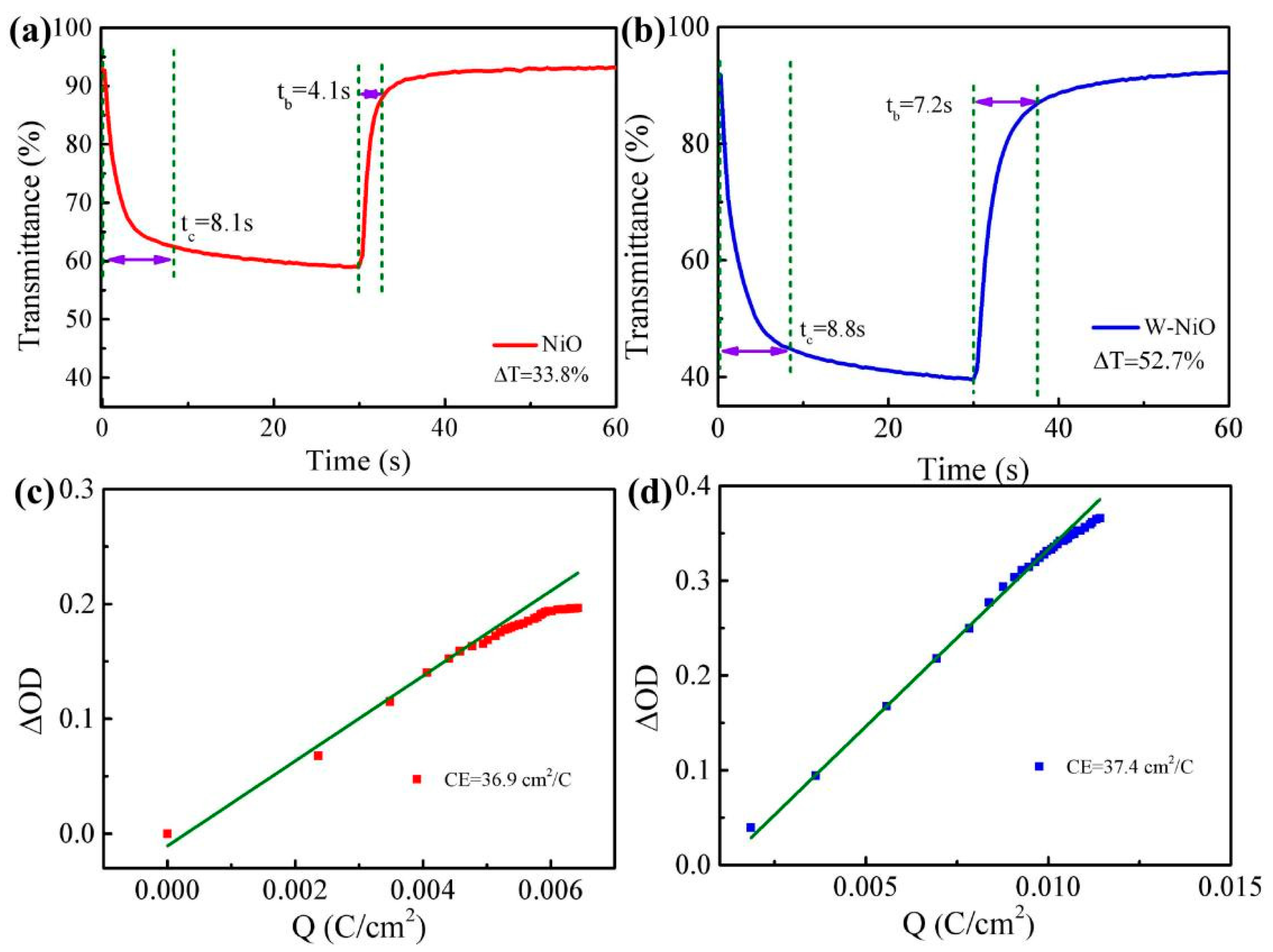
3.1.2. EC Performances of NiO and W-Doped NiO Films

Figure 3b presents the CV curves of the NiO and W-NiO films performed at a scan rate of 50 mV/s. Both the films show obvious redox peaks corresponding to the conversion of Ni2+ and Ni3+ in the films, which is accompanied by the changes of colored and bleached states of the films. Compared with the NiO film, the W-NiO film exhibits larger current density, and the charge density obtained by integrating the current density is 19.6 mC/cm2, which is almost twice as much as that of NiO, indicating that W doping is conducive to improve the activity of the EC reaction of NiO. Due to the large difference between the stable valence states of Ni (2+) and W (6+ and 5+), the W ions of high oxidation state (6+ and 5+) will cause a large disturbance in the lattice around the W cation inserted into the Ni site. Thus, the crystal structure of NiO becomes less dense compared with pure NiO, which will lead to a large number of lattice boundaries, producing more lattice defects and active sites for the electrochromic reaction.
The EC performances of the films are measured, and the transmittance spectra of the NiO and W-NiO films are displayed in Figure 3c,d. The as-prepared W-NiO film shows a low transmittance in original state, which is about 20% lower than that of NiO. When the negative voltage to the film is applied, the Li ions are injected into the film, and the film switches to the bleached state. The films switch to the colored state after the extraction of Li ions, and the transmittance of the colored state of the two films is higher than that of the original state, which may be related to the mechanism of NiO in Li salts electrolytes. The optical modulation of the W-NiO film is obviously larger compared with NiO due to more ions participating in the reaction, which can be seen from the CV results.
The response time, defined as the time required to reach 90% of total transmittance modulation in the EC process [32], is one of the most important evaluation criterion of the EC materials. Figure 4a and b show the time-dependent transmittance spectra of the NiO and W-NiO films. The optical modulation of the NiO film at 550 nm is 33.8% with the coloring time (tc) of 8.1 s and bleaching time (tb) of 4.1 s. The W-NiO film exhibits an obvious increase in optical modulation, which reaches 52.7%, while the tc hardly changes. The tb increases due to the increase in the optical modulation [33].
Coloration efficiency (CE), which means the change of optical density (ΔOD) per unit charge (Q), is an index to evaluate the energy-saving effect of the EC materials. It can be calculated according to the following equations [34]:
Δ OD = log ( t b / t c )
CE = Δ OD / Δ Q .
The NiO and W-NiO films show similar CE values, which are 36.9 and 37.4 cm2/C, respectively, as exhibited in Figure 4c,d. The above results indicate that the W doping can significantly improve the optical modulation of the NiO film without affecting other performances such as the response speed and CE.

3.2. All-Solid-State ECD Based on W-NiO Film

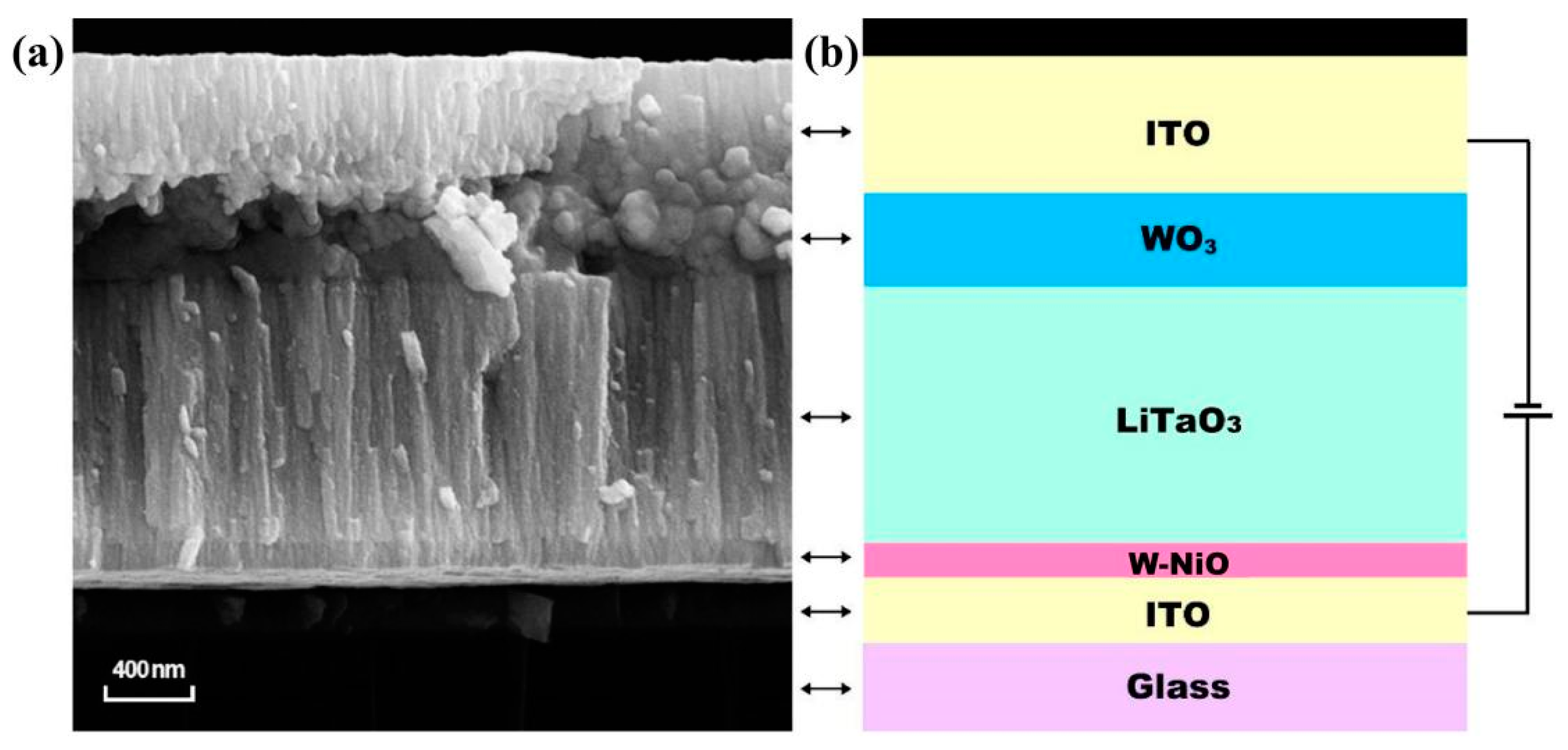
3.2.1. Morphology of the ECD

The EC performances of W-NiO film confirm that it has the potential to replace NiO as a complementary layer of WO3 in all-solid-state ECDs. Therefore, an ECD with structure of glass/ITO/W-NiO/LiTaO3/WO3/ITO is prepared, and the cross-section morphology of the ECD is characterized. Figure 5 shows the cross-section SEM image and the scheme of the ECD. The ECD exhibits a clearly identified five-layer structure, which are ITO, W-NiO, LiTaO3, WO3, and ITO from bottom to top with the thicknesses of 200, 135, 1190, 440, and 620 nm, respectively. The closely connected interfaces indicate the physical and chemical stability of the ECD, which is important to the lifetime of the ECD.

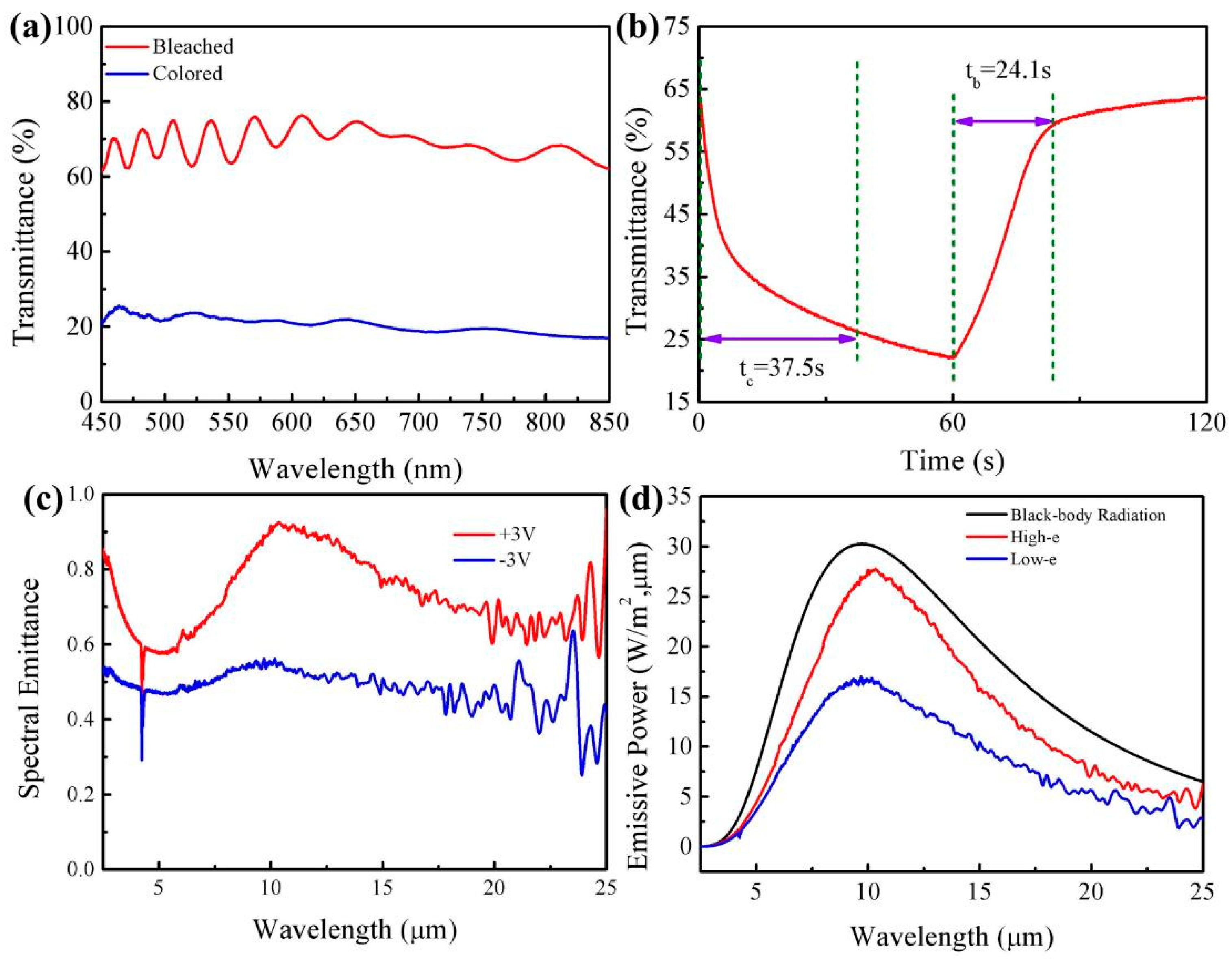
3.2.2. EC Performances of the ECD

The EC performances of the ECD are investigated. Figure 6a displays the transmittance spectra of the bleached and colored ECD after 150 cycles. The average transmittance spectra of the bleached state and colored state are 68.9% and 20.4%, respectively, with an average optical modulation of 48.5%. The time-dependent transmittance spectra in Figure 6b indicates that the optical modulation of the ECD in 550 nm is 41.7% and the response speed is 37.5 s for coloring and 24.1 s for bleaching. The cyclic stability of the ECD is also studied and shown in Figure S3. The transmittance of the bleached state maintains stability in the first 70 cycles; then, it decreases slightly, and the transmittance of the colored state slowly goes down and finally tends to be stable. Figure S4 exhibits the transmittance spectra and digital photos of the ECD with a switching time of 300 s. The transmittance of the ECD is lower than 10% after 300 s of coloring, and the average optical modulation is 60.8%. The ECD with pure NiO is also prepared, and the performances are presented in Figures S5 and S6. The initial transmittance modulation at 550 nm is 43.8%, which is much larger than that of ECD with W-NiO. However, it degrades rapidly due to the obvious decrease in the transmittance of the bleached state during cycling, indicating that W doping is beneficial to improve the stability of the ECD. The optical modulation of the ECD with pure NiO decreases to 30.8% after cycling with response times of 44.4 s for coloring and 26.3 s for bleaching, respectively, which is a little longer than that of the ECD with W-NiO. The EC performances of the modified NiO films and devices reported previously are listed in Table S1 for comparison.
Infrared emittance (ε), including spectral emittance and emissive power, is one of the most important parameters for applications in the space thermal control field. However, there are few reports on the infrared emittance control of inorganic all-solid-state ECDs. According to Kirchhoff’s law, the absorptivity is equal to the emittance for an object in thermal equilibrium [35]. The transmittance of the ITO glass substrate is almost zero in the wavelength range of 2.5–25 μm [35]. Thus, the spectral emittance can be obtained by the reflectance of the ECD. The spectral emittance of the prepared ECD is illustrated in Figure 6c. The absorptivity increases and the reflectance decreases when the ECD is colored at −3 V; thus, the ECD exhibits a high emittance of 0.77. The absorptivity of the ECD decreases, and the ECD switches to the low emittance state (0.49) when the ECD is bleached at +3 V. The ECD exhibits an excellent emittance regulation ability with an emittance modulation value of 0.28.
Emissive power is defined as the ratio of the radiant energy of an object at a certain temperature to the radiant energy of a standard blackbody and can be calculated according to the equations as follows [35]:
B λ = c 1 λ 5 exp [ c 2 ( λ T ) ] 1
ε = λ m i n λ m a x ( 1   ρ λ ) B λ d λ λ m i n λ m a x B λ d λ
Bλ is radiation power at a certain wavelength, and c1 and c2 are the first and second radiation constant (c1 = 3.7418 × 10⁸ W·μm4/m2, c2 = 1.4388 × 104 μm·K).
Figure 6d shows the emissive power spectra of the ECD in different emittance states and the ideal black-body spectrum at 298 K. The emissive power of the ECD at −3 and +3 V is 287 and 182 W/m2 respectively, which indicates that the regulated emissive power of the ECD is 105 W/m2 when applied in intelligent thermal control.

4. Conclusions

In this work, NiO and W-doped NiO films are prepared by magnetron sputtering and the surface morphology, crystalline structure, chemical composition, electrochemical properties, and EC performances of the films are investigated. The results show that the charge density of NiO film increased remarkably after doping by W element; thus, the W-NiO exhibits high optical modulation of 52.7%, which is much larger than the value of NiO (33.8%). Meanwhile, the other EC indexes such as response time and CE are almost unaffected, indicating that W-NiO film is promising to replace NiO as a component of all solid-state ECDs. The W-NiO film is applied to an all-solid-state ECD with the structure of glass/ITO/W-NiO/LiTaO3/WO3/ITO. The ECD shows a relatively high optical modulation of 41.7% at 550 nm with a response time of 37.5 s for coloring and 24.1 s for bleaching and excellent emittance regulation ability of 0.28 in wavelength of 2.5–25 μm. The above results demonstrate that the ECD using W-NiO as a complementary layer can not only be applied in the smart window field but also show great potential in thermal control devices.

Supplementary Materials

The following are available online at https://www.mdpi.com/article/10.3390/coatings12020118/s1, Figure S1: XPS spectra of the NiO and W-NiO films, Figure S2: (a) High-resolution spectra of Ni 2p. (b) High-resolution spectra of W4f, Figure S3: Cyclic stability of the ECD with W-NiO measured at ±3 V with a duration of 60 s, Figure S4: Transmittance spectra and digital photos of the ECD with W-NiO measured at ±3 V with a duration of 300 s, Figure S5: (a) Time dependent transmittance spectra, (b) Transmittance spectra of the ECD with NiO after 150 cycles, Figure S6: Cyclic stability of the ECD with NiO measured at ±3 V with a duration of 60 s, Table S1: Comparison of the W-NiO film and ECD with previously reported data.

Author Contributions

X.Z. (Xin Zhao) and Z.Y. carried out the tests and wrote the manuscript, X.Z. (Xin Zhao), X.Z. (Xiang Zhang), W.L., C.Y., W.S. and H.Z. performed the analysis of the results and assisted in the test, X.Z. (Xiang Zhang), Y.L. and Z.Y. contributed to the concept and modified the manuscript. All authors have read and agreed to the published version of the manuscript.

Funding

This research received no external funding.

Institutional Review Board Statement

Not applicable.

Informed Consent Statement

Not applicable.

Data Availability Statement

The data presented in this study are available on request from the corresponding author.

Conflicts of Interest

The authors declare no conflict of interest.

References

  1. Granqvist, C.G. Electrochromics for smart windows: Oxide-based thin films and devices. Thin Solid Films 2014, 564, 1–38. [Google Scholar] [CrossRef]
  2. Dong, D.; Djaoued, H.; Vienneau, G.; Robichaud, J.; Brown, D.; Brüning, R.; Djaoued, Y. Electrochromic and colorimetric properties of anodic NiO thin films: Uncovering electrochromic mechanism of NiO. Electrochim. Acta 2020, 335, 135648. [Google Scholar] [CrossRef]
  3. Pan, J.; Zheng, R.; Wang, Y.; Ye, X.; Wan, Z.; Jia, C.; Weng, X.; Xie, J.; Deng, L. A high-performance electrochromic device assembled with hexagonal WO3 and NiO/PB composite nanosheet electrodes towards energy storage smart window. Sol. Energy Mater. Sol. Cells 2020, 207, 110337. [Google Scholar] [CrossRef]
  4. Zhao, Q.; Wang, J.; Cui, Y.; Ai, X.; Chen, Z.; Cao, C.; Xu, F.; Gao, Y. The discovery of conductive ionic bonds in NiO/Ni transparent counter electrodes for electrochromic smart windows with an ultra-long cycling life. Mater. Adv. 2021, 2, 4667–4676. [Google Scholar] [CrossRef]
  5. Xu, Z.; Li, W.; Huang, J.; Guo, X.; Liu, Q.; Yu, R.; Miao, W.; Zhou, B.; Guo, W.; Liu, X. Flexible, controllable and angle-independent photoelectrochromic display enabled by smart sunlight management. Nano Energy 2019, 63, 103830. [Google Scholar] [CrossRef]
  6. Zhang, X.; Li, W.; Li, X.; Wang, L.; Sun, W.; Zhang, H.; Wang, J.; Zhao, J.; Li, Y. Bio-inspired electrochromic skin based on tungsten oxide. Sol. Energy Mater. Sol. Cells 2021, 230, 111195. [Google Scholar] [CrossRef]
  7. Shah, K.W.; Wang, S.X.; Soo, D.X.Y.; Xu, J. Viologen-based electrochromic materials: From small molecules, polymers and composites to their applications. Polymers 2019, 11, 1839. [Google Scholar] [CrossRef] [PubMed] [Green Version]
  8. Xu, Z.; Qiu, W.; Fan, X.; Shi, Y.; Gong, H.; Huang, J.; Patil, A.; Li, X.; Wang, S.; Lin, H.; et al. Stretchable, stable, and degradable silk fibroin enabled by mesoscopic doping for finger motion triggered color/transmittance adjustment. ACS Nano 2021, 15, 12429–12437. [Google Scholar] [CrossRef] [PubMed]
  9. Mandal, J.; Du, S.; Dontigny, M.; Zaghib, K.; Yu, N.; Yang, Y. Li4Ti5O12: A visible-to-infrared broadband electrochromic material for optical and thermal management. Adv. Funct. Mater. 2018, 28, 1–8. [Google Scholar] [CrossRef] [Green Version]
  10. Zhang, X.; Li, W.; Chen, X.; Zhao, Y.; Wang, L.; Chen, M.; Li, Z.; Li, Y. Inorganic all-solid-state electrochromic devices with reversible color change between yellow-green and emerald green. Chem. Commun. 2020, 56, 10062–10065. [Google Scholar] [CrossRef]
  11. Huang, H.; Tian, J.; Zhang, W.K.; Gan, Y.P.; Tao, X.Y.; Xia, X.H.; Tu, J.P. Electrochromic properties of porous NiO thin film as a counter electrode for NiO/WO3 complementary electrochromic window. Electrochim. Acta 2011, 56, 4281–4286. [Google Scholar] [CrossRef]
  12. Li, W.; Zhang, X.; Chen, X.; Zhao, Y.; Sun, W.; Xiao, Y.; Li, S.; Zhao, J.; Li, Y. Long life all-solid-state electrochromic devices by annealing. Sol. Energy Mater. Sol. Cells 2021, 224, 110992. [Google Scholar] [CrossRef]
  13. Green, S.; Backholm, J.; Georén, P.; Granqvist, C.G.; Niklasson, G.A. Electrochromism in nickel oxide and tungsten oxide thin films: Ion intercalation from different electrolytes. Sol. Energy Mater. Sol. Cells 2009, 93, 2050–2055. [Google Scholar] [CrossRef] [Green Version]
  14. Sonavane, A.C.; Inamdar, A.I.; Dalavi, D.S.; Deshmukh, H.P.; Patil, P.S. Simple and rapid synthesis of NiO/PPy thin films with improved electrochromic performance. Electrochim. Acta 2010, 55, 2344–2351. [Google Scholar] [CrossRef]
  15. Zhao, Y.; Zhang, X.; Chen, X.; Li, W.; Wang, L.; Li, Z.; Zhao, J.; Endres, F.; Li, Y. Preparation of Sn-NiO films and all-solid-state devices with enhanced electrochromic properties by magnetron sputtering method. Electrochim. Acta 2021, 367, 137457. [Google Scholar] [CrossRef]
  16. Firat, Y.E.; Peksoz, A. Efficiency enhancement of electrochromic performance in NiO thin film via Cu doping for energy-saving potential. Electrochim. Acta 2019, 295, 645–654. [Google Scholar] [CrossRef]
  17. Choi, D.; Son, M.; Im, T.; Ahn, S.H.; Lee, C.S. Microstructure control of NiO-based ion storage layer with various sized NiO particles to evaluate the electrochromic performance. Mater. Chem. Phys. 2020, 249, 123121. [Google Scholar] [CrossRef]
  18. Yu, J.H.; Nam, S.H.; Gil, Y.E.; Boo, J.H. The effect of ammonia concentration on the microstructure and electrochemical properties of NiO nanoflakes array prepared by chemical bath deposition. Appl. Surf. Sci. 2020, 532, 147441. [Google Scholar] [CrossRef]
  19. Yuan, Y.F.; Xia, X.H.; Wu, J.B.; Chen, Y.B.; Yang, J.L.; Guo, S.Y. Enhanced electrochromic properties of ordered porous nickel oxide thin film prepared by self-assembled colloidal crystal template-assisted electrodeposition. Electrochim. Acta 2011, 56, 1208–1212. [Google Scholar] [CrossRef]
  20. Penin, N.; Rougier, A.; Laffont, L.; Poizot, P.; Tarascon, J.M. Improved cyclability by tungsten addition in electrochromic NiO thin films. Sol. Energy Mater. Sol. Cells 2006, 90, 422–433. [Google Scholar] [CrossRef]
  21. Pereira, S.; Gonçalves, A.; Correia, N.; Pinto, J.; Pereira, L.; Martins, R.; Fortunato, E. Electrochromic behavior of NiO thin films deposited by e-beam evaporation at room temperature. Sol. Energy Mater. Sol. Cells 2014, 120, 109–115. [Google Scholar] [CrossRef]
  22. Ren, Y.; Zhou, X.; Zhang, H.; Lei, L.; Zhao, G. Preparation of a porous NiO array-patterned film and its enhanced electrochromic performance. J. Mater. Chem. C 2018, 6, 4952–4958. [Google Scholar] [CrossRef]
  23. Yang, H.; Yu, J.H.; Seo, H.J.; Jeong, R.H.; Boo, J.H. Improved electrochromic properties of nanoporous NiO film by NiO flake with thickness controlled by aluminum. Appl. Surf. Sci. 2018, 461, 88–92. [Google Scholar] [CrossRef]
  24. Chang, J.Y.; Chen, Y.C.; Wang, C.M.; Chen, Y.W. Electrochromic properties of Li-Doped NiO films prepared by RF magnetron sputtering. Coatings 2020, 10, 87. [Google Scholar] [CrossRef] [Green Version]
  25. Azevedo, C.F.; Balboni, R.D.C.; Cholant, C.M.; Moura, E.A.; Lemos, R.M.J.; Pawlicka, A.; Gündel, A.; Flores, W.H.; Pereira, M.; Avellaneda, C.O. New thin films of NiO doped with V2O5 for electrochromic applications. J. Phys. Chem. Solids 2017, 110, 30–35. [Google Scholar] [CrossRef]
  26. Avendaño, E.; Azens, A.; Niklasson, G.A.; Granqvist, C.G. Electrochromism in nickel oxide films containing Mg, Al, Si, V., Zr, Nb, Ag, or Ta. Sol. Energy Mater. Sol. Cells 2004, 84, 337–350. [Google Scholar] [CrossRef]
  27. Yu, L.; Huang, Y.; Xiao, G.; Li, D. Application of long wavelength visible light (λ > 650 nm) in photocatalysis with a p-CuO–n-In2O3 quantum dot heterojunction photocatalyst. J. Mater. Chem. A 2013, 1, 9637–9640. [Google Scholar] [CrossRef]
  28. Zhou, K.; Qi, Z.; Zhao, B.; Lu, S.; Wang, H.; Liu, J.; Yan, H. The influence of crystallinity on the electrochromic properties and durability of NiO thin films. Surf. Interfaces 2017, 6, 91–97. [Google Scholar] [CrossRef]
  29. Hartman, P.; Chan, H.K. Application of the periodic bond chain (PBC) theory and attachment energy consideration to derive the crystal morphology of hexamethylmelamine. Pharm. Res. 1993, 10, 1052–1058. [Google Scholar] [CrossRef] [PubMed]
  30. Biesinger, M.C.; Payne, B.P.; Lau, L.W.M.; Gerson, A.; Smart, R.S.C. X-ray photoelectron spectroscopic chemical state Quantification of mixed nickel metal, oxide and hydroxide systems. Surf. Interface Anal. 2009, 41, 324–332. [Google Scholar] [CrossRef]
  31. Zhang, J.; Tu, J.P.; Xia, X.H.; Qiao, Y.; Lu, Y. An all-solid-state electrochromic device based on NiO/WO3 complementary structure and solid hybrid polyelectrolyte. Sol. Energy Mater. Sol. Cells 2009, 93, 1840–1845. [Google Scholar] [CrossRef]
  32. Chen, P.W.; Chang, C.T.; Ko, T.F.; Hsu, S.C.; Li, K.D.; Wu, J.Y. Fast response of complementary electrochromic device based on WO3/NiO electrodes. Sci. Rep. 2020, 10, 1–12. [Google Scholar] [CrossRef] [PubMed]
  33. Li, W.; Zhang, X.; Chen, X.; Zhao, Y.; Wang, L.; Chen, M.; Li, Z.; Zhao, J.; Li, Y. Lithiation of WO3 films by evaporation method for all-solid-state electrochromic devices. Electrochim. Acta 2020, 355, 136817. [Google Scholar] [CrossRef]
  34. Li, W.; Zhang, X.; Chen, X.; Zhao, Y.; Wang, L.; Chen, M.; Zhao, J.; Li, Y.; Zhang, Y. Effect of independently controllable electrolyte ion content on the performance of all-solid-state electrochromic devices. Chem. Eng. J. 2020, 398, 125628. [Google Scholar] [CrossRef]
  35. Zhang, X.; Tian, Y.; Li, W.; Dou, S.; Wang, L.; Qu, H.; Zhao, J.; Li, Y. Preparation and performances of all-solid-state variable infrared emittance devices based on amorphous and crystalline WO3 electrochromic thin films. Sol. Energy Mater. Sol. Cells 2019, 200, 109916. [Google Scholar] [CrossRef]
Figure 1. Schematic diagram of the equipment used for preparation and measurement. (a) RF magnetron co-sputtering equipment. (b) In situ spectral–electrochemical testing equipment.
Coatings 12 00118 g001
Figure 2. SEM images of the NiO and W-NiO films. (a) Surface and (b) cross-sectional SEM images of the NiO film. (c) Surface and (d) cross-sectional SEM images of the W-NiO film.
Coatings 12 00118 g002
Figure 3. (a) XRD patterns. (b) CV curves of the NiO and W-NiO films. (c) Transmittance spectra of NiO film. (d) Transmittance spectra of W-NiO film.
Coatings 12 00118 g003
Figure 4. Time-dependent transmittance spectra (a) and CE (c) of the NiO film at 550 nm. Time-dependent transmittance spectra (b) and CE (d) of the W-NiO film at 550 nm.
Coatings 12 00118 g004
Figure 5. Cross-sectional SEM image (a) and schematic diagram (b) of the ECD.
Coatings 12 00118 g005
Figure 6. (a) Transmittance spectra, (b) Time-dependent transmittance spectra, (c) Spectral emittance curves, and (d) Emissive power curves of the ECD with W-NiO after 150 cycles.
Coatings 12 00118 g006
Table 1. Deposition parameters for the layers in the all-solid-state ECDs.
LayerO2 (%)Pressure (Pa)Power (W)Time (min)
W-NiO101.010:70120
LiTaO351.0100480
NiO501.0100150
ITO10.45060
Publisher’s Note: MDPI stays neutral with regard to jurisdictional claims in published maps and institutional affiliations.

