Article

Thin Layers of SrTiO3-TiO2 with Eutectic Composition for Photoelectrochemical Water Splitting

by
Jaroslaw Sar
1,2,*,
Katarzyna Kołodziejak
1,2,
Krzysztof Orliński
1,
Michal Gajewski
1,
Marian Teodorczyk
1 and
Dorota Anna Pawlak
1,2
1
Łukasiewicz Research Network—Institute of Microelectronics and Photonics, Al. Lotników 32/46, 02-668 Warsaw, Poland
2
Centre of Excellence ENSEMBLE3 Sp. z o. o., Wolczynska Str. 133, 01-919 Warsaw, Poland
*
Author to whom correspondence should be addressed.
Coatings 2022, 12(12), 1876; https://doi.org/10.3390/coatings12121876
Submission received: 2 November 2022 / Revised: 24 November 2022 / Accepted: 29 November 2022 / Published: 2 December 2022
(This article belongs to the Special Issue Advanced Photo- and Electrocatalytic Surface Applications)

Abstract

:
Hydrogen as a potential fuel of the future can be produced in a photoelectrochemial water splitting process. Herein, we demonstrate the fabrication of photoelectrochemical electrodes based on SrTiO3-TiO2 with a eutectic composition on titanium and conductive glass FTO (fluorine doped tin oxide) substrates by magnetron sputtering. The XRD and SEM/EDS reveal the amorphous nature and homogeneity of the sputtered material. The influence of the layer thickness on the photoactivity was investigated. There were three-layer thicknesses (50, 350, and 750 nm) selected by sputtering for 12, 80 and 220 min for the preparation of photoelectrodes. The photoelectrochemical analysis confirms the photoactivity of the obtained layers under illumination with a xenon lamp (600 mW/cm2). The highest photocurrent density of 11.8 × 10⁻³ mAcm−2 at 1.2 V vs. SCE was recorded for a layer thickness of 50 nm on titanium as better matching between the Ti work function and the conduction band.

1. Introduction

The alternative to hydrogen production through conventional water electrolysis is through photoelectrochemical (PEC) cells. PEC water splitting implies the junction of semiconductors and liquid, where the sunlight is captured, and water molecules are directly electrolyzed producing gaseous hydrogen and oxygen. PEC cells are built from photoactive semiconductor material, n-type for the photoanode and p-type for the photocathode. Photons with energy equal to or higher than the band gap generate electron–hole pairs in the semiconductor. Electrons travel from the photoanode to the photocathode where they reduce H+ into H2. At the same time, the holes react with water molecules producing O2. From the large number of semiconductors, only a few fulfill the necessary criteria for efficient separation of a photogenerated electron–hole, photoresponse matched to the solar spectrum and stability under harsh operating conditions [1]. The potential required for thermodynamic water splitting is 1.23 V, but taking into account the energy losses, the optimum band gap of the semiconductor should be around 2 eV [2]. Moreover, the position of the conduction band should be more negative than the hydrogen evolution potential, while the valence band edges should be more positive than the oxygen evolution potential [3]. None of the semiconductors can satisfy the criteria of stability, band gap and position of band gap edges. Materials that meet the above criteria are eutectic composites. Eutectic composites are characterized by the formation of two or more non-mixable crystals from a completely mixable melt, which leads to the formation of self-organized micro/nanostructures [4]. Directionally solidified eutectics (DSE) may be defined as composite materials with a complex and homogeneous micro- or nanostructure, which controls their properties [5]. Eutectic composites are broadly investigated in terms of special geometrical motifs (lamellar, fibrous, globular and spiral) [6,7], the plasmonic effect [8,9], electromagnetic properties [10] and, recently, photoelectrochemistry [11,12,13]. Eutectic composites are able to compete with other materials because of their (i) high crystallinity (as single crystals) [14], (ii) sharp interfaces between the component phases [15], (iii) potential use in designing materials with various component materials, enabling broadband absorption (UV-Vis) and (iv) utilization phases, which are hard to achieve or are unavailable in another way. The aim of this work was to fabricate the photoelectrochemically active layers of a SrTiO3-TiO2 composite with a eutectic composition by magnetron sputtering. Both components of the SrTiO3-TiO2 eutectic system have a wide bag gap corresponding to the absorption of UV light [16,17], and their valence and conduction bands overlap the water redox potentials [18]. The layers were deposited on titanium and glass with fluorine doped tin oxide (FTO) with a controllable sputtering time in order to investigate the effect of layer thickness on the photoelectrochemical performance. The deposition of SrTiO3 and TiO2 is a common subject in areas such as computer memories, sensors, IR detectors, catalysts and others. Researchers use the advantages of magnetron sputtering to modify and improve the properties of materials. It can be found in the literature that magnetron sputtering was used for uniform doping to get Al-SrTiO3 [19] and Nb-TiO2 [20]; for the sandwich structure of SrTiO3/TiO2/SrTiO3 [21]; for SrTiO3-TiO2 heterostructures [22,23,24]; and for the deposition of TiO2 on glass, Pt, Si [25] and SrTiO3 thin films, for the application in solar energy harvesting [26]. In this work, we present the simultaneous sputtering of SrTiO3 and TiO2 in order to form a homogeneous distribution of both components on Ti and FTO substrates. It is possible because of the preparation of the SrTiO3-TiO2 sputtering target with the eutectic composition and use for photoelectrochemical water splitting.

2. Materials and Methods

2.1. Magnetron Sputtering

Thin layers of SrTiO3-TiO2 eutectic composites were deposited by magnetron sputtering. The ceramic target for sputtering was obtained by mixing SrO and TiO2 powders in a ratio corresponding to a eutectic composition of 23 mol. % of SrO and 77 mol. % of TiO2 [27]. The mixture of powders was preheated at 70 °C and then synthesized at 1100 °C. The prepared material was grated with a 10% water solution of PVA to form granules. The ceramic target in a disk shape with a diameter of 100 mm and thickness of 5 mm was pressed and sintered at 1300 °C for 12 h in air. Magnetron sputtering was performed in a ULVAC vacuum sputtering machine. Before the sputtering, the substrate was cleaned by successive sonication in water and ethanol for 10 min each. The distance between the target and the substrate was set at 43 mm. The substrate temperature was ambient before the sputtering, and it was not heated or cooled down during the process. Its temperature changed to around 60 °C while heating from the generated plasma. The relationship between the sputtering time and the layer thickness was investigated.

2.2. Material Characterization

The thickness of the deposited layer was analyzed by a Veeco Dektak 150 surface profilometer. During the initial deposition, the substrate surface was partially covered in order to create the gap between the bare substrate and the deposited material. The X-ray powder diffraction analysis was performed on the as-grown samples using a Siemens D500 powder diffractometer equipped with a semiconductor Si:Li detector from 20–120° with the θ/2θ scanning mode with a step size of 0.02º and a counting time of 10 s/step, using Cu Kα radiation (1.5406 Å). Phases were identified using the International Centre for Diffraction Data PDF4+ database [28]. Additionally, the deposited layers were analyzed by grazing incidence X-ray diffraction (GIXD). SEM images were performed on the as-deposited samples using a Cross Beam Workstation (Carl Zeiss SMT, Oberkochen, Germany) combined with an energy dispersive X-ray spectrometer.

2.3. Photoelectrochemical (PEC) Analysis

The photoelectrochemical analysis was performed in a Teflon/PTFE cell with a quartz window. Measurements used a three-electrode configuration: SrTiO3-TiO2 electrodes served as a working electrode (WE), a saturated calomel electrode (SCE) served as the reference electrode (RE) and a platinum electrode as the counter electrode (CE). A mixture of H2SO4 and Na2SO4 with a pH of 2 was used as an electrolyte. All PEC was performed in CHI-660D potentiostat using open-circuit potential (OCP) mode versus time and cyclic voltammetry in the potential range of −0.3–1.7 V and a 10 mV/s scan rate. Electrochemical impedance spectroscopy (EIS) was carried out at 1 V vs. SCE potential in the frequency range from 1 MHz to 0.01 Hz. All techniques were used with illumination and in dark conditions. A 150 W xenon lamp from solar light with 600 mA/cm2 irradiation calibrated by a Solar Light PMA 2144 Class II pyranometer was used as a light source.

3. Results and Discussion

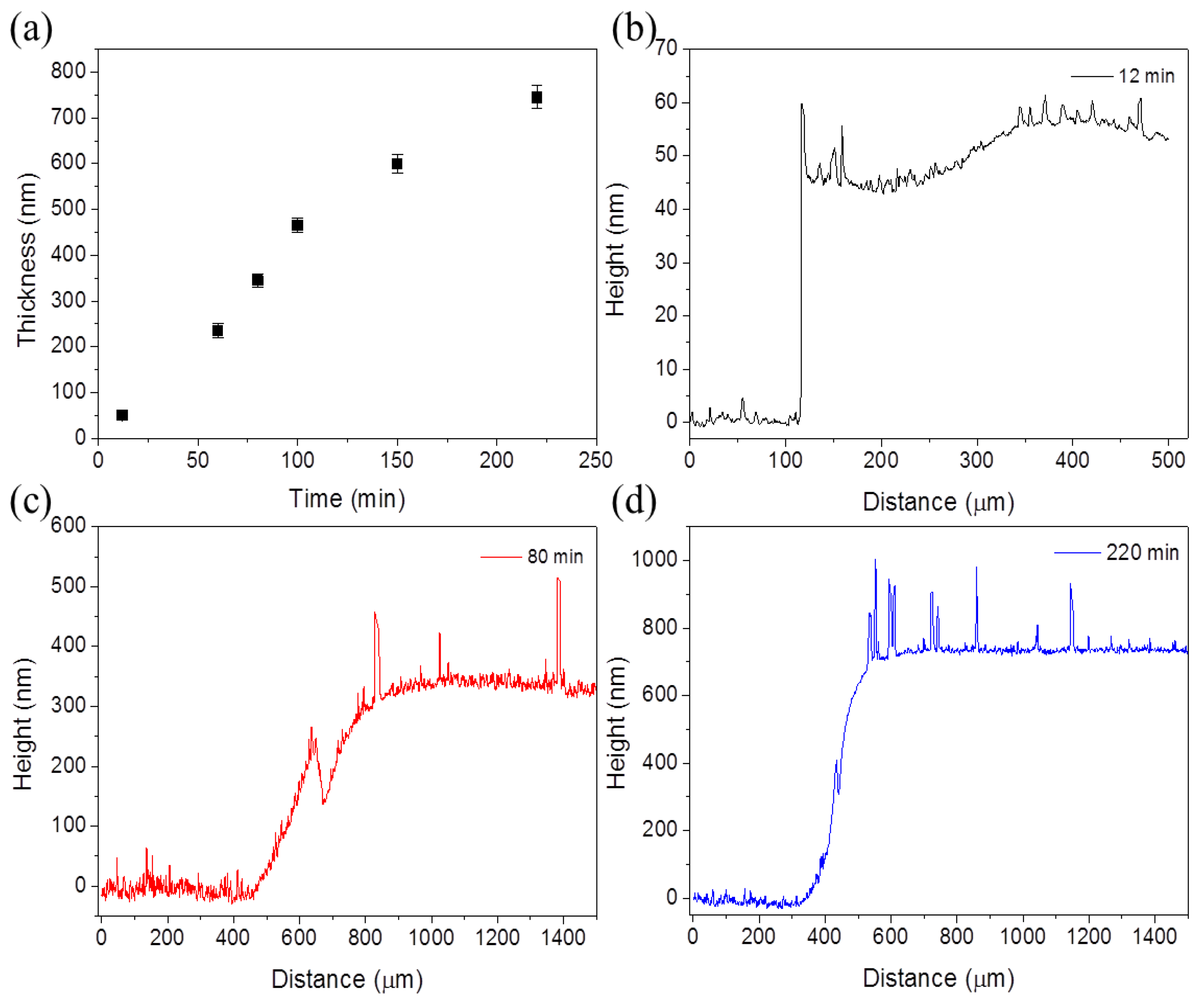
3.1. Layers of SrTiO3-TiO2-Eutectic Composition

The SrTiO3-TiO2 layers were deposited by sputtering on two types of substrates: titanium and glass with fluorine doped tin oxide (FTO). These depositions were initially performed to define the relationship between sputtering time and layer thickness. The deposition parameters, such as PAr vacuum level expressed in argon pressure, power of the device causing the voltage to be applied between the substrate and the target, target to substrate distance, sputtering time and the measured thickness of the layer are presented in Table 1. The layer thickness increases logarithmically with increasing sputtering time (Figure 1a). Based on the initial depositions, there were three deposition settings selected to obtain layer thicknesses around 50, 350 and 750 nm (Figure 1b–d). The high resolution of the profilometer also allowed for the determination of measuring point inaccuracies related to roughness and/or unwanted contamination of the substrate, as well as the layer.

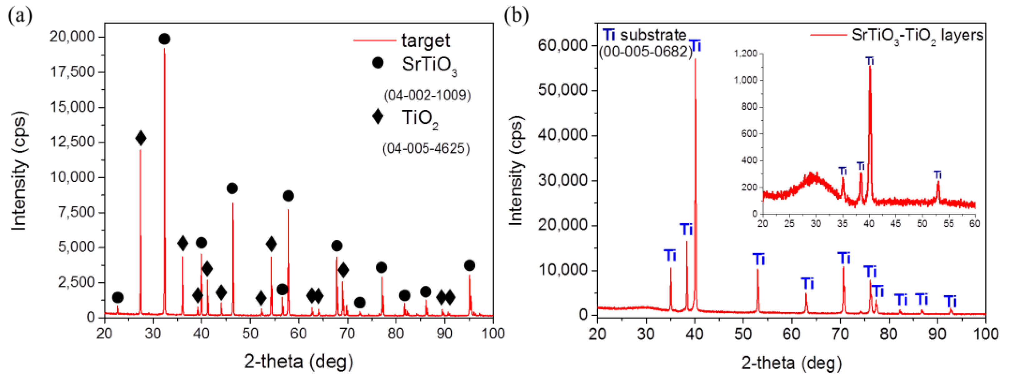
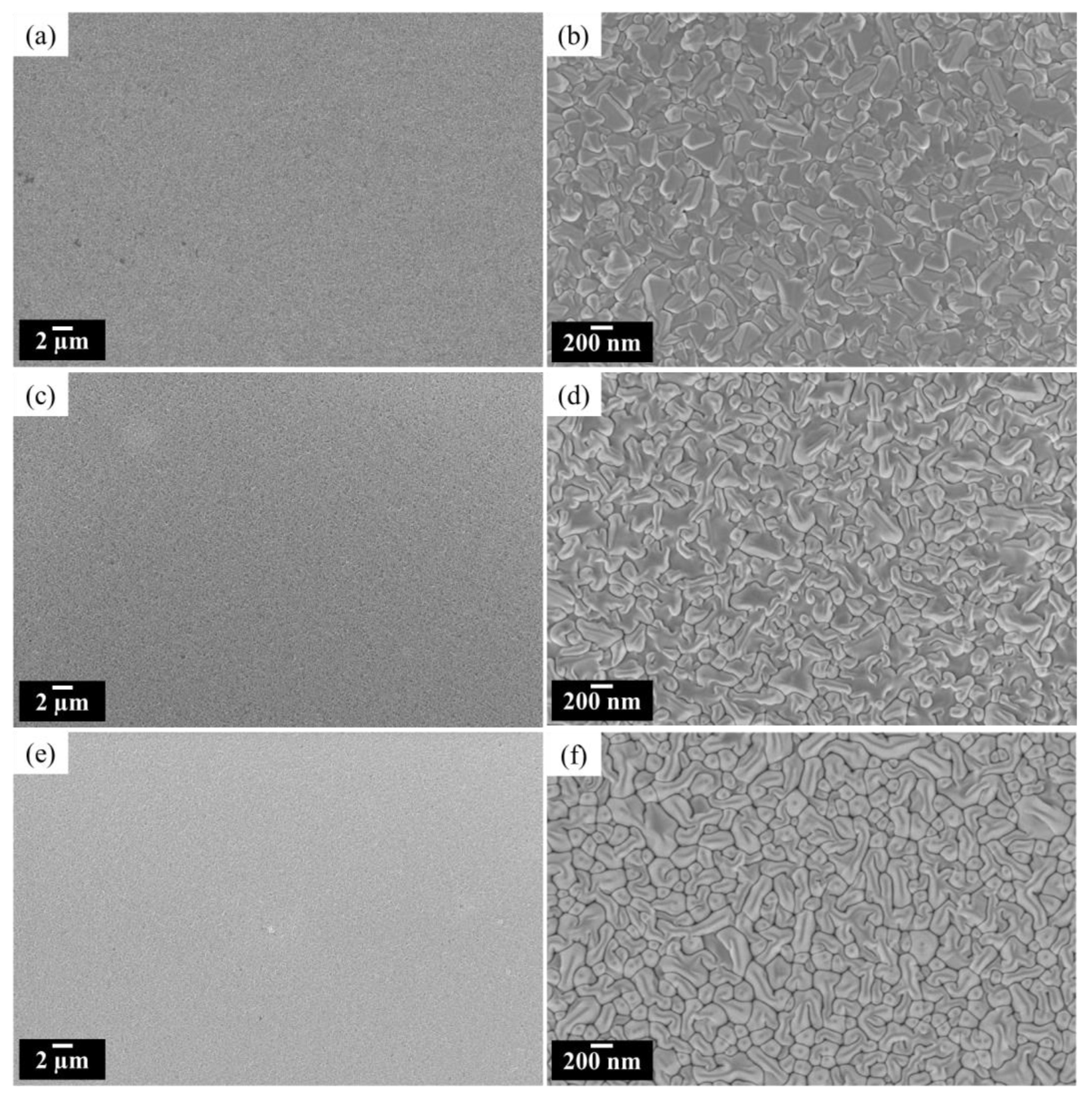
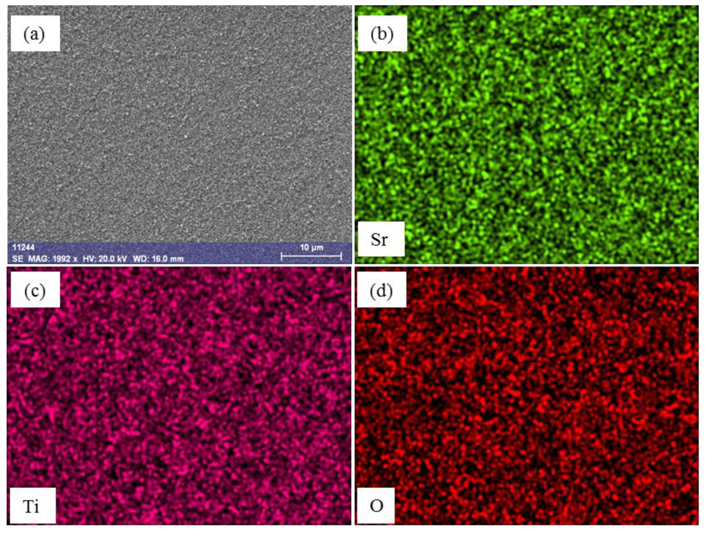
3.2. Material Characterization

Figure 2a shows the XRD patterns of the target prepared for sputtering. There were distinguished sharp peaks that can be attributed to the rutile (TiO2) phase and tausonite (SrTiO3) [20]. The sintering at 1300 °C/12 h in air allowed the synthesis of desired composition phases in the target. However, XRD patterns of SrTiO3-TiO2 layers deposited on the Ti substrate did not show corresponding peaks for constituent phases (Figure 2b). No evidence of the crystalline structure can indicate the amorphous nature of the deposited layers. The only recorded peaks were attributed to the Ti substrate. Additionally, the GIXD patterns (the inset of Figure 2b) show only weak reflection peaks attributed to the substrate. The rest indicates amorphous background. Similar results were registered for all deposited layer thicknesses regardless of the used substrate.
The SEM images presented in Figure 3 reveal the microstructure of the materials. In all investigated samples, the microstructure was homogeneous without any abnormal precipitates. In high-magnification pictures, it can be observed that with increasing sputtering time, the sharp edges between grains become smoother. The microstructure did not show the existence of split-ring resonators typical structures that like to form during the pulling of the SrTiO3-TiO2 eutectic crystals [7,13,29].
Good adhesion between FTO–glass substrate and deposited SrTiO3-TiO2 was confirmed for both 80- and 220-min sputtering times (Figure 4). In the case of the 12 min long sputtering, the recognition of a 50 nm thick layer was difficult.
The chemical composition of the obtained composite was examined by SEM equipped with an energy dispersive X-ray spectrometer (EDS) and presented in the form of maps for individual elements (Figure 5). The distribution of the key elements (Sr, Ti, and O) constituting the composite is homogeneous in the studied area. The presence of foreign inclusions was not registered.

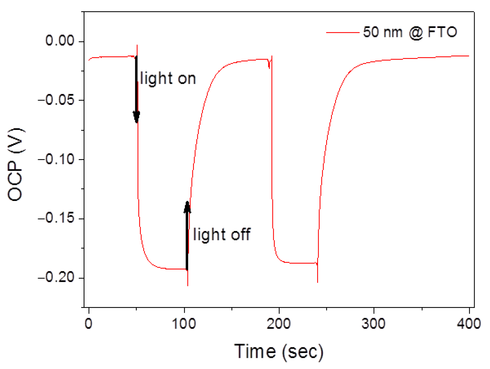
3.3. Photoelectrochemical (PEC) Measurements

PEC measurements were started with the registration of the open-circuit potential (OCP) over time when the light source is cyclically turned on and off (light on/off). Figure 6 shows that OCP for 50 nm thick layers on the FTO substrate has changed as a result of switching the light source on/off, indicating the photosensitivity of the tested material. The original OCP value of −13 mV is decreased to −192 mV under the light and then the original OCP is gradually recovered when the light is off. The decrease in OCP describes the n-type semiconductivity of the electrodes, which was registered for all tested electrodes. In the n-type semiconductors, the photogenerated holes flow to the surface-electrolyte interface where the oxygen evolution reaction takes place. The OCP shifts are in accordance with previous findings [4,30,31].
The photoelectrochemical analysis was continued through the current–voltage characteristics under alternating dark and illuminated conditions (so-called “chopped mode”). Despite the substrate, the lowest photocurrent densities were recorded for the thinnest layers. Figure 7 shows the effect of layer thickness on the photocurrent densities. An improvement in photoresponse was observed along with the decreasing thickness of the photoactive layer. The photocurrent densities were 11.8 × 10⁻³, 1.82 × 10⁻³ and 0.37 × 10⁻³ mAcm−2, successively for 50, 350 and 750 nm, at the potential of 1.2 V vs. SCE for layers deposited on Ti. This improvement can be explained by the relatively small grains: the photogenerated holes have enough time to diffuse to the interface with the electrolyte and to oxidize the water [12]. Additionally, the incident light is scattered at the grain boundaries, leading to enhanced optical absorption [32].
At the same time, the photocurrent densities recorded for electrodes on FTO substrates were lower at each deposition thickness in comparison with Ti ones. The differences between the observed photoresponses come from differences in the potential of the ohmic contact [11]. The conduction band levels for TiO2 and SrTiO3 are −4.21 and −4.24 eV, respectively [33], whereas the work function of polycrystalline titanium is 4.33 eV. The commonly cited value for work function for FTO is 4.40 eV [34]; however, as described by Helander et al. [35], it can be as high as 5.00 eV, as is found for commercial FTO. The higher mismatch between the conduction band and the work function can lead to the low photoresponse observed for FTO-based photoanodes.
The highest obtained photocurrent density of 11.8 × 10⁻³ mAcm−2 for 50 nm thick layers on Ti substrate was smaller than the reported 8.5 mAcm−2 for SrTiO3-TiO2 eutectic-based photoelectrodes [11]. The photoelectrochemical performance of our electrode is limited because of a lack of crystalline contact within the grain and between both phases. The amorphous nature of deposited layers increases recombination losses [36], diminishes charge-carrier transport [14] and worsens band gap and Fermi-level positions [37].
The investigation of changes in charge transfer resistance in the electrochemical impedance spectroscopy was carried out in dark and light conditions. The experimental data for EIS spectra presented in the Nyquist plots (Figure 7b,c) were fitted to the equivalent-circuit model, composed of two RC links [38]. The first RC link corresponding to the high-frequency region describes the resistance (Rsc) and capacitance (Csc) of the space charge zone. The second RC link at the low-frequency region describes charge transfer resistance (Rct) and the electric double-layer capacitance (Qdl). The fitting results are listed in Table 2. The photosensitivity of SrTiO3-TiO2 layers observed during OCP was confirmed by a strong decrease in Rct under illumination, regardless of the material thickness and substrate. Moreover, Rct was decreased with the thickness reaching the lowest value of 0.41 MΩ for 50 nm thick layers deposited on Ti. The comparison of substrates showed lower charge transfer resistances at each thickness for layers sputtered on the Ti substrate. EIS results are consistent with results from cyclic voltammetry.

4. Conclusions

The thin layers of SrTiO3-TiO2 composite material with a eutectic composition were successfully deposited on titanium and FTO substrates by sputtering. We were able to control the thickness of deposited layers by changing the sputtering parameters, such as the vacuum level, the voltage applied between the substrate and the target and the sputtering time. The deposited materials were found to be amorphous and homogeneous, both in terms of microstructure and composition. Material thicknesses of 50, 350 and 750 nm were achieved by carrying out the sputtering for 12, 80 and 220 min, respectively. These three-layer thicknesses were selected for the photoelectrochemical studies (OCP and chopped-CV). All prepared electrodes showed photoelectrochemical activity under a 150 W Xe-arc lamp with an irradiance intensity of 600 mWcm−2. The photocurrent densities were increasing while the thickness of the active layer was lowering, and the photocurrent density reached the highest value of 11.8 × 10⁻³ mAcm−2 at 1.2 V vs. SCE for a layer thickness of 50 nm. The highest values for photocurrents were recorded for SrTiO3-TiO2 sputtered on titanium substrates as a result of better matching of the work function with the conduction band. Further improvement in deposited layers is expected to lie in providing the full potential of eutectic composites by their high crystallinity, which allows matching the band gaps and the positions of band edges of constituent components and improving the photogenerated carriers transport ability. Thin layers of eutectic composites open up several unique opportunities: (a) manufacturing of hybrid materials, including complex oxides and oxide-non-oxide composite semiconductors with improved photoelectrochemical performance, (b) a better understanding of the behavior of highly crystalline semiconductor hetero-junctions formed in nanoscale multicomponent systems, and (c) a significant impact on areas beyond photoelectrochemistry such as nanotechnology, sensing, chemistry and photovoltaics.

Author Contributions

Conceptualization, methodology, investigation, project administration, and writing—original draft preparation, J.S.; methodology, investigation, writing—original draft preparation, K.K.; methodology, investigation, K.O.; methodology and investigation, M.G.; methodology, M.T.; conceptualization, methodology, writing—review and editing and supervision D.A.P. All authors have read and agreed to the published version of the manuscript.

Funding

The research has been supported by a SONATA Project (2016/23/D/ST5/02882) from the National Science Centre. The authors thank the ENSEMBLE3 Project carried within the Teaming for Excellence Horizon 2020 programme of the European Commission (GA No. 857543), and the International Research Agendas Programme (MAB/2020/14) of the Foundation for Polish Science co-financed by the European Union under the European Regional Development Fund and Teaming Horizon 2020 programme of the European Commission.

Institutional Review Board Statement

Not applicable.

Informed Consent Statement

Not applicable.

Data Availability Statement

Not applicable.

Conflicts of Interest

The authors declare no conflict of interest.

References

  1. Osterloh, F.E. Inorganic Materials as Catalysts for Photochemical Splitting of Water. Chem. Mater. 2008, 20, 35–54. [Google Scholar] [CrossRef]
  2. Rajeshwar, K. Fundamentals of Semiconductor Electrochemistry and Photoelectrochemistry; Encyclopedia of Electrochemistry; Viley-VCH Verlag: Hoboken, NJ, USA, 2002. [Google Scholar] [CrossRef]
  3. Currao, A. Photoelectrochemical Water Splitting. CHIMIA 2007, 61, 815–819. [Google Scholar] [CrossRef]
  4. Shao, J.; Wang, X.-T.; Xu, H.; Zhao, X.-D.; Niu, J.-M.; Zhang, Z.-D.; Huang, Y.-L.; Duan, J.-Z. Photoelectrochemical Performance of SnS2 Sensitized TiO2 Nanotube for Protection of 304 Stainless Steel. J. Electrochem. Soc. 2021, 168, 016511. [Google Scholar] [CrossRef]
  5. Llorca-Martínez, F.J.; Orera, V. Directionally solidified eutectic ceramic oxides. Prog. Mater. Sci. 2006, 51, 711–809. [Google Scholar] [CrossRef]
  6. Pawlak, D.A.; Kolodziejak, K.; Diduszko, R.; Rozniatowski, K.; Kaczkan, M.; Malinowski, M.; Kisielewski, J.; Lukasiewicz, T. The PrAlO3−Pr2O3 Eutectic, its Microstructure, Instability, and Luminescent Properties. Chem. Mater. 2007, 19, 2195–2202. [Google Scholar] [CrossRef]
  7. Pawlak, D.A.; Turczynski, S.; Gajc, M.; Kolodziejak, K.; Diduszko, R.; Rozniatowski, K.; Smalc, J.; Vendik, I. How Far Are We from Making Metamaterials by Self-Organization? The Microstructure of Highly Anisotropic Particles with an SRR-Like Geometry. Adv. Funct. Mater. 2010, 20, 1116–1124. [Google Scholar] [CrossRef]
  8. Gajc, M.; Surma, H.B.; Klos, A.; Sadecka, K.; Orlinski, K.; Nikolaenko, A.E.; Zdunek, K.; Pawlak, D.A. Nanoparticle Direct Doping: Novel Method for Manufacturing Three-Dimensional Bulk Plasmonic Nanocomposites. Adv. Funct. Mater. 2013, 23, 3443–3451. [Google Scholar] [CrossRef]
  9. Deska, R.; Sadecka, K.; Olesiak-Bańska, J.; Matczyszyn, K.; Pawlak, D.A.; Samoć, M. Nonlinear plasmonics in eutectic composites: Second harmonic generation and two-photon luminescence in a volumetric Bi2O3-Ag metamaterial. Appl. Phys. Lett. 2017, 110, 031102. [Google Scholar] [CrossRef]
  10. Myroshnychenko, V.; Stefanski, A.; Manjavacas, A.; Kafesaki, M.; Merino, R.I.; Orera, V.M.; Pawlak, D.A.; De Abajo, F.J.G. Interacting plasmon and phonon polaritons in aligned nano- and microwires. Opt. Express 2012, 20, 10879–10887. [Google Scholar] [CrossRef]
  11. Wysmulek, K.; Sar, J.; Osewski, P.; Orlinski, K.; Kolodziejak, K.; Trenczek-Zajac, A.; Radecka, M.; Pawlak, D.A. A SrTiO3-TiO2 eutectic composite as a stable photoanode material for photoelectrochemical hydrogen production. Appl. Catal. B Environ. 2017, 206, 538–546. [Google Scholar] [CrossRef]
  12. Kolodziejak, K.; Sar, J.; Wysmulek, K.; Osewski, P.; Warczak, M.; Sadkowski, A.; Radecka, M.; Pawlak, D.A. When eutectic composites meet photoelectrochemistry—Highly stable and efficient UV–visible hybrid photoanodes. J. Catal. 2017, 352, 93–101. [Google Scholar] [CrossRef]
  13. Bienkowski, K.; Turczynski, S.; Diduszko, R.; Gajc, M.; Gorecka, E.; Pawlak, D.A. Growth of a Plate-Shaped SrTiO3–TiO2 Eutectic. Cryst. Growth Des. 2011, 11, 3935–3940. [Google Scholar] [CrossRef]
  14. Feng, J.; Luo, W.; Fang, T.; Lv, H.; Wang, Z.; Gao, J.; Liu, W.; Yu, T.; Li, Z.; Zou, Z. Highly Photo-Responsive LaTiO2N Photoanodes by Improvement of Charge Carrier Transport among Film Particles. Adv. Funct. Mater. 2014, 24, 3535–3542. [Google Scholar] [CrossRef]
  15. Pinaud, B.A.; Vesborg, P.C.K.; Jaramillo, T.F. Effect of Film Morphology and Thickness on Charge Transport in Ta3N5/Ta Photoanodes for Solar Water Splitting. J. Phys. Chem. C 2012, 116, 15918–15924. [Google Scholar] [CrossRef]
  16. Scanlon, D.O.; Dunnill, C.W.; Buckeridge, J.; Shevlin, S.A.; Logsdail, A.J.; Woodley, S.M.; Catlow, C.R.A.; Powell, M.J.; Palgrave, R.G.; Parkin, I.P.; et al. Band alignment of rutile and anatase TiO2. Nat. Mater. 2013, 12, 798–801. [Google Scholar] [CrossRef]
  17. Zhou, N.; Chen, G.; Xian, H.; Zhang, H. Synthesis of SrO(SrTiO3)n (n = 1, 2, ∞) compounds and electronic structure analysis. Mater. Res. Bull. 2008, 43, 2554–2562. [Google Scholar] [CrossRef]
  18. Zhang, J.; Bang, J.H.; Tang, C.; Kamat, P.V. Tailored TiO2−SrTiO3 Heterostructure Nanotube Arrays for Improved Photoelectrochemical Performance. ACS Nano 2010, 4, 387–395. [Google Scholar] [CrossRef]
  19. Baek, J.-Y.; Duy, L.T.; Lee, S.Y.; Seo, H. Aluminum doping for optimization of ultrathin and high-k dielectric layer based on SrTiO3. J. Mater. Sci. Technol. 2020, 42, 28–37. [Google Scholar] [CrossRef]
  20. Gillispie, M.A.; van Hest, M.F.A.M.; Dabney, M.S.; Perkins, J.D.; Ginley, D.S. rf magnetron sputter deposition of transparent conducting Nb-doped TiO2 films on SrTiO3. J. Appl. Phys. 2007, 101, 033125. [Google Scholar] [CrossRef]
  21. Jabbar, S.; Ahmad, R.; Chu, P.K. Morphological and electrical properties of SrTiO3/TiO2/SrTiO3 sandwich structures prepared by plasma sputtering. Chin. Phys. B 2017, 26, 10702. [Google Scholar] [CrossRef]
  22. Shang, Q.; Yu, T.; Tan, X.; Zhang, Z.; Zou, Y.; Zhang, L.; Zhang, Y.; Wang, S. Enhanced photoelectrochemical performance of {001}TiO2/{001}SrTiO3 epitaxial heterostructures. J. Solid State Electrochem. 2016, 20, 123–132. [Google Scholar] [CrossRef]
  23. Rahman, M.Y.A.; Samsuri, S.A.M.; Umar, A.A. TiO2–SrTiO3 composite photoanode: Effect of strontium precursor concentration on the performance of dye-sensitized solar cells. Appl. Phys. A 2019, 125, 59. [Google Scholar] [CrossRef]
  24. Ruzimuradov, O.; Sharipov, K.; Yarbekov, A.; Saidov, K.; Hojamberdiev, M.; Prasad, R.M.; Cherkashinin, G.; Riedel, R. A facile preparation of dual-phase nitrogen-doped TiO2–SrTiO3 macroporous monolithic photocatalyst for organic dye photodegradation under visible light. J. Eur. Ceram. Soc. 2015, 35, 1815–1821. [Google Scholar] [CrossRef]
  25. Zhu, X.; Gu, P.; Wu, H.; Yang, D.; Sun, H.; Wangyang, P.; Li, J.; Tian, H. Influence of substrate on structural, morphological and optical properties of TiO2thin films deposited by reaction magnetron sputtering. AIP Adv. 2017, 7, 125326. [Google Scholar] [CrossRef] [Green Version]
  26. Huerta-Flores, A.M.; Usiobo, O.J.; Audinot, J.-N.; Heyberger, R.; Choquet, P.; Boscher, N.D. Low Temperature Open-Air Plasma Deposition of SrTiO3 Films for Solar Energy Harvesting: Impact of Precursors on the Properties and Performances. ACS Appl. Mater. Interfaces 2022, 14, 8527–8536. [Google Scholar] [CrossRef]
  27. Roy, R.; (Pennsylvania State University, University Park: College Township, PA, USA). Private communication, 1957.
  28. The International Centre for Diffraction Data USA. 2012. Available online: www.icdd.com (accessed on 9 September 2022).
  29. Ramírez, M.O.; Molina, P.; Mateos, L.; Turczyński, S.; Kaczkan, M.; Malinowski, M.; Pawlak, D.A.; E Bausa, L. Pr3+-Based Fluorescent TiO2 Split Ring Resonator-like Crystalline Microstructures. Sci. Adv. Mater. 2013, 5, 921–926. [Google Scholar] [CrossRef]
  30. Yang, Y.; Cheng, Y.F. Factors Affecting the Performance and Applicability of SrTiO3Photoelectrodes for Photoinduced Cathodic Protection. J. Electrochem. Soc. 2017, 164, C1067–C1075. [Google Scholar] [CrossRef]
  31. Si, Y.; Liu, H.; Yu, H.; Jiang, X.; Sun, D. A heterogeneous TiO2/SrTiO3 coating on titanium alloy with excellent photocatalytic antibacterial, osteogenesis and tribocorrosion properties. Surf. Coat. Technol. 2022, 431, 128008. [Google Scholar] [CrossRef]
  32. Kwong, W.L.; Savvides, N.; Sorrell, C. Electrodeposited nanostructured WO3 thin films for photoelectrochemical applications. Electrochim. Acta 2012, 75, 371–380. [Google Scholar] [CrossRef]
  33. Li, J.; Wu, N. Semiconductor-based photocatalysts and photoelectrochemical cells for solar fuel generation: A review. Catal. Sci. Technol. 2015, 5, 1360–1384. [Google Scholar] [CrossRef]
  34. Shang, D.S.; Shi, L.; Sun, J.R.; Shen, B.G.; Zhuge, F.; Li, R.W.; Zhao, Y.G. Improvement of reproducible resistance switching in polycrystalline tungsten oxide films by in situ oxygen annealing. Appl. Phys. Lett. 2010, 96, 072103. [Google Scholar] [CrossRef] [Green Version]
  35. Helander, M.G.; Greiner, M.T.; Wang, Z.B.; Tang, W.M.; Lu, Z.H. Work function of fluorine doped tin oxide. J. Vac. Sci. Technol. A 2011, 29, 011019. [Google Scholar] [CrossRef]
  36. Maeda, K.; Terashima, H.; Kase, K.; Higashi, M.; Tabata, M.; Domen, K. Surface Modification of TaON with Monoclinic ZrO2 to Produce a Composite Photocatalyst with Enhanced Hydrogen Evolution Activity under Visible Light. Bull. Chem. Soc. Jpn. 2008, 81, 927–937. [Google Scholar] [CrossRef] [Green Version]
  37. Chen, Z.; Deutsch, T.G.; Dinh, H.N.; Domen, K.; Emery, K.; Forman, A.J.; Gaillard, N.; Garland, R.; Heske, C.; Jaramillo, T.F. Experimental Considerations. In Photoelectrochemical Water Splitting; Springer: Berlin/Heidelberg, Germany, 2013; pp. 17–44. [Google Scholar]
  38. Lopes, T.; Andrade, L.; Le Formal, F.; Gratzel, M.; Sivula, K.; Mendes, A. Hematite photoelectrodes for water splitting: Evaluation of the role of film thickness by impedance spectroscopy. Phys. Chem. Chem. Phys. 2014, 16, 16515–16523. [Google Scholar] [CrossRef] [PubMed]
Figure 1. Thickness of the layers measured by profilometry: (a) relationship between thickness of the layer and sputtering time; height of the layer measured after (b) 12 min, (c) 80 min and (d) 220 min of sputtering.
Coatings 12 01876 g001
Figure 2. X-ray diffraction of (a) prepared target for sputtering revealing SrTiO3 and TiO2 phases and (b) SrTiO3-TiO2 layers deposited on Ti substrate with the 220 min long sputtering process. The inset represents GIXD patterns focused on 2-theta range of 20–60 deg. The XRD card numbers were put in the brackets for SrTiO3, TiO2 and Ti.
Coatings 12 01876 g002
Figure 3. SEM images of the SrTiO3-TiO2 layers after sputtering for (a,b) 12 min; (c,d) 80 min; and (e,f) 220 min.
Coatings 12 01876 g003
Figure 4. SEM picture made on cross-section of SrTiO3-TiO2 after sputtering for (a) 80 min and (b) 220 min.
Coatings 12 01876 g004
Figure 5. SEM photo with EDS analysis taken for 350 nm SrTiO3-TiO2 at FTO: (a) SEM photo at 1992× magnification; EDS mapping of (b) Sr, (c) Ti and (d) O elements.
Coatings 12 01876 g005
Figure 6. Changes in the open-circuit potentials over time when turning the light source on and off.
Coatings 12 01876 g006
Figure 7. The influence of layer thickness on the obtained photocurrent densities presented in chopped current–voltage curves for layers deposited on (a) Ti substrate and (b) FTO substrate. The influence of layer thickness under illumination on electrochemical impedance spectroscopy is presented in Nyquist plots for layers deposited on (c) Ti substrate and (d) FTO substrate.
Coatings 12 01876 g007
Table 1. List of the deposition parameters: PAr vacuum level expressed in argon pressure, power of the device, target to substrate distance, sputtering time and the measured thickness of the layer.
PAr (hPa)Power (W)Target to Substrate Distance (mm)Sputtering Time (min)Thickness (nm)
2 × 10−2400431240–60
2 × 10−24004360220–250
2 × 10−24004380330–360
2 × 10−240043100450–480
2 × 10−240043150580–620
2 × 10−240043220720–770
Table 2. The fitting results of the experimental data for the proposed equivalent-circuit model for SrTiO3-TiO2 layers sputtered on Ti substrate and FTO substrate under dark and light conditions: where Rs is series resistance, Rsc is space charge resistance, Csc is space charge capacitance, Rct is charge transfer resistance, Qdl is electrode capacitance in constant phase element, and n is constant phase exponent.
SrTiO3-TiO2 @ FTO
Thickness (nm) Rs (Ω)Rsc (Ω)Csc (F)Rct (MΩ)Qdl (F s(n − 1))n
750Dark30.075.33.51 × 10−923.21.21 × 10−80.95
750Light29.874.43.57 × 10−910.51.23 × 10−80.95
350Dark23.584.53.88 × 10−953.11.94 × 10−80.98
350Light23.082.93.85 × 10−94.292.05 × 10−80.98
50Dark28.999.83.48 × 10−911.02.87 × 10−70.96
50Light22.0102.03.01 × 10−91.604.71 × 10−70.91
Publisher’s Note: MDPI stays neutral with regard to jurisdictional claims in published maps and institutional affiliations.

