Article

Simulated Performance of a Broadband Solar Absorber Composed of Sectioned Au Disk Structures and ZnS/Au Thin Layers

1
Department of Environment and Resource, Tianfu Institute of Research and Innovation, School of National Defense & Nuclear Science and Technology, Southwest University of Science and Technology, Mianyang 610059, China
2
College of Physics and Electronics, Central South University, Changsha 410083, China
*
Author to whom correspondence should be addressed.
These authors contributed equally to this work.
Coatings 2022, 12(12), 1863; https://doi.org/10.3390/coatings12121863
Submission received: 25 October 2022 / Revised: 25 November 2022 / Accepted: 28 November 2022 / Published: 30 November 2022
(This article belongs to the Special Issue Micro-Nano Optics and Its Applications)

Abstract

:
Solar energy is considered an essential source of energy because of cleanliness and ubiquity. However, how to effectively absorb solar energy within the range of solar radiation is an urgent problem to be solved. The design of high-performance broadband perfect absorbers is an important way to collect solar energy efficiently. In this paper, we propose a novel broadband solar energy absorber based on zinc sulfide (ZnS). It is a three-layer (Au-ZnS-Au) structure with new types of sectioned disks employed in the top layer. The sectioned disks can enhance the absorption efficiency. Surface plasmon polariton (SPP) and electric dipole resonance increase the absorption of light, so the proposed absorber can achieve broadband perfect absorption. Simulation by a finite element analysis (COMSOL) method shows that absorption with a bandwidth of 354 THz from 430 THz–784 THz has been achieved, and the average absorption is 95%. This indicates that the perfect absorption range of the proposed absorber is 78.7% of the visible range. The perfect absorber has four perfect absorption peaks, which can reach a maximum absorption rate of 99.9%. In addition, our absorber is polarization insensitive due to the design of the rotational symmetry structure of the sectioned disks. The absorber is composed of refractory metals so that it can work under actual solar radiation and high-temperature conditions. The proposed solar energy absorber is important for many applications such as solar cells, thermal photovoltaic technology, and sensing.

1. Introduction

Solar energy is regarded as an indispensable source of energy because of its abundant reserves, cleanliness, and universality. How to absorb solar energy efficiently and make it available to humankind is a very significant topic [1,2,3]. Using a perfectly designed broadband absorber with excellent performance is a key way to collect solar energy efficiently [4,5].
The perfect absorber is an electromagnetic resonator that absorbs nearly 100% of solar energy. By choosing the proper material to design the structure, the electromagnetic component of the incident electromagnetic wave is coupled so that the sunlight incident on the absorber surface is completely absorbed without reflection or transmission [6]. In 2008, the first study of a metamaterial absorber by Landy et al. achieved an absorption rate of 96%, kicking off the quest for the perfect absorber [7]. Perfect absorbers typically only achieve perfect absorption at specific frequencies [8,9]. To collect solar energy efficiently, the bandwidth of the absorber needs to be extended so that it can absorb as much solar energy as possible in the frequency range where the Earth receives solar radiation (380 THz–850 THz). In 2020, Peiqi Yu et al. proposed an ultra-broadband solar absorber based on refractory titanium metal that could have an absorption efficiency of more than 90% in an ultra-broadband of 1759 nm [10].
The study of broadband perfect absorbers has two main aspects. On the one hand, the selection of suitable materials is a significant method to create perfect absorbers. Under electromagnetic wave irradiation in the visible and near-infrared wavelengths, the dielectric constants of precious metals such as Au and silver are complex, and the absolute value of the real part is much larger than that of the imaginary part. After calculations, it can be learned that electromagnetic waves propagate mainly on the surface of the metal and decay rapidly in the direction of the perpendicular metal surface in an exponential form [6]. This transverse magnetic wave traveling along the interface is called surface plasmon polariton (SPP). A perfect absorber made of precious metals such as Au can block the transmission of sunlight to form equipolar excitations on the metal surface and enhance the absorption of solar energy. However, traditional metallic materials have disadvantages such as low melting points and poor structural stability, so attention has also been paid to high-melting-point materials such as nickel and titanium [11,12,13,14].
The other aspect is the design of a reasonable nanostructure for a broadband perfect absorber, which is also key to achieving broadband absorption [15,16,17]. A combination of multiple resonators within a resonant unit allows multiple absorption peaks for the absorber. Resonant absorber peaks are coupled to each other so that the absorption capacity of the frequency range between the different absorber peaks is increased. This is a classical method of extending the absorption bandwidth [18,19,20,21]. A perfect absorber designed by Yubin Zhang et al. with a square array structure made of ancient Chinese coin shapes obtained two absorption rates up to 99.9% of the perfect absorption peaks, but it constituted a double-frequency narrow-band absorption [22]. In contrast, Zao Yi et al. designed a perfect absorber with a four-layer annular disc structure that achieved absorption efficiencies of 99.1%, 99.8%, and 99.8% at wavelengths of 474 nm, 735 nm, and 1834 nm, respectively. This absorber had an absorption rate higher than 90% in the wavelength range of 420 nm–1950 nm [23].
In this paper, we propose a novel broadband solar energy absorber based on zinc sulfide (ZnS). It is a three-layer (Au-ZnS-Au) structure with an array of four sectioned disks and a square employed in the top layer. The broadband absorption of solar radiation is achieved with an average of 95% continuous absorption at 430 THz–784 THz and a bandwidth up to 354 THz. The broadband absorption rate of solar radiation is achieved. It also achieves a very high absorption rate greater than 99% in the 438 THz–478 THz range. It has four perfect absorption peaks, with absorption efficiencies of 99.941%, 99.424%, 99.116%, and 99.325% at frequencies of 449 THz, 493 THz, 651 THz, and 743 THz, respectively. In this paper, a metal-dielectric-metal (MIM) structure is adopted [24,25,26]. Au and ZnS are selected as the materials, which have a high melting point and stable chemical properties and can also maintain a stable structure and function normally in complex electromagnetic environments such as outdoor strong solar radiation [27,28,29]. Structurally, due to its rotational symmetry structural design, the absorption spectrum of this absorber is insensitive to polarization and maintains a high absorption rate in a polarized light environment. The simulation of broadband absorption is carried out by means of finite element analysis (COMSOL). The optimal structural parameters are found through our investigation based on the influence of different structures on the efficiency of the absorber.
These designs make the absorbers proposed in this paper have profound significance for further theoretical research and practical application. This paper describes the effect of the change of the top layer structure of the absorber on the absorption efficiency, which provides a theoretical reference for the design of other similar solar absorbers. In actual production, the absorber is easy to fabricate due to its 3-layer structure and disks arrays. The data show that it has good process tolerance because it can maintain high absorption when the parameters change. The absorption spectrum of solar radiation is given in this paper, which shows the excellent absorption performance of the solar absorber under practical conditions. The high-temperature-resistant material and polarization-insensitive feature enable the absorber to work in the high-temperature and complex environment of real sunlight. This indicates that our broadband perfect absorber has a wide range of applications and has great potential for applications in solar cells, sensing, thermal photovoltaic technology, photocatalysis, solar power tower systems, etc. [30,31,32,33].

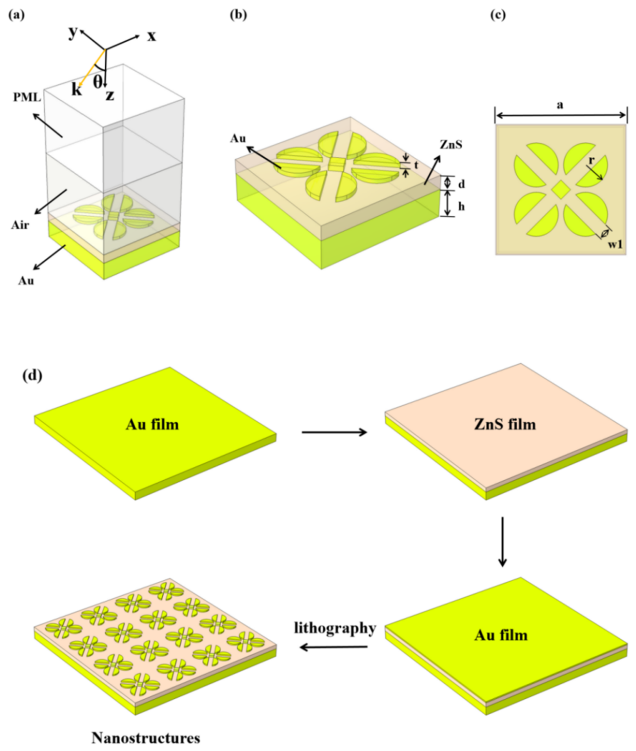
2. Structure and Method

The structure proposed in this paper is shown in Figure 1, where the cell structure of the absorber is periodically repeated in the XY plane. We achieve this infinite array arrangement by setting periodic boundary conditions in the x- and y-directions and by setting a perfectly matched layer (PML) in the z-direction. Each periodic small cell of the absorber consists of a three-layer structure, which is a metal-dielectric-metal absorber (MDM) [34]. The top layer consists of an array of deformed disks made of Au of thickness t, which can suppress electromagnetic reflection. The structure of the absorber material is designed so that the equivalent impedance of the absorber matches the impedance of free space at a specific frequency. Then, electromagnetic waves at that frequency are not reflected by this metamaterial but are completely absorbed by the absorber [15]. The structure of the sectioned disks consists of four circles of radius r arranged equidistantly in a 2 × 2 format, with slots of width w1 in each disk along the diagonal of the array, leaving a square of side length w1 in the center of the four disks. Varying these parameters, adjusting the shape and size of the top layer of metal, can modulate the coupling of the electric field of the incident electromagnetic waves. The middle layer uses the semiconductor material ZnS as a dielectric layer with a thickness of d. Varying the type and thickness of the dielectric layer modulates the coupling of the magnetic field of the incident electromagnetic waves [6]. The bottom layer is a Au substrate of thickness h, which is used to block the transmission of electromagnetic waves.
In order to verify whether the absorber proposed in this paper has a perfect absorption effect, we use the COMSOL simulation platform. The finite element method based on the COMSOL simulation platform is used to investigate the performance of the designed metamaterial structure by conducting simulation experiments [35]. In fact, a series of fluctuating equations in the transmission of electromagnetic waves are converted into a discrete system of linear algebraic equations to calculate them [36]. Finally, we optimize the metamaterial absorber with the following parameters for the optimal nanostructure: a radius of sectioned disks r = 109 nm, a width of the slit between sectioned disks w1 = 5 nm, the thickness of a ZnS absorption layer d = 66 nm, and the thickness of a surface Au absorption layer t = 25 nm. The corresponding detailed parameters are shown in Table 1.

3. Results and Discussion
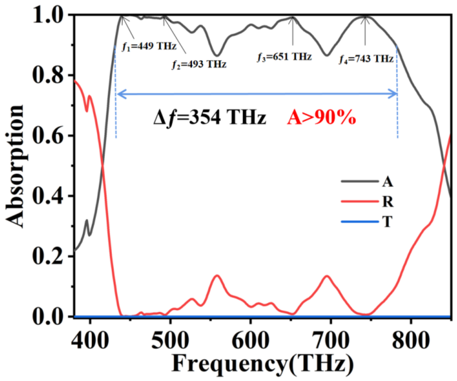
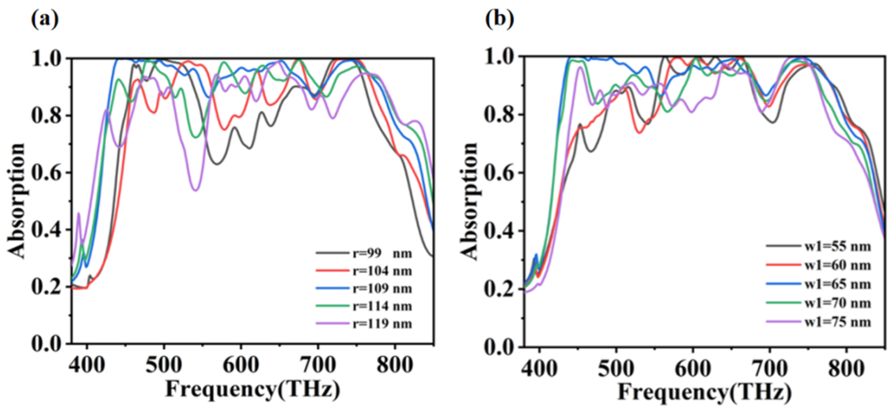
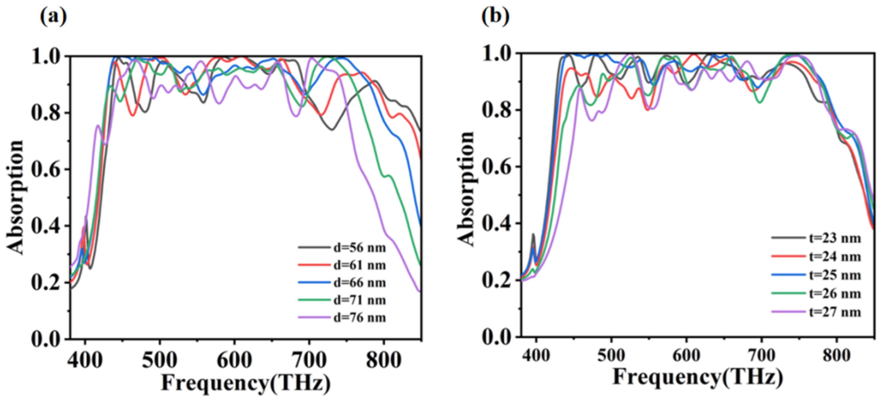
3.1. Results

The absorber perfectly absorbs in the broad band and is also polarization insensitive. In addition to this, the absorber is able to operate under realistic solar radiation and high-temperature conditions. These features will give our design the potential for a wide range of applications. The individual features are described in detail below.
Figure 2 plots the absorption spectrum of the broadband perfect absorber proposed in this paper with a vertically incident TE wave (transverse electric wave), where A is the absorption of the designed absorber, R is the reflection, and T is the transmission. We can observe four perfect absorption peaks at frequencies of 449 THz, 493 THz, 651 THz, and 743 THz, with absorption efficiencies of 99.941%, 99.424%, 99.116%, and 99.325%, respectively. The perfect absorption peak ƒ1 and the perfect absorption peak ƒ2 in the low-frequency region form a very high absorption region with an absorption rate higher than 99%. It has an average absorbance of 99.2% and a bandwidth of 40 THz. The entire broadband perfect absorber achieves an average of 95% continuous absorption at 430 THz–784 THz with a bandwidth of up to 354 THz, with an observable solar radiation spectrum on Earth ranging from approximately 380 THz–850 THz with a bandwidth of 470 THz. This indicates that the perfect absorption range of the proposed absorber is 78.7% of the visible range. Our absorber has a broad absorption spectrum for sunlight and is able to fully absorb solar energy.
Compared to works of other researchers, as shown in Table 2, our design of a broadband perfect absorber based on a sectioned disk structure has a high absorption rate and a very wide absorption bandwidth [35,37,38,39]. It has excellent performance. In addition, for absorbers with similar absorption rates, the absorber proposed in this paper has a wider bandwidth.

3.2. Polarization Sensitivity

A practical and ideal perfect absorber also requires polarization-independent absorption [40,41,42]. We simulated absorption curves for different polarization modes. It can be seen that the absorptance curve of the absorber does not change when the incident light changes from a transverse electric wave (TE wave) to a transverse magnetic wave (TM wave), as shown in Figure 3 and has a high absorption of 95% on average over the frequency range 430 THz–784 THz. Therefore, the absorber is a polarization-insensitive structure. This allows our absorber to continue to ensure high absorbance even under changing polarization states, such as solar irradiation, and can be used for better applications in solar absorbers, photocatalysis, sensing, etc. [43,44,45,46]. The polarization insensitivity of the absorber is due to the design of its rotationally symmetrical structure. Each unit is four disks arranged in an array of two rows and two columns and is slotted diagonally. This structure ensures that the shape of the absorber layer is the same for any polarization state.

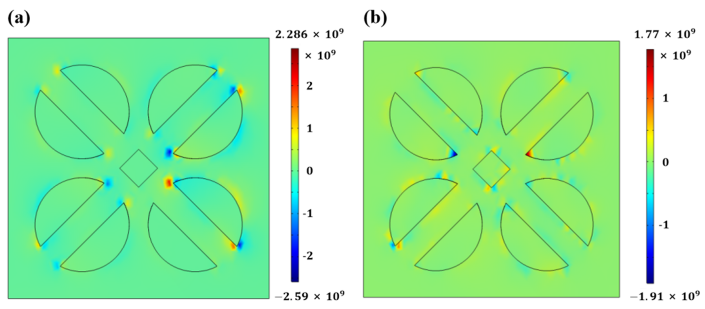
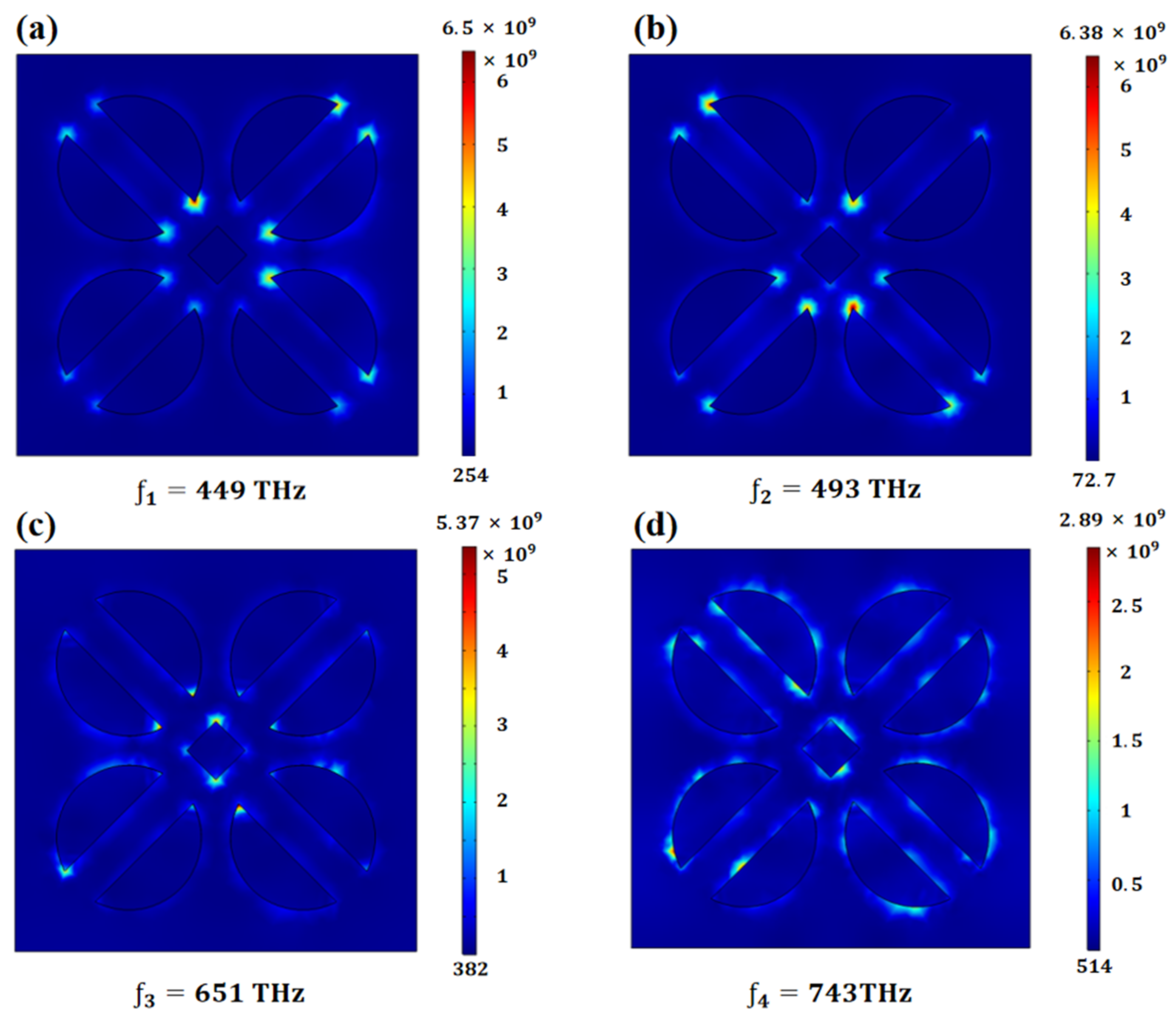
3.3. Separation and Electric Fields
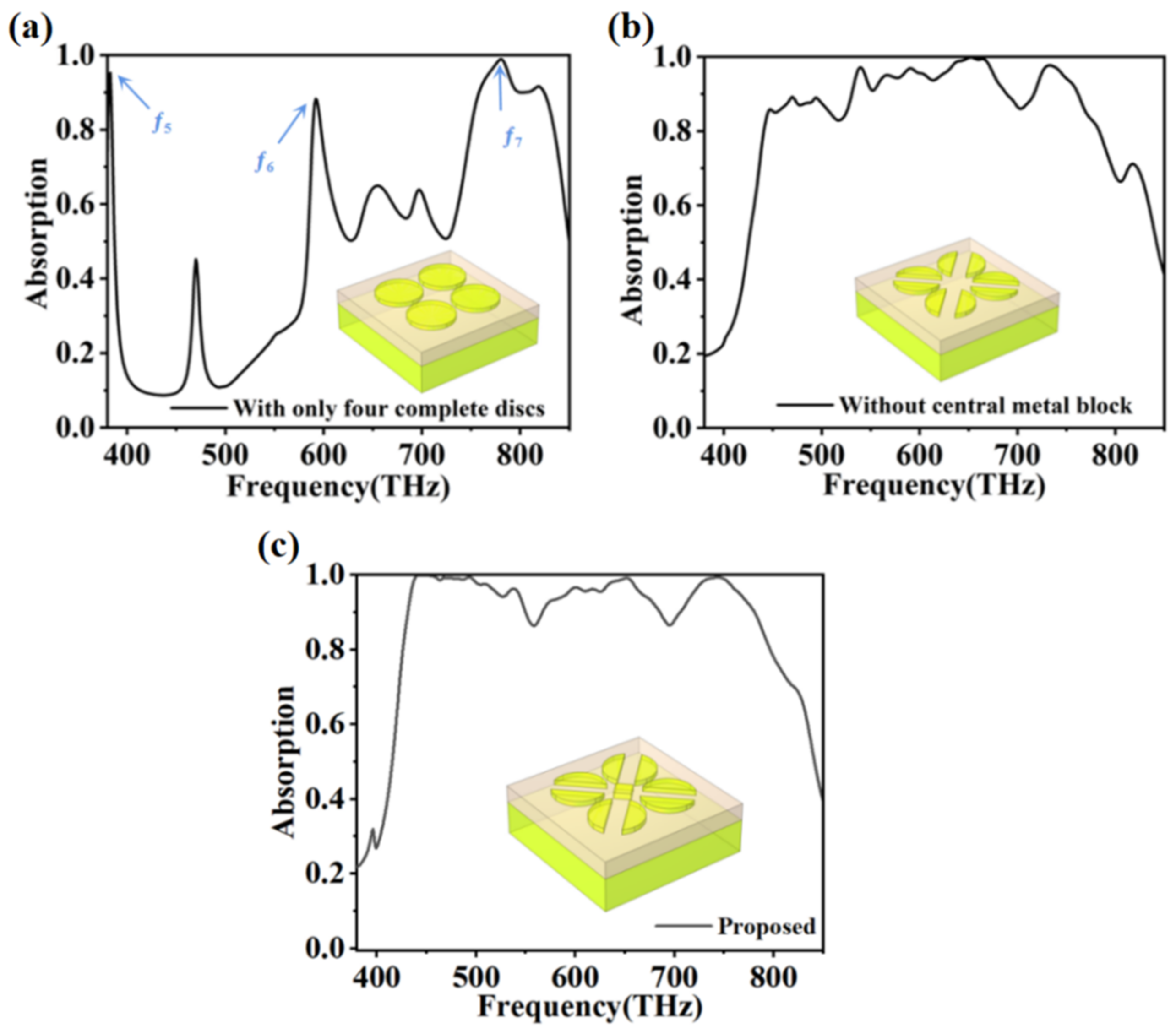
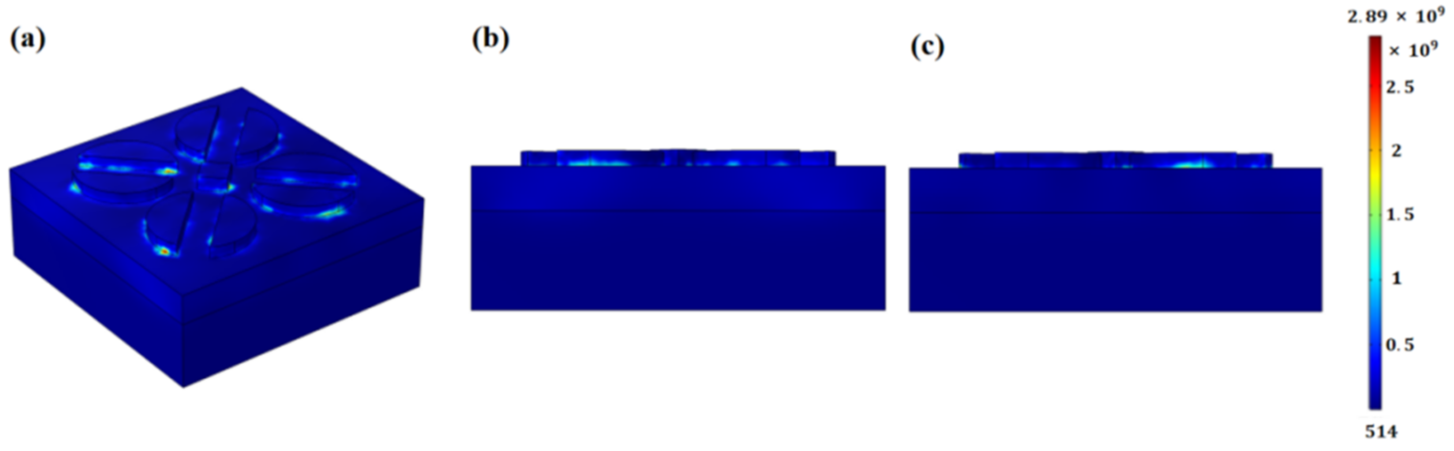
In order to better explain the absorption principle of the broadband perfect absorber, we will explore the proposed absorber step by step. Firstly, the absorption curve of the absorber with only four complete disks is shown in Figure 4a. We can see that the disc-only array structure has a good absorption effect only in the high-frequency region. Absorption peaks f5, f6, and f7 formed in the low-frequency, middle-frequency, and high-frequency regions, respectively. However, the three absorption peaks are far apart from each other, which does not allow effective resonance and perfect broadband absorption. After our innovative diagonal slotting of the disc, we can see from Figure 4b that the absorption between the original absorption peaks is significantly higher, the absorption capacity of the sectioned disk structure is considerably higher, and the high absorption bandwidth is significantly increased, resulting in broadband absorption [47]. This is due to the effective resonant absorption provided by the plasma resonance between the semicircles after the splitting of the overall disc into two semicircles, which also creates a complementary spectral absorption response [48]. However, the average absorption is not high enough in the absorption range. With the addition of the center square, a significant increase in absorption is clearly observed in the low-frequency region, and a very high absorption zone higher than 99% in the 449 THz–493 THz range is formed. The center square increases the overall absorptance of the absorber, making it a very effective broadband perfect absorber.
To explore the absorption mechanism in depth, we plotted the electric field distribution Ex at the low-frequency absorption peak f2 and the high-frequency absorption peak f3 against the electric field distribution E at each absorption peak frequency. From Figure 5a, we observe that opposite charges accumulate at the corners of the sectioned disks, resulting in the production of multiple pairs of electric dipoles [49]. At the same time, the opposite charges are distributed on the rounded edges of the adjacent disks, but the number of charges is smaller compared to the angles. That is, electric dipoles are also formed on the adjacent disks. The strong electric dipoles excite electric dipole resonance, which consumes the incident electromagnetic waves and ultimately results in high absorption [50,51,52]. This also explains why intact disks have low absorption at low frequencies, while our sectioned disks with slots in them can have high absorption at low frequencies [53]. In the high-frequency state, the number of charges at the corners of the sectioned disks decreases, the number of electric dipoles decreases, and the electric field strength decreases. However, two pairs of electric dipoles are formed on either side of the central square, and more pairs of less intense electric dipoles are formed on the same curved edge of the same disk. Therefore, the absorber still maintains a high absorption rate.
Observing the change in the electric field distribution at the four peaks from low to high frequencies in Figure 6, we can see that the frequency changes from f1 (449 THz) to f2 (491 THz) in the low-frequency state, the charge aggregation remains the same, the change in the number of charges is also smaller, and the distribution of charges shifts with a clockwise trend. The electric dipoles are still distributed in a rotationally symmetrical manner at the corners of the sectioned disks and do not decrease in number or intensity. This explains why the absorption rate exceeds 99% in the very high absorption zone between the f1 absorption peak and the f2 absorption peak; during the change in frequency from f1 to f2, the electric field distribution only rotates, the number and intensity of the electric dipoles do not change, and the resonance generated by the whole absorber changes very little, so the loss rate of the incident electromagnetic wave remains at a high level [54,55].
When changing to the high-frequency region, as shown in Figure 6d, the charge is no longer concentrated at the corners and the electric field is distributed on each edge of the sectioned disks. Combining the axonometric, front, and side views of the absorber’s electric field distribution in Figure 7, we find that the electric field is only distributed at the interface between the metal absorber layer and the ZnS dielectric layer. This indicates that the incident electromagnetic wave forms surface plasmon polariton (SPP) at the metal-dielectric interface of the absorber [56]. This is because our absorber layer material, Au, has a complex dielectric constant in the visible and near-infrared wavelengths, with the real part being negative and much larger in absolute value than the imaginary part. That means ε m = ε r + i ε i and ε r ε i , where ε m represents the permittivity of a metal, ε r represents the real part of ε m , and ε i represents the imaginary part. The distribution functions of the electric fields E r , t and magnetic fields B r , t can be derived from Maxwell’s set of equations as follows [57,58,59,60].
E r , t = ( i k α ) E dx e i ( kx + α z ω t )   z 0 ( i k β ) E dx e i kx + β z ω t   z 0
B r , t = ε d ω α c 2 E dx e i kx + α z ω t j   z 0 ε m ω c 2 β E dx e i kx + β z ω t j   z 0
k = ω c ε d ε m ε d + ε m
α = ω c ε d 2 ε d + ε m
β = ω c ε m 2 ε d + ε m
where ε d represents the dielectric constant of the medium, and ε m represents the dielectric constant of the metal. α, β are the wave vectors of vertical direction (Z axis) of the electromagnetic wave in a transparent medium and metal, and k is the wave vector of the electromagnetic wave in a horizontal plane (XY plane). The Au absorber layer satisfies ε m = ε r + i ε i , ε r ε i and ε r < 0 , so α , β quickly decay. Electromagnetic waves attenuate rapidly along with the vertical metal-medium interface, leaving only SPP propagating along with the interface, as shown in Figure 7. In the high-frequency region, the wavelength of electromagnetic waves is short, the dielectric layer skinning depth is shallow, but the ohmic loss of the metal layer is large. The SPP mode makes the incident electromagnetic waves undergo great loss, and the electric field is difficult to penetrate below the dielectric layer, so the incident light is perfectly absorbed.

3.4. Structure

In order to study the influence of different structural parameters on the absorber and to consider the errors in process production, changes are made to the individual parameters of this broadband absorber. The structure of the top deformation disk of the broadband absorber proposed in this paper is determined by two parameters: the disk radius r and the slot width w1.
In Figure 8, the blue line r = 109 nm is the final optimum parameter chosen in this paper. The other colored lines reflect the effect on the resonant absorber when the parameter is increased or decreased. It can be seen from Figure 8a that as the radius of the disk r decreases, the absorption peak f1 redshifts and the absorption efficiency decreases. The high absorption region (with a bandwidth of 44 THz) between the absorption peak f1 and the absorption peak f2 shows a decrease in absorption. Absorption peak f3 also shows a purple shift or a decrease in absorption efficiency. Absorption peaks f2 and f3 fluctuate in absorption in the band with a large absorption rate and a low absorption rate. However, near the fourth absorption peak (719 THz–746 THz), an extremely high absorption region with an absorption rate higher than 99% and a bandwidth of 27 THz formed. The reason for these phenomena is that the area of the disk will change greatly when the radius of the disk changes [61]. The absorption peaks formed in the topmost Au arrays vary with the plasmon resonance. Our final choice of broadband absorber has a very high absorption region higher than 99% at 44 THz because there are two perfect absorption peaks in close proximity: the f1 absorption peak at 449 THz with 99.941% absorption and the f2 absorption peak at 493 THz with 99.424% absorption. The two absorption peaks are coupled to each other, ultimately giving an absorbance of more than 99% in the region between the two absorption peaks. After changing the parameters, the frequency and absorbance of the f1 absorption peak changed, so did the coupling, so the absorbance of the absorption region between the peaks changed and did not fully achieve high absorption. Although a period of very high absorption was also produced when the disk radius r was reduced, the r = 109 nm parameter was chosen to maintain a more stable absorption above 88% in the band between the f2 and f3 absorption peaks when comparing the overall situation in the broadband absorption range. In Figure 8b, a change in the slot width w1 has less effect on the absorption in the high-frequency section, and in the low-frequency band, increasing or decreasing the value of w1 resulted in a decrease in absorption. Slotting the disk allowed the impedance Z possessed by the sectioned disks to vary, so that the degree of matching to the impedance in free space changed accordingly [62]. This also allowed the plasma resonance through the two opposing semicircles to provide effective resonant absorption, so that gaps of different widths affected the absorber’s absorption rate.
In practical process production, it is very difficult to precisely control the thickness of each layer of the absorber and to align the layers precisely with each other [63,64]. Our absorber is less difficult to produce because it requires only three layers to achieve perfect absorption of the broadband [65,66,67]. To further investigate the effect of the absorber layers, we varied the layer thickness and simulated the change in the absorption effect. In Figure 9a we can see that as the thickness d of the ZnS dielectric layer increased, there was an overall red shift in the absorption efficiency, which was more pronounced in the high-frequency region. In the low-frequency region, the f1 absorption peak did not change much as the frequency decreased, but the f2 absorption peak blue-shifted and the separation of the two absorption peaks led to a significant decrease in absorption between them. The thinner thickness of the ZnS dielectric layer showed a greater decrease in absorption in the low and high-frequency parts, but in the middle frequency region from 570 THz to 670 THz, there was a tendency for the thinner thickness of the ZnS dielectric layer d to have a higher absorption. The top Au absorption layer was the most difficult part of the process to produce. Figure 9b shows that in the low-frequency part of the Au absorption layer, the thickness changed when the f1 absorption peak absorption rate decreased, and the absorption curve in the low-frequency region fluctuated more. However, the frequency changes greater than the 560 THz of the absorption curve were small, and a high absorption rate was maintained. This indicates that the top Au absorber layer of our absorber has a very good process tolerance [68,69,70]. Comparing the four diagrams, we can conclude that the radius of the disk r is the main influential factor in the performance of the absorber; the slot width w1, the thickness of the Au layer t, and the thickness of the ZnS media layer d have less influence on the performance. Within a certain range of changing parameters, the absorber can still maintain a high absorption rate, and the process tolerance is good in the actual production process.

4. Conclusions

In conclusion, we demonstrate a wideband perfect absorber in the visible light range. The absorber is composed of a periodically repeated Au deformation disk array, zinc sulfide dielectric layer and refractory Au bottom film. Through simulation, we determined that the absorber has a perfect absorption bandwidth of 354 THz and an average absorption higher than 95%. The absorption spectrum has four perfect absorption peaks, the largest of which is 99.941% at f1= 449 THz. The absorber has an extremely high absorption region with an average absorption rate of 99.4% in the range of 438 THz to 478 THz, achieving a perfect absorption rate higher than 99%. The perfect absorption is mainly caused by the strong electric dipole resonance and surface plasmon polariton. We investigated the effect of changing the absorber structure parameters on the absorption effect and determined the optimum structure parameters. We also proved that the absorber has good process tolerance in practical production. In addition, the absorber proposed in this paper is chemically stable and can work stably in complex electromagnetic environments such as strong solar radiation. Moreover, the absorber is polarization insensitive through a rational design structure, which is less affected by changes in solar radiation and can maintain a high level of absorption. Therefore, our proposed broadband perfect absorber has great application value in the fields of solar photovoltaic power generation, high power photoelectric processes, etc.

Author Contributions

Conceptualization, G.T., Y.Y. (Yingting Yi), and M.Z.; data curation, G.T., Y.Y. (Yingting Yi), and Z.Z.; formal analysis, G.T. and Y.Y. (Yingting Yi),; methodology, G.T., Y.Y. (Yingting Yi), M.Z., Z.Z. and Y.Y. (Yougen Yi); resources, Y.Y. (Yougen Yi); software, G.T., Y.Y. (Yingting Yi), M.Z. and Y.Y. (Yougen Yi); data curation, G.T.; writing-original draft preparation, G.T.; writing-review and editing, G.T., Y.Y. (Yougen Yi), M.Z. and Z.Z. All authors have read and agreed to the published version of the manuscript.

Funding

The authors are grateful for the support from the Research Fund for the Doctoral Program of Southwest University of Science and Technology (No. 18zx7115).

Institutional Review Board Statement

Not applicable.

Informed Consent Statement

Not applicable.

Data Availability Statement

Publicly available datasets were analyzed in this study. This data can be found here: [https://www.lumerical.com/] (accessed on 1 January 2020).

Conflicts of Interest

The authors declare no conflict of interest.

References

  1. Mohammad, A.J.; Mehdi, K.; Ramin, G. Exergoeconomic and environmental analysis of a combined power and water desalination plant with parabolic solar collector. Desalination Water Treatmen 2020, 193, 212–223. [Google Scholar] [CrossRef]
  2. Li, L.; Sun, X.; Xian, T.; Gao, H.; Wang, S.; Yi, Z.; Wu, X.; Yang, H. Template-free synthesis of Bi2O2CO3 hierarchical nanotubes self-assembled from ordered nanoplates for promising photocatalytic applications. Phys. Chem. Chem. Phys. 2022, 24, 8279–8295. [Google Scholar] [CrossRef] [PubMed]
  3. Li, L.; Gao, H.; Liu, G.; Wang, S.; Yi, Z.; Wu, X.; Yang, H. Synthesis of carnation flower-like Bi2O2CO3 photocatalyst and its promising application for photoreduction of Cr(VI). Adv. Powder Technol. 2022, 33, 103481. [Google Scholar] [CrossRef]
  4. Zheng, Z.; Zheng, Y.; Luo, Y.; Yi, Z.; Zhang, J.; Liu, Z.; Yang, W.; Yu, Y.; Wu, X.; Wu, P. A switchable terahertz device combining ultra-wideband absorption and ultra-wideband complete reflection. Phys. Chem. Chem. Phys. 2022, 24, 2527–2533. [Google Scholar] [CrossRef] [PubMed]
  5. Zhou, F.; Qin, F.; Yi, Z.; Yao, W.-T.; Liu, Z.; Wu, X.; Wu, P. Ultra-wideband and wide-angle perfect solar energy absorber based on Ti nanorings surface plasmon resonance. Phys. Chem. Chem. Phys. 2021, 23, 17041–17048. [Google Scholar] [CrossRef]
  6. Zhao, F.; Lin, J.; Lei, Z.; Yi, Z.; Qin, F.; Zhang, J.; Liu, L.; Wu, X.; Yang, W.; Wu, P. Realization of 18.97% theoretical efficiency of 0.9 μm thick c-Si/ZnO heterojunction ultrathin-film solar cells via surface plasmon resonance enhancement. Phys. Chem. Chem. Phys. 2022, 24, 4871–4880. [Google Scholar] [CrossRef]
  7. Landy, N.I.; Sajuyigbe, S.; Moc, J.J.K.; Smith, D.R.; Padilla, W.J. Perfect metamaterial absorber. Phys. Rev. Lett. 2008, 100, 207402. [Google Scholar] [CrossRef]
  8. Wu, X.; Zheng, Y.; Luo, Y.; Zhang, J.; Yi, Z.; Wu, X.; Cheng, S.; Yang, W.; Yu, Y.; Wu, P. A four-band and polarization-independent BDS-based tunable absorber with high refractive index sensitivity. Phys. Chem. Chem. Phys. 2021, 23, 26864–26873. [Google Scholar] [CrossRef]
  9. Liu, Y.; Bo, M.; Yang, X.; Zhang, P.; Sun, C.Q.; Huang, Y. Size modulation electronic and optical properties of phosphorene nanoribbons: DFT–BOLS approximation. Phys. Chem. Chem. Phys. 2017, 19, 5304–5309. [Google Scholar] [CrossRef]
  10. Yu, P.; Yang, H.; Chen, X.; Yi, Z.; Yao, W.; Chen, J.; Yi, Y.; Wu, P. Ultra-wideband solar absorber based on refractory titanium metal. Renew. Energy 2020, 158, 227–235. [Google Scholar] [CrossRef]
  11. Baqir, M.A.; Choudhury, P.K. Design of hyperbolic metamaterial-based absorber comprised of Ti nanospheres. IEEE. Photon. Technol. Lett. 2019, 31, 735–738. [Google Scholar] [CrossRef]
  12. Chen, C.L.; Wang, Y.; Yi, Z.; Wang, S.F.; Ma, J.Y.; Gao, H.J.; Wu, X.W.; Liu, G.R.; Yang, H. PH-induced structural evolution, photodegradation mechanism and application of bismuth molybdate photocatalyst. Adv. Powder Technol. 2022, 33, 103858. [Google Scholar] [CrossRef]
  13. Cai, L.; Zhang, Z.; Xiao, H.; Chen, S.; Fu, J. An eco-friendly imprinted polymer based on graphene quantum dots for fluorescent detection of p-nitroaniline. RSC Adv. 2019, 9, 41383–41391. [Google Scholar] [CrossRef] [Green Version]
  14. Mena, N.G.; Kundan, C.; Christine, M.Z.; Federico, C.; Evelyn, L.H. Imaging of surface plasmon polaritons in low-loss highly metallic titanium nitride thin films in visible and infrared regimes. Opt. Express 2020, 28, 14536–14546. [Google Scholar] [CrossRef]
  15. Zheng, Z.; Luo, Y.; Yang, H.; Yi, Z.; Zhang, J.; Song, Q.; Yang, W.; Liu, C.; Wu, X.; Wu, P. Thermal tuning of terahertz metamaterial properties based on phase change material vanadium dioxide. Phys. Chem. Chem. Phys. 2022, 24, 8846–8853. [Google Scholar] [CrossRef]
  16. Cheng, T.; Gao, H.; Liu, G.; Pu, Z.; Wang, S.; Yi, Z.; Wu, X.; Yang, H. Preparation of core-shell heterojunction photocatalysts by coating CdS nanoparticles onto Bi4Ti3O12 hierarchical microspheres and their photocatalytic removal of organic pollutants and Cr(VI) ions. Colloids Surf. A Physicochem. Eng. Asp. 2021, 633, 127918. [Google Scholar] [CrossRef]
  17. Tang, N.; Li, Y.; Chen, F.; Han, Z. In situ fabrication of a direct Z-scheme photocatalyst by immobilizing CdS quantum dots in the channels of graphene-hybridized and supported mesoporous titanium nanocrystals for high photocatalytic performance under visible light. RSC Adv. 2018, 8, 42233–42245. [Google Scholar] [CrossRef] [Green Version]
  18. Shangguan, Q.Y.; Chen, Z.H.; Yang, H.; Cheng, S.B.; Yang, W.X.; Yi, Z.; Wu, X.W.; Wang, S.F.; Yi, Y.G.; Wu, P.H. Design of Ultra-Narrow Band Graphene Refractive Index Sensor. Sensors 2022, 22, 6483. [Google Scholar] [CrossRef]
  19. Chen, H.; Chen, Z.; Yang, H.; Wen, L.; Yi, Z.; Zhou, Z.; Dai, B.; Zhang, J.; Wu, X.; Wu, P. Multi-mode surface plasmon resonance absorber based on dart-type single-layer graphene. RSC Adv. 2022, 12, 7821–7829. [Google Scholar] [CrossRef]
  20. Gu, Y.F.; Guo, B.B.; Yi, Z.; Wu, X.W.; Zhang, J.; Yang, H. Synthesis of a Self-assembled Dual Morphologies Ag-NPs/SrMoO4 Photocatalyst with LSPR Effect for the Degradation of Methylene Blue Dye. ChemistrySelect 2022, 7, e202201274. [Google Scholar] [CrossRef]
  21. Li, J.; Jiang, J.; Xu, Z.; Liu, M.; Tang, S.; Yang, C.; Qian, D. Facile synthesis of Ag@Cu2O heterogeneous nanocrystals decorated N-doped reduced graphene oxide with enhanced electrocatalytic activity for ultrasensitive detection of H2O2. Sens. Actuators B Chem. 2018, 260, 529–540. [Google Scholar] [CrossRef]
  22. Zhang, Y.; Yi, Z.; Wang, X.; Chu, P.; Yao, W.; Zhou, Z.; Cheng, S.; Liu, Z.; Wu, P.; Pan, M.; et al. Dual band visible metamaterial absorbers based on four identical ring patches. Phys. E Low Dimens. Syst. Nanostruct. 2021, 127, 114526. [Google Scholar] [CrossRef]
  23. Yi, Z.; Li, J.K.; Lin, J.C.; Qin, F.; Chen, X.F.; Yao, W.T.; Liu, Z.M.; Cheng, S.B.; Wu, P.H.; Li, H.L. Broadband polariza-tion-insensitive and wide-angle solar energy absorber based on tungsten ring-disc array. Nanoscale 2020, 12, 23077–23083. [Google Scholar] [CrossRef] [PubMed]
  24. Luo, W.H.; Cao, W.X.; Bruijnincx, P.C.A.; Lin, L.; Wang, A.Q.; Zhang, T. Zeolite-supported metal catalysts for selective hydrodeoxygenation of biomass-derived platform molecules. Green Chem. 2019, 21, 3744–3768. [Google Scholar] [CrossRef]
  25. Lin, X.; Li, M.; Li, Y.J.; Chen, W. Enhancement of the catalytic activity of ordered mesoporous TiO2 by using carbon fiber support and appropriate evaluation of synergy between surface adsorption and photocatalysis by Langmuir-Hinshelwood (L-H) integration equation. RSC Adv. 2015, 5, 105227–105238. [Google Scholar] [CrossRef]
  26. Xiao, L.; Zhang, Q.I.; Chen, P.; Chen, L.; Ding, F.; Tang, J.; Li, Y.J.; Au, C.T.; Yin, S.F. Copper-mediated metal-organic framework as efficient photocatalyst for the partial oxidation of aromatic alcohols under visible-light irradiation: Synergism of plasmonic effect and schottky junction. Appl. Catal. B-Environ. 2019, 248, 380–387. [Google Scholar] [CrossRef]
  27. Anton, P.; Roland, C.; Vassilios, K.; Florian, H.; Albrecht, B.; Thomas, D. A surface phase transition of supported gold nanoparticles. Nano Lett. 2007, 7, 1026–1031. [Google Scholar] [CrossRef] [Green Version]
  28. Li, Y.; Li, M.; Xu, P.; Tang, S.; Liu, C. Efficient photocatalytic degradation of acid orange 7 over N-doped ordered mesoporous titania on carbon fibers under visible-light irradiation based on three synergistic effects. Appl. Catal. A Gen. 2016, 524, 163–172. [Google Scholar] [CrossRef]
  29. Guler, U.; Boltasseva, A.; Shalaev, V. Refractory plasmonics. Science 2014, 344, 263–264. [Google Scholar] [CrossRef]
  30. Wang, D.Y.; Yi, Z.; Ma, G.L.; Dai, B.; Yang, J.B.; Zhang, J.F.; Yu, Y.; Liu, C.; Wu, X.W.; Bian, Q. Two channels photonic crystal fiber based on surface plasmon resonance for magnetic field and temperature dual-parameter sensing. Phys. Chem. Chem. Phys. 2022, 24, 21233. [Google Scholar] [CrossRef]
  31. Li, L.; Gao, H.; Yi, Z.; Wang, S.; Wu, X.; Li, R.; Yang, H. Comparative investigation on synthesis, morphological tailoring and photocatalytic activities of Bi2O2CO3 nanostructures. Colloids Surf. A Physicochem. Eng. Asp. 2022, 644, 128758. [Google Scholar] [CrossRef]
  32. Lin, X.; Du, S.W.; Li, C.H.; Li, G.J.; Li, Y.J.; Chen, F.T.; Fang, P.F. Consciously constructing the robust NiS/g-C3N4 hybrids for enhanced photocatalytic hydrogen evolution. Catal. Lett. 2020, 150, 1898–1908. [Google Scholar] [CrossRef]
  33. Mohammad, A.J.; Niloofar, J.N.; Mani, K.A.; Roohollah, J.; Hamidreza, P. 4E analysis of three different configurations of a combined cycle power plant integrated with a solar power tower system. Sustain. Energy Technol. Assess. 2021, 48, 101599. [Google Scholar] [CrossRef]
  34. Deng, Y.; Cao, G.; Yang, H.; Zhou, X.; Wu, Y. Dynamic Control of Double Plasmon-Induced Transparencies in Aperture-Coupled Waveguide-Cavity System. Plasmonics 2018, 13, 345–352. [Google Scholar] [CrossRef]
  35. Li, J.K.; Chen, X.F.; Yi, Z.; Yang, H.; Tang, Y.J.; Yi, Y.; Yao, W.T.; Wang, J.Q.; Yi, Y.G. Broadband solar energy absorber based on monolayer molybdenum disulfide using tungsten elliptical arrays. Mater. Today Energy 2020, 16, 100390. [Google Scholar] [CrossRef]
  36. Liang, C.; Yi, Z.; Chen, X.; Tang, Y.; Zhang, G. Dual-band infrared perfect absorber based on a ag-dielectric-ag multilayer films with nanoring grooves arrays. Plasmonics 2020, 15, 93–100. [Google Scholar] [CrossRef]
  37. Wu, P.H.; Zhang, C.F.; Tang, Y.J.; Liu, B.; Lv, L. A Perfect Absorber Based on Similar Fabry-Perot Four-Band in the Visible Range. Nanomaterials 2020, 10, 488. [Google Scholar] [CrossRef] [Green Version]
  38. Patel, S.K.; Charola, S.; Parmar, J.; Ladumor, M. Broadband metasurface solar absorber in the visible and near-infrared region. Mater. Res. Express 2019, 6, 086213. [Google Scholar] [CrossRef]
  39. Huang, H.L.; Xia, H.; Guo, Z.B.; Xie, D.; Li, H.J. Design of Broadband Metamaterial Absorbers for Permittivity Sensitivity and Solar Cell Application. Chin. Phys. Lett. 2017, 34, 117801. [Google Scholar] [CrossRef]
  40. Ghobadi, A.; Hajian, H.; Rashed, A.R.; Butun, B. Tuning the metal filling fraction in metal insulator-metal ultra-broadband perfect absorbers to maximize the absorption bandwidth. Photon. Res. 2018, 6, 168–176. [Google Scholar] [CrossRef]
  41. Zhang, C.; Yi, Y.; Yang, H.; Yi, Z.; Chen, X.; Zhou, Z.; Yi, Y.; Li, H.; Chen, J.; Liu, C. Wide spectrum solar energy absorption based on germanium plated ZnO nanorod arrays: Energy band regulation, Finite element simulation, Super hydrophilicity, Photothermal conversion. Appl. Mater. Today 2022, 28, 101531. [Google Scholar] [CrossRef]
  42. Gu, Y.F.; Guo, B.B.; Yi, Z.; Wu, X.W.; Zhang, J.; Yang, H. Morphology modulation of hollow-shell ZnSn(OH)6 for enhanced photodegradation of methylene blue. Colloids Surf. A Physicochem. Eng. Asp. 2022, 653, 129908. [Google Scholar] [CrossRef]
  43. Andrej, L.; David, M.B.; Youngsuk, N.; Walker, R.C.; Ivan, C.; Marin, S.; Evelyn, N.W. A nanophotonic solar thermophotovoltaic device. Nat. Nanotechnol 2014, 9, 126. [Google Scholar] [CrossRef]
  44. Chen, P.; Liu, F.; Ding, H.; Chen, S.; Chen, L.; Li, Y.-J.; Au, C.-T.; Yin, S.-F. Porous double-shell CdS@C3N4 octahedron derived by in situ supramolecular self-assembly for enhanced photocatalytic activity. Appl. Catal. B Environ. 2019, 252, 33–40. [Google Scholar] [CrossRef]
  45. Cao, W.X.; Lin, L.; Qi, H.F.; He, Q.; Wu, Z.J.; Wang, A.Q.; Luo, W.H.; Zhang, T. In-situ synthesis of single-atom Ir by utilizing metal-organic frameworks: An acid-resistant catalyst for hydrogenation of levulinic acid to gamma-valerolactone. J. Catal. 2019, 373, 161–172. [Google Scholar] [CrossRef] [Green Version]
  46. Li, J.; Jiang, J.; Zhao, D.; Xu, Z.; Liu, M.; Liu, X.; Tong, H.; Qian, D. Novel hierarchical sea urchin-like Prussian blue@palladium core–shell heterostructures supported on nitrogen-doped reduced graphene oxide: Facile synthesis and excellent guanine sensing performance. Electrochim. Acta 2020, 330, 135196. [Google Scholar] [CrossRef]
  47. Cheng, Z.; Liao, J.; He, B.; Zhang, F.; Zhang, F.; Huang, X.; Zhou, L. One-Step Fabrication of Graphene Oxide Enhanced Magnetic Composite Gel for Highly Efficient Dye Adsorption and Catalysis. ACS Sustain. Chem. Eng. 2015, 3, 1677–1685. [Google Scholar] [CrossRef]
  48. Long, F.; Zhang, Z.H.; Wang, J.; Yan, L.; Lu, P.P.; Yang, Z.X. Magnetic graphene modified imprinted electrochemical sensor for detection of 4-Octylphenol. Chin. J. Anal. Chem. 2016, 44, 908–914. [Google Scholar]
  49. Lin, X.; Li, Y.J.; Chen, F.T.; Xu, P.; Li, M. Facile synthesis of mesoporous titanium dioxide doped by Ag-coated graphene with enhanced visible-light photocatalytic performance for methylene blue degradation. RSC Adv. 2017, 7, 25314–25324. [Google Scholar] [CrossRef] [Green Version]
  50. Deng, Y.; Cao, G.; Wu, Y.; Zhou, X.; Liao, W. Theoretical Description of Dynamic Transmission Characteristics in MDM Waveguide Aperture-Side-Coupled with Ring Cavity. Plasmonics 2015, 10, 1537–1543. [Google Scholar] [CrossRef]
  51. Lv, P.; Xie, D.; Zhang, Z. Magnetic carbon dots based molecularly imprinted polymers for fluorescent detection of bovine hemoglobin. Talanta 2018, 188, 145–151. [Google Scholar] [CrossRef]
  52. Long, F.; Wang, J.; Zhang, Z.; Yan, L. Magnetic imprinted electrochemical sensor combined with magnetic imprinted solid-phase extraction for rapid and sensitive detection of tetrabromobisphenol S. J. Electroanal. Chem. 2016, 777, 58–66. [Google Scholar] [CrossRef]
  53. Zhang, Z.; Cai, R.; Long, F.; Wang, J. Development and application of tetrabromobisphenol A imprinted electrochemical sensor based on graphene/carbon nanotubes three-dimensional nanocomposites modified carbon electrode. Talanta 2015, 134, 435–442. [Google Scholar] [CrossRef]
  54. Wang, G.Z.; Wang, B.X. Five-Band Terahertz Metamaterial Absorber Based on a Four-Gap Comb Resonator. J. Lightwave Technol. 2015, 33, 5151–5156. [Google Scholar] [CrossRef]
  55. Liu, H.; Wang, Q.; Zhang, F. Preparation of Fe3O4@SiO2@ P(AANa-co-AM) Composites and Their Adsorption for Pb(II). ACS Omega 2020, 5, 8816–8824. [Google Scholar] [CrossRef] [Green Version]
  56. Long, F.; Zhang, Z.; Wang, J.; Yan, L.; Zhou, B. Cobalt-nickel bimetallic nanoparticles decorated graphene sensitized imprinted electrochemical sensor for determination of octylphenol. Electrochim. Acta 2015, 168, 337–345. [Google Scholar] [CrossRef]
  57. Cao, G.; Li, H.; Deng, Y.; Zhan, S.; He, Z.; Li, B. Systematic Theoretical Analysis of Selective-Mode Plasmonic Filter Based on Aperture-Side-Coupled Slot Cavity. Plasmonics 2014, 9, 1163–1169. [Google Scholar] [CrossRef]
  58. Wang, Z.L. On the expanded Maxwell’s equations for moving charged media system-General theory, mathematical solutions and applications in TENG. Mater. Today 2022, 52, 348–363. [Google Scholar] [CrossRef]
  59. Cai, R.; Rao, W.; Zhang, Z.; Long, F.; Yin, Y. An imprinted electrochemical sensor for bisphenol A determination based on electrodeposition of a graphene and Ag nanoparticle modified carbon electrode. Anal. Methods 2014, 6, 1590–1597. [Google Scholar] [CrossRef]
  60. Koski, J.V.; Kutvonen, A.; Khaymovich, I.M.; Ala-Nissila, T.; Pekola, J.P. On-Chip Maxwell’s Demon as an Information-Powered Refrigerator. Phys. Rev. Lett. 2015, 115, 260602. [Google Scholar] [CrossRef] [Green Version]
  61. Chen, C.L.; Ma, J.Y.; Wang, Y.; Yi, Z.; Wang, S.F.; Gao, H.J.; Wu, X.W.; Liu, G.R.; Yang, H. CTAB-assisted synthesis of Bi2MoO6 hierarchical microsphere and its application as a novel efficient and recyclable adsorbent in removing organic pollutants. Colloids Surf. A 2022, 656, 130441. [Google Scholar] [CrossRef]
  62. Yang, X.; Zhang, F.; Hu, Y.J.; Chen, D.Z.; He, Z.Q.; Xiong, L.Z. Gold nanoparticals doping graphene sheets nanocomposites sensitized screen-printed carbon electrode as a disposable platform for voltammetric determination of guaiacol in bamboo juice. Int. J. Electrochem. Sci. 2014, 9, 5061–5072. [Google Scholar]
  63. Han, Z.Y.; Li, Y.J.; Chen, F.T.; Tang, S.P.; Wang, P. Preparation of ZnO/Ag2O nanofibers by coaxial electrospinning and study of their photocatalytic properties. Chem. J. Chin. Univ. 2020, 41, 308–316. [Google Scholar]
  64. Zhou, B.W.; Zhang, Z.H.; Jiang, Y.Q. Imprinted Electrochemical Sensor Based on Cobalt Nanoparticles/Graphene Modified Carbon Electrode for Sensitive Determination of p-(Tert-octyl) phenol. Chin. J. Anal. Chem. 2015, 43, 1716–1721. [Google Scholar]
  65. Zhang, J.Y.; Xiao, B.S.; Zhao, J.H.; Li, M.; Lin, H.C.; Kang, Z.W.; Wu, X.W.; Liu, H.D.; Peng, D.L.; Zhang, Q.B. Understanding the growth mechanisms of metal-based core–shell nanostructures revealed by in situ liquid cell transmission electron microscopy. J. Energy Chem. 2022, 71, 370–383. [Google Scholar] [CrossRef]
  66. Ng, C.; Rosilio, C. Lithography for semiconductor technology. Nucl. Inst. Methods Phys. Res. B 1997, 131, 22–29. [Google Scholar] [CrossRef]
  67. Dan’ko, V.A.; Indutnyi, I.Z.; Mynko, V.I.; Lytvyn, P.M.; Lukaniuk, M.V.; Bandarenka, H.V.; Dolgyi, A.L.; Redko, S.V. Formation of laterally ordered arrays of noble metal nanocavities for SERS substrates by using interference photolithography. Semicond. Phys. Quantum Electron. Optoelectron. 2021, 24, 48–55. [Google Scholar] [CrossRef]
  68. Meng, L.; Zhao, D.; Li, Q.; Qiu, M. Polarization-sensitive perfect absorbers at near-infrared wavelengths. Opt. Express 2013, 21, A111. [Google Scholar] [CrossRef]
  69. Wang, X.Y.; Lin, J.C.; Yan, Z.Y.; Yi, Z.; Yu, J.X.; Zhang, W.; Qin, F.; Wu, X.W.; Zhang, J.G.; Wu, P.H. Tunable high-sensitivity sensing detector based Bulk Dirac semimetal. RSC Adv. 2022, 12, 32583. [Google Scholar] [CrossRef]
  70. Cheng, H.; Chen, S.; Yang, H.; Li, J.; An, X.; Gu, C.Z.; Tian, J.G. A polarization insensitive and wide-angle dual-band nearly perfect absorber in the infrared regime. J. Opt. 2012, 14, 085102. [Google Scholar] [CrossRef]
Figure 1. Schematic diagram of the absorber structure: (a) a single periodic unit structure, (b) front view of the absorber, (c) top view of the absorption layer, (d) preparation process of the solar absorber substrate.
Coatings 12 01863 g001
Figure 2. Spectral absorption diagram of the designed absorber in the visible band (TE mode, vertical incidence).
Coatings 12 01863 g002
Figure 3. The absorption curves under different polarization modes.
Coatings 12 01863 g003
Figure 4. (a) Absorption spectrum of the absorber with only four complete disks. (b) Absorption curve of the absorber without a central metal block. (c) Absorption curve of the structure proposed in this paper.
Coatings 12 01863 g004
Figure 5. (a) Electric field distribution at the absorption peak of f2 (Ez). (b) Electric field distribution at the absorption peak of f3 (Ez).
Coatings 12 01863 g005
Figure 6. Electric field distribution at the four absorption peaks (E). (a) f1= 449 THz; (b) f2= 493 THz; (c) f3= 651 THz; (d) f4= 743 THz.
Coatings 12 01863 g006
Figure 7. Electric field distribution at the absorption peak f4 = 743 THz. (a) Axonometric view of the electric field. (b,c) Side views of the electric field.
Coatings 12 01863 g007
Figure 8. (a) Absorption spectrum when varying the disk radius r (99–119 nm) at 380–830 THz. (b) Absorption spectrum of varying the slot width w1 (55–75 nm) at 380–830 THz.
Coatings 12 01863 g008
Figure 9. (a) Absorption spectrum when varying the thickness of the ZnS dielectric layer d (56–76 nm) at 380–830 THz. (b) Absorption spectrum when varying the thickness of the absorbed Au layer t (23–27 nm) at 380–830 THz.
Coatings 12 01863 g009
Table 1. Nomenclature table of abbreviations and parameters for the proposed absorber.
SymbolDefinitionUnit
r radius of sectioned disksnm
w1width of the slit between sectioned disksnm
aside length of each absorber unitnm
tthickness of the surface Au absorption layernm
dthickness of the ZnS absorption layernm
hthickness of the bottom Au absorption layernm
Aabsorption of the designed absorber/
Rreflection of the designed absorber/
Ttransmission of the designed absorber/
TEtransverse electric wave/
TMtransverse magnetic wave/
Table 2. Perfect absorbers for visible wavelengths in recent years.
ReferencesMaterials
(Top/
Interlayer
/Bottom)
Design Configurations
(Top Layer)
Absorption RangeAverage Absorption Rate
[35]W/MoS2/SiO2/Fefour semiellipses and a disk147.8 THz–1071 THz, 923.2 THz wide93.8%
[37]Au/SiO2/Auhollow three-dimensional rings523–592.5 THz, 69.5 THz wide97.8%
[38]W/SiO2/Wan array of four strips430 THz–770 THz, 340 THz wide93.7%
[39]GaAs/SiO2/Aua slot
GaAs plane-encrusted four split ring resonators
481.2 THz–684.0 THz, 202.8 THz wide92%
This articleAu/ZnS/Aufour sectioned disks
and a square
430 THz–784 THz, 354 THz wide95%
Publisher’s Note: MDPI stays neutral with regard to jurisdictional claims in published maps and institutional affiliations.

