Article

Effect of Deposition Parameters on Morphological and Compositional Characteristics of Electrodeposited CuFeO2 Film

Nano Convergence Materials Center, Emerging Materials R&D Division, Korea Institute of Ceramic Engineering & Technology (KICET), Jinju 52851, Republic of Korea
Coatings 2022, 12(12), 1820; https://doi.org/10.3390/coatings12121820
Submission received: 30 October 2022 / Revised: 20 November 2022 / Accepted: 22 November 2022 / Published: 25 November 2022
(This article belongs to the Special Issue Electrochemical Deposition: Properties and Applications)

Abstract

:
Deposition parameters determine the characteristics of semiconductor films in electrodeposition. Thus, it is essential to understand the effect of deposition parameters on the electrodeposited film for fabricating suitable semiconductor film fitting for various applications. In this work, the morphological and compositional properties of electrodeposited delafossite CuFeO2 film, according to the deposition parameters, were studied. The CuFeO2 film was fabricated by the galvanostatic electrodeposition and post-annealing process under inert gas flow. The type of solvent, electrolyte condition, applied current density and deposition time were controlled as the variable deposition parameters. As a result, the typical CuFeO2 film, without any impurities, was electrodeposited in the electrolyte-based DMSO solvent. Interestingly, the concentration of potassium perchlorate as a complexing agent caused morphological change in electrodeposited CuFeO2 film, as well as compositional transition. On the other hand, the applied current density and deposition time only influenced the morphology of electrodeposited CuFeO2 film. These observations would provide specific guidelines for the fabrication of electrodeposited CuFeO2 film with suitable composition and morphology for various applications.

1. Introduction

Delafossite-structured CuFeO2 has attracted much interest in various research fields due to its inherent characteristics, as shown in Table 1. It has been widely used as a transparent conductive film owing to its high p-type conductivity [1,2,3]. It also shows a relatively high Seebeck coefficient, which is beneficial in temperature sensor applications [4,5]. In addition, it exhibits a unique magnetic behavior, inducing phase transition at low temperature by antiferromagnetic interactions between Fe3+ ions in CuFeO2. Hence, it can be utilized in multifunctional magnetoelectric devices [6,7]. Contrary to other wide band gap delafossite materials, its band gap is visibly light-responsive (1.1~1.6 eV) [8,9]. Therefore, in recent years, it has been extensively investigated in solar energy conversion devices, such as solar cells [10,11], photoelectrochemical photocathodes for water splitting [9,12,13,14,15,16] and photocatalysts [17,18,19].
CuFeO2 thin film has been considered as a one-size-fits-all electrode in these application devices. It has been synthesized via various deposition techniques such as sputtering [2,20,21,22], pulsed laser deposition [23,24,25], sol-gel based spin coating [1,26,27], hydrothermal method [19,28], electrodeposition [9,29,30,31] and spray pyrolysis [3,32,33]. Among these deposition techniques, the electrodeposition is an advantageous method for fabrication of high-quality CuFeO2 thin film. First, it is cost-effective because it does not need expensive vacuum facilities, contrary to sputtering or pulsed laser deposition. The only necessary tools for electrodeposition are an electrolyte bath and a potentiostat to apply the potential or current. Second, it is an energy-saving deposition method because the process temperature is mild (room temperature or below 100 °C), unlike the hydrothermal method or spray pyrolysis. Third, it is easily scalable in a large area bath, facilitating the fabrication of large area CuFeO2 electrodes [34,35].
Read et al. successfully fabricated an electrodeposited CuFeO2 photocathode using a deposition solution based on dimethyl sulfoxide (DMSO) solvent [9]. This deposition solution also includes 1 mM copper (II) nitrate, 3 mM iron (III) perchlorate, and 100 mM potassium perchlorate. Crystalline CuFeO2 film with a thickness of 100~130 nm was fabricated by the potentiostatic mode for 20 min and the sequential annealing process under inert gas atmosphere. Riveros et al. also obtained CuFeO2 thin film from DMSO based deposition solution [36]. They studied the characteristics of electrodeposited CuFeO2 film by controlling the potential and the anion type in the deposition solution. As a result, stoichiometric CuFeO2 film was grown by the electrodeposition with an applied potential of −0.6 V in perchlorate/chloride anions-mixed DMSO solution. Kang et al. fabricated CuFeO2 and CuO composite films by potentiostatic electrodeposition using aqueous solution containing 4 mM copper (II) nitrate, 12 mM iron (III) perchlorate and 50 mM potassium perchlorate [37]. It was revealed that the morphology of a deposited CuFeO2/CuO film based water solution is quite different when compared with the DMSO solution. The whole electrodeposition process is almost identical in the relevant literature. Nevertheless, the detailed electrodeposition conditions are slightly different. In electrodeposition, deposition parameters such as potential, current density, time and electrolyte composition determine the characteristics of the CuFeO2 film [38]. Therefore, it is important to control these during the electrodeposition process to obtain the desired CuFeO2 film in accordance with the specific application. Furthermore, it is essential to study the effect of deposition parameters on the characteristics of electrodeposited CuFeO2 film.
Thus, in this study, the morphological and compositional characteristics of electrodeposited CuFeO2 film, depending on these conditions, were investigated. Two types of solvent were selected: DMSO and water, which are typical solvents for electrodepositing CuFeO2 film. The concentration of chemical salts in the electrolyte was chosen from representative recipes in previous literature [9,36,37]. The CuFeO2 film was electrodeposited by galvanostatic mode, enabling precise thickness control. The current and deposition time were also controlled because they are significant deposition parameters that determine the property of an electrodeposited film in galvanostatic electrodeposition. Herein, the understanding of the characteristics of the electrodeposited CuFeO2 film, depending on these electrodeposition parameters, would provide guidelines for selecting suitable deposition conditions to fabricate the optimal electrodeposited CuFeO2 electrode fitting for specific applications.

2. Materials and Methods

DMSO (C2H6SO, 99.9%, Sigma Aldrich, St. Louis, MO, USA) and distilled water were used as the solvent to prepare the electrolyte for electrodeposition. To examine the solvent effect, electrolyte containing 1 mM copper (II) nitrate hydrate (Cu(NO3)2∙xH2O, 99.999%, Sigma Aldrich, St. Louis, MO, USA), 3 mM iron (III) perchlorate hydrate (Fe(ClO4)3∙xH2O, Sigma Aldrich, St. Louis, MO, USA), and 100 mM potassium perchlorate (KClO4, 99%, Sigma Aldrich, St. Louis, MO, USA) was prepared. On the other hand, electrolyte with more concentration of Cu/Fe salts and less concentration of KClO4 was prepared to study the effect of electrolyte composition on CuFeO2 film. It contained 4 mM Cu(NO3)2∙xH2O, 12 mM Fe(ClO4)3∙xH2O and 50 mM potassium perchlorate. The ratio of Cu and Fe was fixed to 1:3 in all electrolytes for electrodeposition.
The CuFeO2 film was electrodeposited on a cleaned fluorine-doped tin oxide (FTO) glass substrate (surface resistivity 7 Ω sq−1, Sigma Aldrich, St. Louis, MO, USA). The cleaning process of FTO glass substrates consisted of ultrasonication for 30 min then O2 plasma treatment (CUTE, FEMTO Science, Hwaseong, Republic of Korea) for 10 min. The ultrasonication was carried out in the order of acetone, ethanol, and distilled water and each process was carried out for 10 min. The electrodeposition was carried out in the prepared electrolyte via the galvanostatic mode using a standard three electrode system. It was composed of the FTO glass substrate as a working electrode, the Pt wire as a counter electrode and the Ag/AgCl electrode in saturated KCl as a reference electrode. Constant current density was applied by a potentiostat (HSV-100, Hokuto Denko, Tokyo, Japan) during electrodeposition at room temperature for various deposition time periods. Finally, the electrodeposited CuFeO2 film was annealed at 650 °C for 1 h with a ramp ratio of 5 °C min−1 under inert N2 gas flow.
The morphological characteristics of fabricated CuFeO2 films was analyzed by a high-resolution scanning electron microscope (SEM, JSM-7900F, JEOL Ltd., Tokyo, Japan). In the SEM analyses, the accelerating voltage was 5.0 kV, while the working distance was 10.0 mm. The element analysis on the CuFeO2 film surface was conducted by an energy dispersive X-ray (EDX, Oxford Instrument, Abingdon-on-Thames, UK) analyzer attached to the SEM system. The crystallographic analyses were performed using a high-resolution X-ray diffraction system (XRD, SmartLab 9 kW AMK, Rigaku Corporation, Tokyo, Japan) and an Arc cluster ion beam X-ray photoelectron spectroscopy system (XPS, PHI 5000 Versa Probe II, ULVAC, Kanagawa, Japan). The XRD measurement was carried out in the range of 2θ = 20° to 70° with a step width of 0.02° and a scan rate of 2° min−1 using a Cu-Kα radiation source. Measured XPS spectra were fitted by the PHI Multipak software.

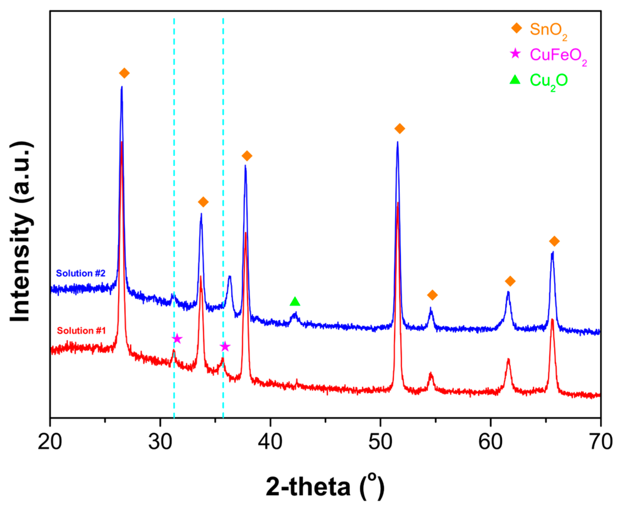
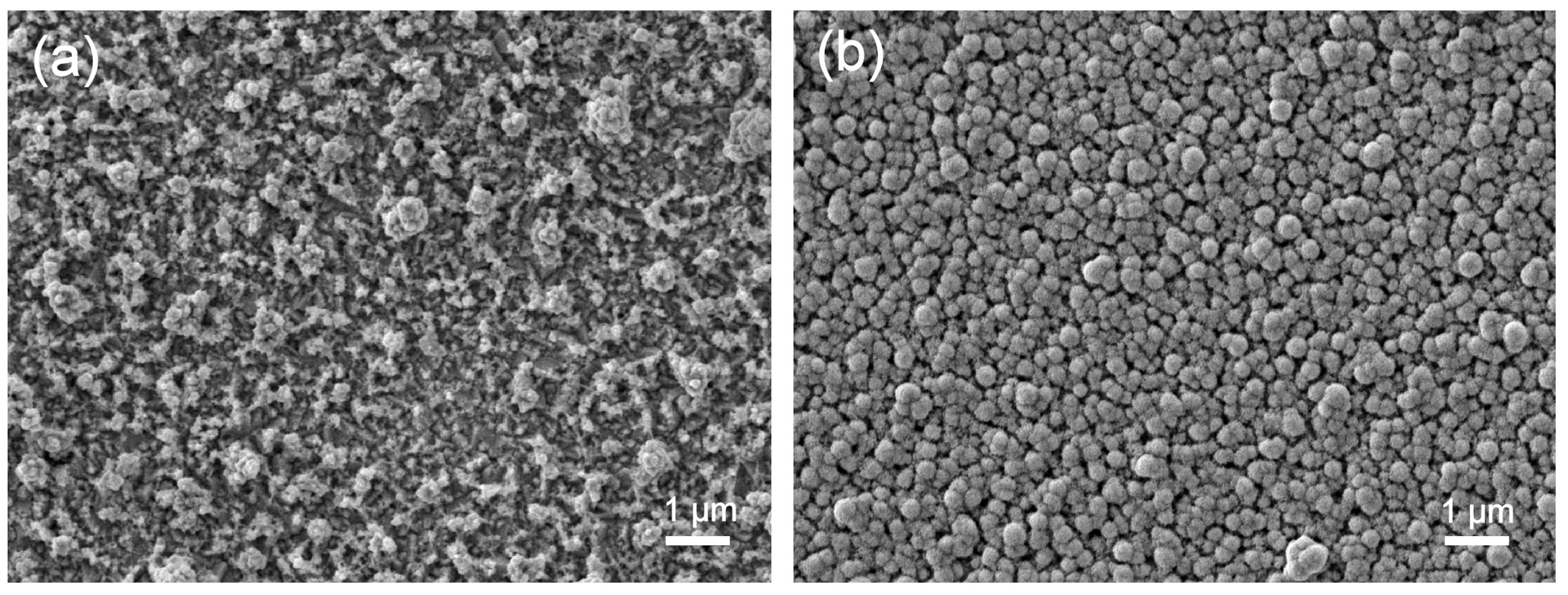
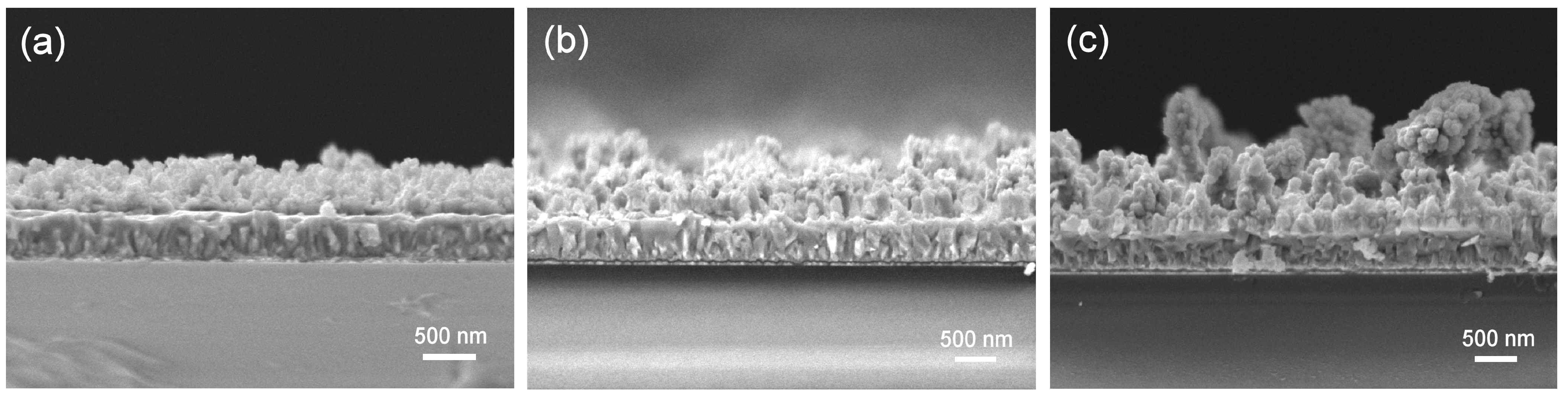
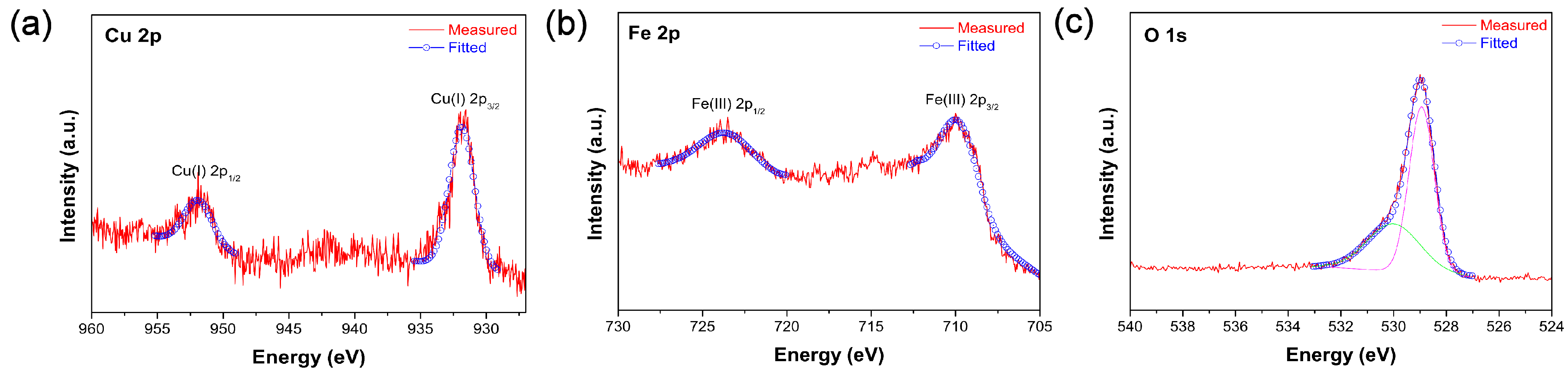
3. Results and Discussion

Non-aqueous based electrodeposition does not form metal hydroxide during the electrodeposition process, contrary to aqueous based electrodeposition. Thus, it influences the property of electrodeposited thin film. To examine this influence, the CuFeO2 film was electrodeposited using DMSO or distilled water solution with 1 mM Cu(NO3)2∙xH2O, 3 mM Fe(ClO4)3∙xH2O and 100 mM potassium perchlorate. Figure 1 shows the XRD patterns of the electrodeposited film in the electrolyte based DMSO and water solvents by applying a current density of −0.2 mA cm−2 for 60 min with post-annealing treatment at 650 °C for 1 h under N2 gas flow. All samples have diffraction peaks related to SnO2 (JCPDS No. 46-1088) from the FTO glass substrate. The diffraction peaks at 2θ = 31.26° and 35.8°, attributed to (006) and (012) orientations of the crystalline CuFeO2 (JCPDS No. 0175-2146) [39,40,41], were observed in the electrodeposited film in the DMSO solution. No other diffraction peaks, including those of metallic Cu or Fe, were observed. This means that electrodeposition using a DMSO solvent and post-annealing process produces a well-crystalline CuFeO2 film without any impurities. On the other hand, diffraction peaks at 2θ = 36.4° and 42.3°, corresponding to (111) and (200) orientations of the crystalline Cu2O (JCPDS No. 05-0667) [42,43], respectively, were observed in the electrodeposited film in the water solution. This indicates that the electrodeposited film in the water solution is the Cu2O film and not the CuFeO2 film.
The reason for this difference can be found in the mechanism of electrodeposition in different solvents. In general, the electrodeposited CuFeO2 film was formed by co-deposition of Cu2O and Fe2O3 via the following reactions [36]:
Fe3+(sol) + e → Fe2+(sol)
Cu2+(sol) + e → Cu+(sol)
2 Fe2+(sol) + 3/2 O2(sol) + 4 e → Fe2O3(s)
2 Cu+(sol) + 1/2 O2(sol) + 2 e → Cu2O(s)
Cu2O(s) + Fe2O3(s) → 2 CuFeO2(s)
In these reactions, the formation of Cu2O is more favored than that of Fe2O3 because the former is kinetically preferred to the latter [36]. Hence, the Cu2O film was formed in the electrodeposition using the water solution. Meanwhile, molecules of DMSO ((CH3)2SO) form strong complexes with copper (II) ions in the copper (II) nitrate hydrate [44]. This stabilizes the Cu ions in the electrodeposition bath, accelerating the Fe deposition in the film. Therefore, the CuFeO2 film was formed in the electrodeposition using DMSO solution.
The pristine electrodeposited CuFeO2 film from the DMSO solution was amorphous because no diffraction peaks were detected, except those related to the SnO2 from the FTO substrate (Figure S1). This means that the post-annealing treatment at 650 °C under N2 gas flow is necessary to transform the amorphous CuFeO2 into the crystalline one. In addition, it is clearly shown that the crystalline CuFeO2 film was homogeneously distributed, by element mapping of Cu, Fe and O from the top-view EDX characterization (Figure S2). Moreover, from the EDX characterization, it was demonstrated that the atomic ratio of Cu:Fe is almost 1:1 (9.87:8.88), which also indicates that the electrodeposited CuFeO2 film is stoichiometric. This suggests that the homogeneous and stoichiometric crystalline CuFeO2 film is successfully fabricated by the electrodeposition using a DMSO-based solution and post-annealing process under inert gas flow.
A complexing agent in the deposition electrolyte has been introduced to activate the Fe deposition for the electrodeposited CuFeO2 film. Therefore, it could have affected the characteristic of electrodeposited CuFeO2 film. Potassium perchlorate has been used to provide the chloride anion as a complexing agent in the electrodeposition of CuFeO2 film [9,36,37]. To investigate the effect of the complexing agent on the characteristics of electrodeposited CuFeO2 film, the electrodeposition was carried out using electrolyte with different potassium perchlorate concentrations. Figure 2 exhibits the XRD patterns of electrodeposited CuFeO2 film by applying a current density of −0.2 mA cm−2 for 60 min in the DMSO based electrolyte containing 1 mM Cu(NO3)2∙xH2O/3 mM Fe(ClO4)3∙xH2O/100 mM potassium perchlorate (Solution #1) and 4 mM Cu(NO3)2∙xH2O/12 mM Fe(ClO4)3∙xH2O/50 mM potassium perchlorate (Solution #2) after the post-annealing treatment at 650 °C under N2 gas flow. The diffraction peaks at 2θ = 31.26° and 35.8° are well matched with (006) and (012) orientations of the crystalline CuFeO2 in the electrodeposited film in Solution #1. On the other hand, in the electrodeposited film in Solution #2, the diffraction peak corresponding to the (006) orientation of CuFeO2 was also observed. However, the diffraction peak related to the (012) orientation of CuFeO2 was slightly shifted to the large angle (35.8° → 36.26°). It is assumed that the characteristic of CuFeO2 film was affected by the lattice parameter change or defect density [45]. In addition, the diffraction peak (2θ = 42.3°) attributed to the (111) orientation of the crystalline Cu2O was observed. This indicates that Cu2O was formed as the impurity when the film was electrodeposited in Solution #2.
Besides this, the morphologies of two films were totally different. As shown in Figure 3, irregularly shaped particles were covered in the electrodeposited film in Solution #1 (Figure 3a), while spherically shaped particles were deposited in the electrodeposited film in Solution #2 (Figure 3b). The average particle size was approximately 220 nm and some particles were agglomerated in the electrodeposited film in Solution #1. Meanwhile, the average particle size was approximately 315 nm and no particle aggregations were observed in the electrodeposited film in Solution #2. Based on these observations, it was concluded that the electrolyte containing more potassium perchlorate is adequate for making the pure crystalline CuFeO2 film with small particles using the galvanostatic electrodeposition. It is also demonstrated that the concentration of Cu/Fe salts was not a dominant factor determining the characteristic of the electrodeposited CuFeO2 film in the electrolyte condition, with a fixed ratio of Cu:Fe = 1:3.
The applied current density was controlled during the electrodeposition in the DMSO based electrolyte containing 1 mM Cu(NO3)2∙xH2O/3 mM Fe(ClO4)3∙xH2O/100 mM potassium perchlorate to study the property of the electrodeposited CuFeO2 film according to the current density in the galvanostatic mode. Figure 4a show the XRD patterns of the electrodeposited CuFeO2 film for 30 min by applying different current densities after post-annealing treatment at 650 °C under N2 gas flow. As illustrated in Figure 4a, all films have diffraction peaks at 2θ = 31.26° and 35.8°, attributed to the (006) and (012) orientations of the crystalline CuFeO2. Although they are weaker than those in the CuFeO2 electrodeposited for 60 min, due to the short deposition time, it clearly supports that the deposited film was the crystalline CuFeO2 without any impurities. In other words, the current density of galvanostatic electrodeposition did not have any influence on the composition of the electrodeposited film. However, it affected the morphology of the electrodeposited CuFeO2 film, as shown in Figure 4b–d. The irregular shaped CuFeO2 particles were formed on the substrate, similar to that in Figure 3a, while the aggregation of CuFeO2 particles became large when the applied current density was increased. This was likely to be due to the distinction of deposition speed, depending on the current density. The Cu/Fe ions in the solution were quickly moved to the substrate’s surface or pre-deposited CuFeO2 film by the strong electric field when the large current density was applied. Hence, the aggregation became severe around the previously deposited CuFeO2 particles in the electrodeposited film with the large current density.
Deposition time is a main factor in controlling the thickness of an electrodeposited film. Figure 5 shows the cross-section SEM images of electrodeposited CuFeO2 film with an applied current density of −0.1 mA cm−2 in the DMSO based electrolyte containing 1 mM Cu(NO3)2∙xH2O/3 mM Fe(ClO4)3∙xH2O/100 mM potassium perchlorate after post-annealing treatment at 650 °C under N2 gas flow. The electrodeposition for 20 min produced a homogeneous nanostructured CuFeO2 film with an average thickness of 500 nm, as shown in Figure 5a. The average thickness was increased to 875 nm after the electrodeposition for 40 min, as illustrated in Figure 5b. Finally, the nanostructured CuFeO2 film with an average thickness of 1000 nm was electrodeposited for 60 min (Figure 5c). Interestingly, the surface of nanostructured CuFeO2 film became rougher as the deposition time increased. In addition, the deposition of CuFeO2 film became slow as the deposition time passed. In other words, it means that the deposition ratio over time was not linear. The rougher nanostructured CuFeO2 film with the long deposition time was mainly due to the aggregation of CuFeO2 particles, while the non-linear deposition ratio over time was likely to be due to the relatively low conductivity of the electrode by the pre-deposited CuFeO2 film on the substrate.
In this way, it was demonstrated that electrodeposition in the DMSO based electrolyte containing more potassium perchlorate concentration with an applied current density of −0.1 mA cm−2 for deposition time below 30 min, and the post-annealing process at 650 °C under inert gas flow, produces nanostructured CuFeO2 film with less aggregations. The XPS analysis also confirms the composition of this film in detail. Figure 6 shows the XPS spectra of the electrodeposited CuFeO2 film in the DMSO based electrolyte containing 1 mM Cu(NO3)2∙xH2O/3 mM Fe(ClO4)3∙xH2O/100 mM potassium perchlorate with an applied current density of −0.1 mA cm−2 for 30 min after post-annealing treatment at 650 °C under N2 gas flow: Cu 2p (Figure 6a), Fe 2p (Figure 6b), and O 1s (Figure 6c). In Figure 6a, peaks located at 932 eV and 952 eV correspond to the binding energies of Cu (I) 2p3/2 and Cu (I) 2p1/2, respectively. This confirms the monovalent state of Cu (Cu+) in the CuFeO2 film [46,47]. In Figure 6b, peaks located at 710 eV and 723 eV are derived from the binding energies of Fe (III) 2p3/2 and Fe (III) 2p1/2, indicating the trivalent state of Fe (Fe3+) in the CuFeO2 film [46,47]. As shown in Figure 6c, the O 1s spectrum was deconvoluted into two peaks located at 529 eV and 530 eV, corresponding to the lattice oxygen species [48,49]. This is in good agreement with the typical chemical status of the crystalline CuFeO2 in the literature [36]. Based on these compositional and morphological analyses, it was concluded that the DMSO based solution with more complexing agent concentrations is a suitable electrolyte for the electrodeposition bath to fabricate the nanostructured CuFeO2 film without any impurities. In addition, it was demonstrated that it is possible to control the morphology of nanostructured CuFeO2 film without any compositional transitions by changing the current density and deposition time of galvanostatic electrodeposition.

4. Conclusions

In this study, the effect of deposition parameters, including the type of solvent, the condition of electrolyte, the applied current density and deposition time. on morphological and compositional characteristics of electrodeposited CuFeO2 film was investigated. As a result, in terms of the solvent, nanostructured CuFeO2 film was fabricated using the DMSO solution, while Cu2O film was formed using the water solution. Furthermore, the concentration of potassium perchlorate as a complexing agent in the electrolyte caused morphological change in the electrodeposited CuFeO2 film, as well as the compositional transition. On the other hand, the applied current density and deposition time did not have an influence on the composition of the electrodeposited CuFeO2 film. However, they caused the morphological changes in the electrodeposited CuFeO2 film. Along with previous studies (Table S1), it is expected that this will provide guidelines for selecting suitable electrodeposition conditions to fabricate nanostructured CuFeO2 composite electrode for specific applications, such as solar energy conversion devices, temperature sensors, photocatalysts, magnetoelectric devices and transparent conductive substrates.

Supplementary Materials

The following supporting information can be downloaded at: https://www.mdpi.com/article/10.3390/coatings12121820/s1, Figure S1: The XRD pattern of pristine electrodeposited CuFeO2 film in the DMSO-based electrolyte containing 1 mM Cu(NO3)2∙xH2O, 3 mM Fe(ClO4)3∙xH2O, and 100 mM potassium perchlorate by applying a current density of −0.2 mA cm−2 for 60 min; Figure S2: The top-view EDX characterization of the electrodeposited CuFeO2 film in the DMSO-based electrolyte containing 1 mM Cu(NO3)2∙xH2O, 3 mM Fe(ClO4)3∙xH2O, and 100 mM potassium perchlorate by applying a current density of −0.2 mA cm−2 for 60 min after post annealing treatment at 650 °C for 60 min under N2 gas flow; Table S1: Comparison of electrodeposition conditions and characteristics of electrodeposited film between previous studies and this work.

Funding

This research was supported in part by the National Research Foundation of Korea (NRF), grant funded by the Korean government (MSIT) (NRF-2021R1F1A1059126) and in part by the program of Future Hydrogen Original Technology Development (NRF-2021M3I3A1084649) through the National Research Foundation of Korea (NRF), funded by the Korean government (MSIT).

Institutional Review Board Statement

Not applicable.

Informed Consent Statement

Not applicable.

Data Availability Statement

The data presented in this study are available on request from the corresponding author.

Conflicts of Interest

The authors declare no conflict of interest.

References

  1. Chen, H.-Y.; Wu, J.-H. Transparent conductive CuFeO2 thin films prepared by sol-gel processing. Appl. Surf. Sci. 2012, 258, 4844–4847. [Google Scholar] [CrossRef]
  2. Deng, Z.; Fang, X.; Wang, X.; Wu, S.; Dong, W.; Shao, J.; Tao, R. Characterization of amorphous p-type transparent CuFeO2 thin films prepared by radio frequency magnetron sputtering method at room temperature. Thin Solid Film. 2015, 589, 17–21. [Google Scholar] [CrossRef]
  3. Mohamed, H.; Chikoidze, E.; Ratep, A.; Elsoud, A.M.A.; Boshta, M.; Osman, M.B.S. Synthesis of conducting single-phase CuFeO2 thin films by spray pyrolysis technique. Mater. Sci. Semicond. Process 2020, 107, 104831. [Google Scholar] [CrossRef]
  4. Elgazzar, E.; Tataroglu, A.; Al-Ghamdi, A.A.; Al-Tuki, Y.; Farooq, W.A.; El-Tantawy, F.; Yakuphanoglu, F. Thermal sensors based on delafossite film/p-silicon diode for low-temperature measurements. Appl. Phys. A 2016, 122, 617. [Google Scholar] [CrossRef]
  5. Sinnarasa, I.; Thimont, Y.; Barnabe, A.; Beaudhuin, M.; Moll, A.; Schorne-Pinto, J.; Tailhades, P.; Presmanes, L. Microstructural and transport properties of Mg-doped CuFeO2 thin films: A promising material for high accuracy miniaturized temperature sensors based on the Seebeck effect. J. Alloys Compd. 2020, 827, 154199. [Google Scholar] [CrossRef]
  6. Xia, N.; Shi, L.; Xia, Z.; Chen, B.; Jin, Z.; Wang, Y.; Ouyang, Z.; Zuo, H.; Shen, Y. Dynamic behavior of magnetoelectric coupling of CuFeO2 induced by a high magnetic field. J. Appl. Phys. 2014, 115, 114107. [Google Scholar] [CrossRef]
  7. Dai, H.; Ye, F.; Li, T.; Chen, Z.; Cao, X.; Wang, B. Impact of Li doping on the microstructure, defects, and physical properties of CuFeO2 multiferroic ceramics. Ceram. Int. 2019, 45, 24570–24577. [Google Scholar] [CrossRef]
  8. Crespo, C.T. Potentiality of CuFeO2-delafossite as a solar energy converter. Sol. Energy 2018, 163, 162–166. [Google Scholar] [CrossRef]
  9. Read, C.G.; Park, Y.; Choi, K.-S. Electrochemical synthesis of p-type CuFeO2 electrodes for use in a photoelectrochemical cell. J. Phys. Chem. Lett. 2012, 3, 1872–1876. [Google Scholar] [CrossRef]
  10. Zhu, T.; Deng, Z.; Fang, X.; Huo, Z.; Wang, S.; Dong, W.; Shao, J.; Tao, R.; Song, C.; Wang, L. High photovoltages of CuFeO2 based p-type dye-sensitized solar cells. J. Alloys Compd. 2016, 685, 836–840. [Google Scholar] [CrossRef]
  11. Jin, Y.; Chumanov, G. Solution synthesis of pure 2H CuFeO2 at low temperature. RSC Adv. 2016, 6, 26392–26397. [Google Scholar] [CrossRef]
  12. Prevot, M.S.; Guijarro, N.; Sivula, K. Enhancing the performance of a robust sol-gel processed-type delafossite CuFeO2 photocathode for solar water reduction. ChemSusChem 2015, 8, 1359–1367. [Google Scholar] [CrossRef]
  13. Jang, Y.J.; Park, Y.B.; Kim, H.E.; Choi, Y.H.; Choi, S.H.; Lee, J.S. Oxygen-intercalated CuFeO2 photocathode fabricated by hybrid microwave annealing for efficient solar hydrogen production. Chem. Mater. 2016, 28, 6054–6061. [Google Scholar] [CrossRef]
  14. Oh, Y.; Yang, W.; Kim, J.; Jeong, S.; Moon, J. Enhanced photocurrent of transparent CuFeO2 photocathodes by self-light-harvesting architecture. ACS Appl. Mater. Interfaces 2017, 9, 14078–14087. [Google Scholar] [CrossRef]
  15. Boudoire, F.; Liu, Y.; Formal, F.L.; Guijarro, N.; Lhermitte, C.R.; Sivula, K. Spray synthesis of CuFeO2 photocathodes and in-operando assessment of charge carrier recombination. J. Phys. Chem. C 2021, 125, 10883–10890. [Google Scholar] [CrossRef]
  16. Prevot, M.S.; Jeanbourquin, X.A.; Bouree, W.S.; Abdi, F.; Friedrich, D.; Krol, R.; Guijarro, N.; Formal, F.L.; Sivula, K. Evaluating charge carrier transport and surface states in CuFeO2 photocathodes. Chem. Mater. 2017, 29, 4952–4962. [Google Scholar] [CrossRef]
  17. Liu, Q.-L.; Zhao, Z.-Y.; Zhao, R.-D.; Yi, J.-H. Fundamental properties of delafossite CuFeO2 as photocatalyst for solar energy conversion. J. Alloys Compd. 2020, 819, 153032. [Google Scholar] [CrossRef]
  18. Preethi, S.; Vivek, S.; Priya, R.; Balakumar, S.; Babu, K.S. Enhanced photocatalytic performance of CuFeO2-ZnO heterostructures for methylene blue degradation under sunlight. J. Mater. Sci. Mater. Electron. 2021, 32, 22256–22269. [Google Scholar] [CrossRef]
  19. Tu, L.-W.; Chang, K.-S. Hydrothermal fabrication and photocatalytic study of delafossite (CuFeO2) thin films on fluorine-doped tin oxide substrate. Mater. Chem. Phys. 2021, 267, 124620. [Google Scholar] [CrossRef]
  20. Barnabe, A.; Mugnier, E.; Presmanes, L.; Thailhades, P. Preparation of delafossite CuFeO2 thin films by rf-sputtering on conventional glass substrate. Mater. Lett. 2006, 60, 3468–3470. [Google Scholar] [CrossRef]
  21. Zhu, T.; Deng, Z.; Fang, X.; Dong, W.; Shao, J.; Tao, R.; Wang, S. Room temperature deposition of amorphous p-type CuFeO2 and fabrication of CuFeO2/n-Si heterojunction by RF sputtering method. Bull. Mater. Sci. 2016, 39, 883–887. [Google Scholar] [CrossRef] [Green Version]
  22. Ziani, N.; Aubry, E.; Martin, N.; Hirsinger, L.; Billard, A.; Briois, P.; Belkaid, M.S.; Yazdi, M.A.P. Influence of substrate temperature on delafossite CuFeO2 films synthesized by reactive magnetron sputtering. J. Alloys Compd. 2021, 876, 160169. [Google Scholar] [CrossRef]
  23. Li, S.Z.; Liu, J.; Wang, X.Z.; Yan, B.W.; Li, H.; Liu, J.-M. Epitaxial growth of delafossite CuFeO2 thin films by pulse laser deposition. Phys. B Condens. Mater. 2012, 407, 2412–2415. [Google Scholar] [CrossRef]
  24. Joshi, T.; Senty, T.R.; Trappen, R.; Zhou, J.; Chen, S.; Ferrari, P.; Borisov, P.; Song, X.; Holcomb, M.B.; Bristow, A.D.; et al. Structural and magnetic properties of epitaxial delafossite CuFeO2 thin films grown by pulsed laser deposition. J. Appl. Phys. 2015, 117, 013908. [Google Scholar] [CrossRef]
  25. Luo, S.; Fluri, A.; Zhang, S.; Liu, X.; Döbeli, M.; Harrington, G.F.; Tu, R.; Pergolesi, D.; Ishihara, T.; Lippert, T. Thickness-dependent microstructural properties of heteroepitaxial (00.1) CuFeO2 thin films on (00.1) sapphire by pulsed laser deposition. J. Appl. Phys. 2020, 127, 065301. [Google Scholar] [CrossRef]
  26. Zhang, L.; Li, P.; Huang, K.; Tang, Z.; Liu, G.; Li, Y. Chemical solution deposition and transport properties of epitaxial CuFeO2 thin films. Mater. Lett. 2011, 65, 3289–3291. [Google Scholar] [CrossRef]
  27. Gupta, R.K.; Cavas, M.; Al-Ghamdi, A.A.; Gafer, Z.H.; El-Tantawy, F.; Yakuphanoglu, F. Electrical and photoresponse properties of Al/p-CuFeO2/p-Si/Al MTCOS photodiode. Sol. Energy 2013, 92, 1–6. [Google Scholar] [CrossRef]
  28. Ito, M.; Izawa, C.; Watanabe, T. Direct fabrication of a CuFeO2/Fe photocathode for solar hydrogen production by hydrothermal method. Chem. Lett. 2017, 46, 814–816. [Google Scholar] [CrossRef]
  29. Yuan, J.; Yang, L.; Hao, C. Lithium-doped CuFeO2 thin film electrodes for photoelectrochemical reduction of carbon dioxide to methanol. J. Electrochem. Soc. 2019, 166, H718. [Google Scholar] [CrossRef]
  30. Aqaei, F.; Zare, M.; Shafiekhani, A. Role of plasmonic Au nanoparticles embedded in the diamond-like carbon overlayer in the performance of CuFeO2 solar photocathodes. J. Solid State Electrochem. 2021, 25, 1139–1150. [Google Scholar] [CrossRef]
  31. Yin, G.; Liu, C.; Shi, T.; Ji, D.; Yao, Y.; Chen, Z. Porous BiVO4 coupled with CuFeO2 and NiFe layered double hydroxide as highly-efficient photoanode toward boosted photoelectrochemical water oxidation. J. Photochem. Photobiol. A Chem. 2022, 426, 113742. [Google Scholar] [CrossRef]
  32. Alkhayatt, A.H.O.; Thahab, S.M.; Zgair, I.A. Structure, surface morphology and optical properties of post-annealed delafossite CuFeO2 thin films. Optik 2016, 127, 3745–3749. [Google Scholar] [CrossRef]
  33. Garcia-Torregrosa, I.; Geertzema, Y.G.; Ismail, A.S.M.; Lee, T.-L.; de Grioot, F.M.F.; Weckhyusen, B.M. Facile two-step synthesis of delafossite CuFeO2 photocathodes by ultrasonic spray pyrolysis and hybrid microwave annealing. ChemPhotoChem 2019, 3, 1238–1245. [Google Scholar] [CrossRef]
  34. Dharmadasa, I.M.; Haigh, J. Strengths and advantages of electrodeposition as a semiconductor growth technique for applications in microelectronic devices. J. Electrochem. Soc. 2006, 153, G47–G52. [Google Scholar] [CrossRef]
  35. Xiao, F.; Hangarter, C.; Yoo, B.; Rheem, Y.; Lee, K.-H.; Myung, N.V. Recent progress in electrodeposition of thermoelectric thin films and nanostructures. Electrochim. Acta 2008, 53, 8103–8117. [Google Scholar] [CrossRef]
  36. Riveros, G.; Garin, C.; Ramirez, D.; Dalchiele, E.A.; Marotti, R.E.; Pereyra, C.J.; Spera, E.; Gomez, H.; Grez, P.; Martin, F.; et al. Delafossite CuFeO2 thin films electrochemically grown from a DMSO based solution. Electrochim. Acta 2015, 164, 297–306. [Google Scholar] [CrossRef]
  37. Kang, U.; Park, H. A facile synthesis of CuFeO2 and CuO composite photocatalyst films for the production of liquid formate from CO2 and water over a month. J. Mater. Chem. A 2017, 5, 2123–2131. [Google Scholar] [CrossRef]
  38. Yan, Z.; Liu, H.; Hao, Z.; Yu, M.; Chen, X.; Chen, J. Electrodeposition of (hydro)oxides for an oxygen evolution electrode. Chem. Sci. 2020, 11, 10614–10625. [Google Scholar] [CrossRef] [PubMed] [Green Version]
  39. Oh, Y.; Yang, W.; Tan, J.; Lee, H.; Park, J.; Moon, J. Photoelectrodes based on 2D opals assembled from Cu-delafossite double-shelled microspheres for an enhanced photoelectrochemical response. Nanoscale 2018, 10, 3720–3729. [Google Scholar] [CrossRef]
  40. Oh, Y.; Yang, W.; Tan, J.; Lee, H.; Park, J.; Moon, J. Boosting visible light harvesting in p-type ternary oxides for solar-to-hydrogen conversion using inverse opal structure. Adv. Funct. Mater. 2019, 29, 1900194. [Google Scholar] [CrossRef]
  41. Wang, M.; Liu, C.; Shi, H.; Long, T.; Zhang, C.; Liu, B. Facile synthesis of chitosan-derived maillard reaction productions coated CuFeO2 with abundant oxygen vacancies for higher Fenton-like catalytic performance. Chemosphere 2021, 283, 131191. [Google Scholar] [CrossRef]
  42. Choudhary, S.; Sarma, J.V.N.; Pande, S.; Girad, S.A.; Turban, P.; Lepine, B.; Gangopadhyay, S. Oxidation mechanism of thin Cu films: A gateway towards the formation of single oxide phase. AIP Adv. 2018, 8, 055114. [Google Scholar] [CrossRef] [Green Version]
  43. Luo, J.; Steier, L.; Son, M.-K.; Schreier, M.; Mayer, M.T.; Grätzel, M. Cu2O nanowire photocathodes for efficient and durable solar water splitting. Nano Lett. 2016, 16, 1848–1857. [Google Scholar] [CrossRef] [PubMed]
  44. Mamyrbekova, A.K.; Mamitova, A.D.; Turebekova, G.; Gul, K.; Mamyrbekova, A.K. Kinetics and mechanism of cathodic processes at electrolysis of Cu(NO3)2∙3H2O solution in dimethyl sulfoxide. Asian J. Chem. 2016, 28, 525–528. [Google Scholar] [CrossRef]
  45. De, M.; Gupta, S.P.S. Lattice imperfection studies in polycrystalline materials by x-ray diffraction line-profile analysis. Pramana 1984, 23, 721–744. [Google Scholar] [CrossRef]
  46. Chen, H.-Y.; Fu, J.-R. Delafossite-CuFeO2 thin films prepared by atmospheric pressure plasma annealing. Mater. Lett. 2014, 120, 47–49. [Google Scholar] [CrossRef]
  47. Xiong, D.; Qi, Y.; Li, X.; Tao, H.; Chen, W.; Zhao, X. Hydrothermal synthesis of delafossite CuFeO2 crystals at 100 °C. RSC Adv. 2015, 5, 49280–49286. [Google Scholar] [CrossRef]
  48. Li, Z.; Wu, W.; Wang, M.; Wang, Y.; Ma, X.; Luo, L.; Chen, Y.; Kan, K.; Pan, Y.; Li, H.; et al. Ambient-pressure hydrogenation of CO2 into long-chain olefins. Nat. Commun. 2022, 13, 2396. [Google Scholar] [CrossRef] [PubMed]
  49. Son, M.-K.; Seo, H.; Watanabe, M.; Shiratani, M.; Ishihara, T. Characteristics of crystalline sputtered LaFeO3 thin films as photoelectrochemical water splitting photocathodes. Nanoscale 2020, 12, 9653–9660. [Google Scholar] [CrossRef] [PubMed]
Figure 1. XRD patterns of electrodeposited film in electrolyte-based DMSO (red) and water (black) solvents. Electrodeposition was carried out by applying a current density of −0.2 mA cm−2 for 60 min and the films were annealed at 650 °C for 1 h under N2 gas flow after electrodeposition.
Coatings 12 01820 g001
Figure 2. XRD patterns of electrodeposited CuFeO2 film by applying a current density of −0.2 mA cm−2 for 60 min in DMSO based electrolytes with different potassium perchlorate concentrations. Solution #1 (red) contained 1 mM Cu(NO3)2∙xH2O/3 mM Fe(ClO4)3∙xH2O/100 mM potassium perchlorate, while Solution #2 (blue) contained 4 mM Cu(NO3)2∙xH2O/12 mM Fe(ClO4)3∙xH2O/50 mM potassium perchlorate. Electrodeposited films were annealed at 650 °C for 1 h under N2 gas flow.
Coatings 12 01820 g002
Figure 3. Top-view SEM images of electrodeposited CuFeO2 films when applying a current density of −0.2 mA cm−2 for 60 min in DMSO based electrolytes with different potassium perchlorate concentrations: (a) Solution #1 containing 1 mM Cu(NO3)2∙xH2O/3 mM Fe(ClO4)3∙xH2O/100 mM potassium perchlorate and (b) Solution #2 containing 4 mM Cu(NO3)2∙xH2O/12 mM Fe(ClO4)3∙xH2O/50 mM potassium perchlorate. Electrodeposited films were annealed at 650 °C for 1 h under N2 gas flow.
Coatings 12 01820 g003
Figure 4. (a) XRD patterns of electrodeposited CuFeO2 film by applying different current densities: −0.1 mA cm−2 (black), −0.2 mA cm−2 (red), and −0.3 mA cm−2 (green). Top view SEM images of electrodeposited CuFeO2 film by applying different current densities of (b) −0.1 mA cm−2, (c) −0.2 mA cm−2, and (d) −0.3 mA cm−2. Electrodeposition was carried out in DMSO based electrolytes containing 1 mM Cu(NO3)2∙xH2O/3 mM Fe(ClO4)3∙xH2O/100 mM potassium perchlorate for 30 min. Electrodeposited films were annealed at 650 °C for 1 h under N2 gas flow.
Coatings 12 01820 g004
Figure 5. Cross-section SEM images of electrodeposited CuFeO2 film with an applied current density of −0.1 mA cm−2 in DMSO based electrolyte containing 1 mM Cu(NO3)2∙xH2O/3 mM Fe(ClO4)3∙xH2O/100 mM potassium perchlorate for different deposition time: (a) 20 min (b) 40 min and (c) 60 min. Samples were annealed at 650 °C for 1 h under N2 gas flow after electrodeposition.
Coatings 12 01820 g005
Figure 6. XPS spectra of electrodeposited CuFeO2 film in DMSO based electrolyte containing 1 mM Cu(NO3)2∙xH2O/3 mM Fe(ClO4)3∙xH2O/100 mM potassium perchlorate with an applied current density of −0.1 mA cm−2 for 30 min after post-annealing treatment at 650 °C for 1hr under N2 gas flow: (a) Cu 2p, (b) Fe 2p, and (c) O 1s.
Coatings 12 01820 g006
Table 1. General characteristics of delafossite-structured CuFeO2 [1,2,3,8,9,16].
CharacteristicsValues
Conductivity1.53~2 S cm−1
Carrier mobility0.2 cm2 V−1 s−1
Hall coefficient1.84 × 106 m2 C−1
Band gap1.1~1.6 eV
Absorption coefficientUp to 107 m−1
Publisher’s Note: MDPI stays neutral with regard to jurisdictional claims in published maps and institutional affiliations.

