Article

Laser Protection Properties of Multi-Band Non-Regularized Highly Reflective Films

1
School of Optoelectronic Engineering, Xi’an Technological University, Xi’an 710021, China
2
Aircraft and Propulsion Laboratory, Ningbo Institute of Technology, Beihang University, Ningbo 315800, China
*
Author to whom correspondence should be addressed.
Coatings 2022, 12(11), 1614; https://doi.org/10.3390/coatings12111614
Submission received: 27 September 2022 / Revised: 19 October 2022 / Accepted: 21 October 2022 / Published: 23 October 2022
(This article belongs to the Special Issue Optical Thin Films: Preparation, Application and Development)

Abstract

:
With the increasing exploitation of lasers, single-band laser protection has been extensively studied. However, single-band laser protection techniques have remained expensive and failed to meet protection requirements for multi-band lasers. In addition, the actual use of protective films requires a specific transmittance, which is generally not met by regular films. Here, we deposited three non-regularized highly reflective films using SiO2 as the low-refractive-index material and TiO2, HfO2, and Ta2O5 as the high-refractive-index materials by thermal evaporation for achieving multi-band laser protection. To verify the effectiveness of the films, the variation in transmittance, damage threshold, standing-wave electric field, and damage morphology of the films were analyzed at two laser wavelengths, and their protection mechanisms were evaluated based on optical properties and damage resistance. The results showed that the reflectances of the prepared non-regularized films at 1064 nm and 532 nm were greater than 99%, and the laser-induced damage thresholds for TiO2/SiO2, HfO2/SiO2, and Ta2O5/SiO2 films were 5.99, 5.89, and 9.99 J/cm2 at 1064 nm and 3.04 J/cm2, 1.48 J/cm2, and 4.93 J/cm2 at 532 nm, respectively, demonstrating good laser protection. The present work provides a practical and effective solution for multi-band laser protection and the prepared films may be used in numerous laser applications.

1. Introduction

Although the widespread use of lasers has accelerated technological progress, it has also increased the adverse effects of lasers on equipment and human health. If not prevented in time, they often cause system failure or paralysis. To reduce the risks associated with laser use, laser protection lenses must be designed to protect against potentially harmful laser wavelengths. In addition, developing safety rules during laser use [1], preparation of laser protection glasses for specific wavelengths [2], developing optical limiting materials [3], and designing and preparing trap filters [4] were proposed. Therefore, laser protection technologies [5] must be developed to reduce industrial and medical costs while realizing widespread laser applications.
The mechanism of laser damage to the target mainly involves thermal action, which causes ablation damage caused by high energy. Therefore, laser protection research relies on laser reflection and high thermal barriers. After years of research on high thermal barriers, laser protection films and materials have been increasingly studied to implement them in practice [6,7]. For example, to meet the increasing demand for infrared transmission windows [8], a sapphire surface was coated with a double-layer film to improve its resistance to laser damage at high temperatures [9].
However, most studies were conducted for protection against a single waveband, such as the development of laser protective goggles, although many current scenarios require multi-band protection, such as laser-based beauty and cosmetic procedures, laser cutting, and laser measurement. The laser output involves multiple bands; thus, a single-band protective film falls short of providing sufficient protection or even causes serious accidents. Therefore, multi-band laser protection films require urgent investigation.
Currently, researchers have determined that multi-band laser protection can be further reduced to the study of two-band laser protection [10] and the prepared films resulted in average optical density values of 8.832 and 10.191 [11], respectively, for the target bands. Among the materials currently used for laser protection, oxides [12,13] are preferred owing to their high melting point, good stability, and relatively high laser-induced damage threshold [14]. HfO2 and SiO2 provide significant advantages in laser protection and achieve specific transmittance at multiple wavelengths due to their good optical properties [15,16,17]. Previous studies have narrowly focused on HfO2/SiO2 materials. In addition to HfO2 and SiO2, TiO2 is durable and offers ideal optical properties [18,19], and Ta2O5 has good thermal stability and was applied to transmission-enhancing films and filters [20]. Thus, in this work, SiO2 was used as the low-refractive-index material, and TiO2, HfO2, and Ta2O5 were used as the high-refractive-index materials for the design and development of multi-band laser protection films.
In addition, most applications require protective films to meet a specific transmittance to prevent adverse effects at certain laser wavelengths, a requirement often not met by gauge films. Thus, we developed non-regularized highly reflective films tailored for specific applications. Since the human eye is most sensitive to the green color near 550 nm, the closest laser wavelength to 550 nm is 532 nm, while 1064 nm lasers are widely used in industry and medicine. Therefore, to study multi-band laser protection, two bands, 1050–1080 nm and 520–540 nm, were selected based on the widely used 1064 nm and 532 nm lasers.
To meet the demand for laser protection applications, we designed and prepared dual-band, non-regularized, highly reflective TiO2/SiO2, HfO2/SiO2, and Ta2O5/SiO2 films by thermal evaporation. The damage resistance of the samples was determined by optical measurement methods using 1064 nm and 532 nm lasers to induce damage to the films to evaluate their high-energy laser protection properties, and the optical properties were measured using a spectrophotometer. In addition, the damage mechanism was analyzed using an optical microscope and white-light interferometer.

2. Experimental Procedure

The three non-regularized highly reflective films were deposited by thermal evaporation in a vacuum coater (Optorun, Japan, OTFC-900). Before preparation, the K9 glass substrate was wiped with a 3:1 alcohol:ether mixture and then placed in an iron ring to dry under ultraclean bench light. The deposition process is the same for all samples. After cleaning the vacuum chamber, evacuating, melting, coating, and degassing and so on, the samples are finally completed. During the plating process, the background vacuum was 9.0 × 10⁻⁴ Pa, the film-forming holding vacuum was 2.0 × 10⁻² Pa, and the evaporation rate was 3 A/s. Continuous heating was required for both deposition preparation and the deposition process, and a baking temperature of 200 °C was maintained. The thin film deposition process parameters are shown in Table 1.
The designed films were based on a coating stack of G|(HL)xH|A, which was optimized to obtain a conformal non-regularized film (G represents the substrate material K9 glass, and L and H represent low-refractive-index materials (SiO2) and high-refractive-index materials (TiO2, HfO2, and Ta2O5)) with a quarter-wavelength optical thickness. In Figure 1, the theoretical transmittance spectral curves of the three highly reflective films are shown.
The theoretical average reflectance in the design band in Figure 1a was greater than 97%, 97.02% at 1064 nm and 97.80% at 532 nm. The theoretical average reflectance in the design band in Figure 1b was greater than 99%, 99.62% at 1064 nm and 99.12% at 532 nm. The theoretical average reflectance in the design band in Figure 1c was greater than 98%, 98.69% at 1064 nm and 98.19% at 532 nm. The three samples ensured that the average reflectance of the same film in the two design wavelengths was comparable and that the difference in the reflectance of the same film at the two action wavelengths did not exceed 0.8%, meeting the design requirements.

3. Results and Discussion

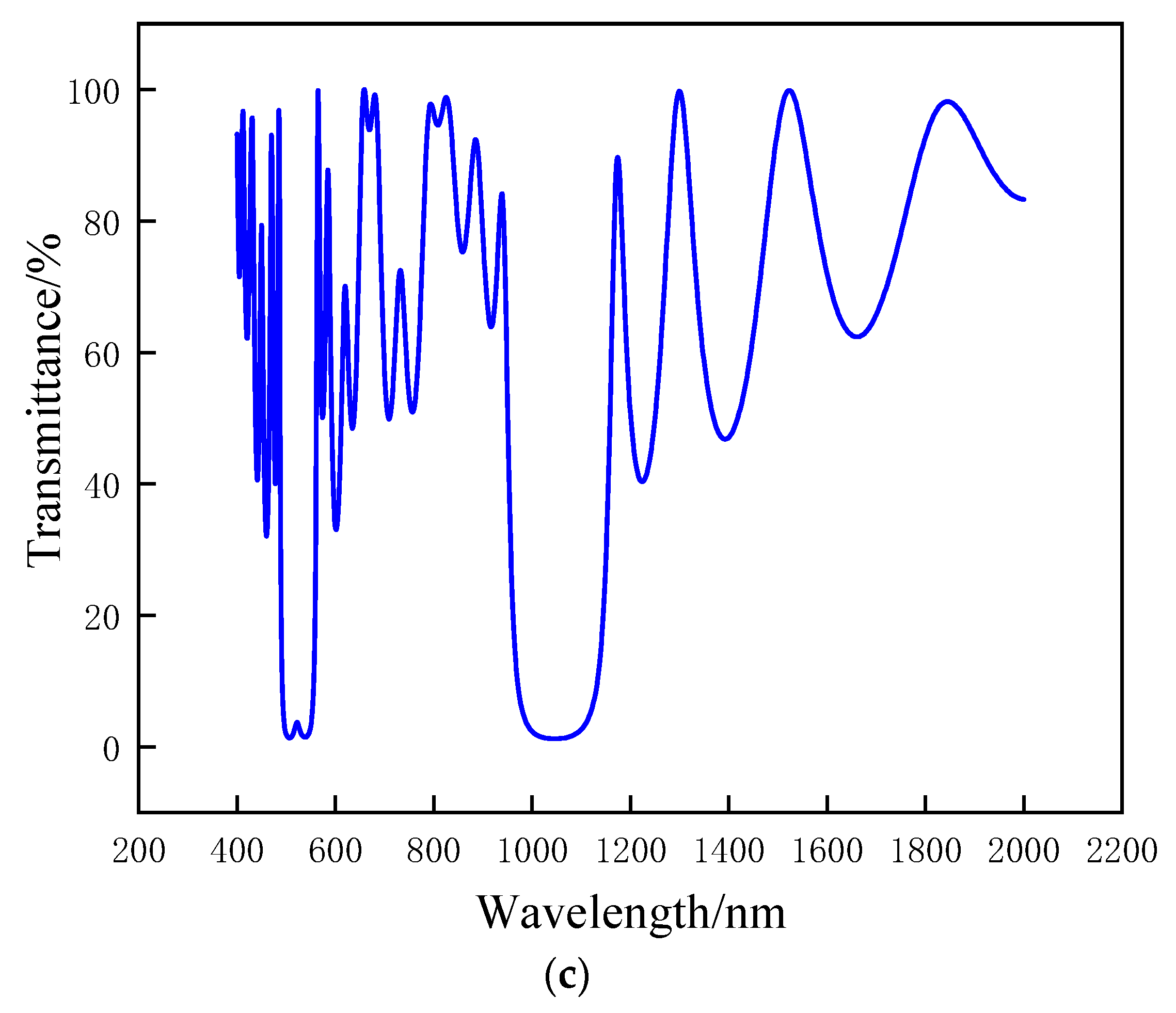
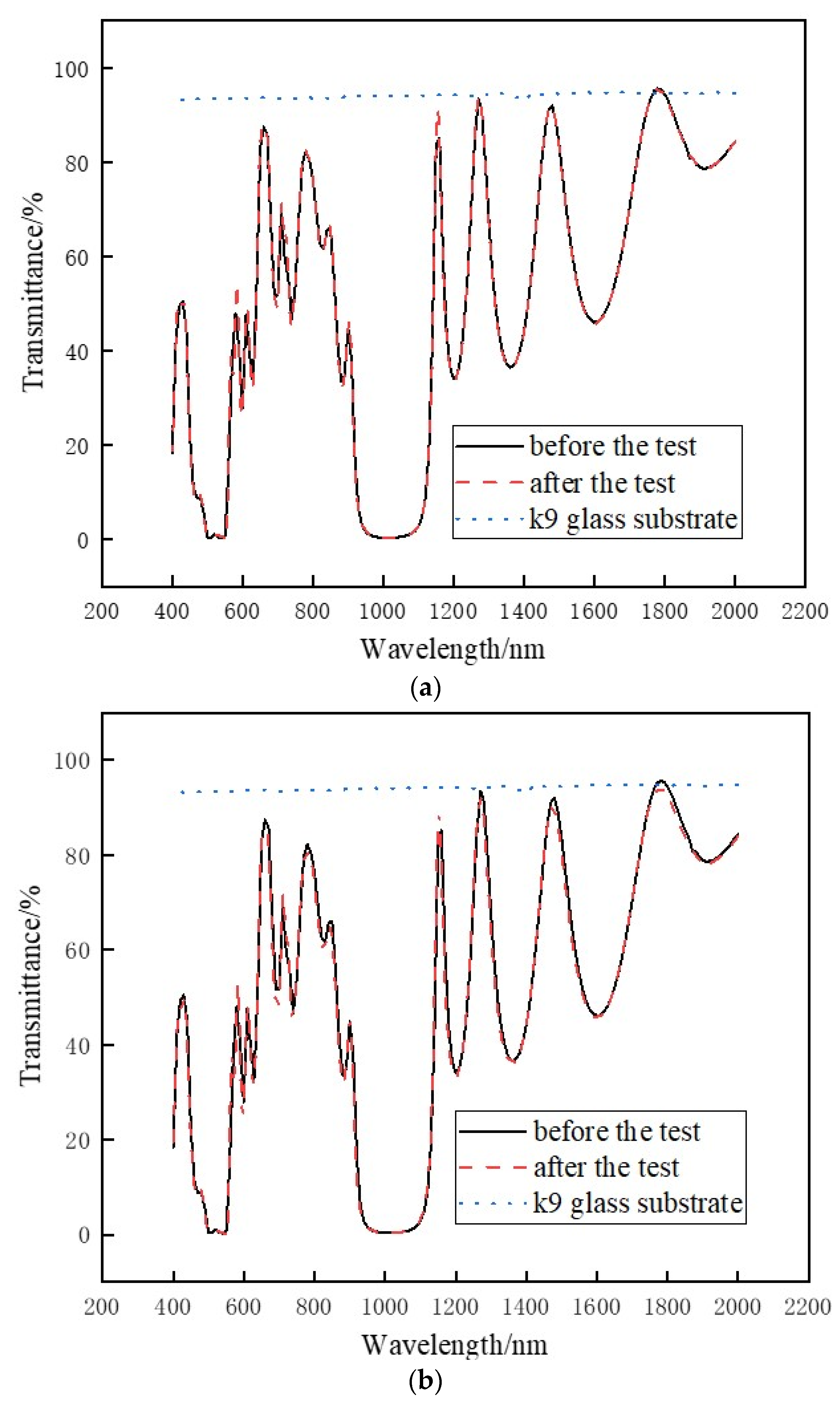
3.1. Optical Properties

To check whether the reflectance of the prepared films met the requirements of highly reflective laser protection applications, a Lambda 900 spectrophotometer was used to measure the transmittance values of the laser protection films before and after the protection test, and the transmittance spectra in the wavelength range of 400–2000 nm were obtained, as shown in Figure 2, Figure 3 and Figure 4.
The transmittance of pure K9 was about 91% in the visible and infrared regions. The transmittance was reduced when the designed material was deposited on the K9 substrate. In Figure 2, Figure 3 and Figure 4, the average reflectances of the samples tested in the design band were greater than 98% and the reflectances tested at 1064 nm and 532 nm were greater than 99%, which meets the design requirements. In addition, the spectra remained in good agreement in the target area. The comparison of post- and pre-test spectral curves showed that the transmittances of the three films decreased more substantially after the action of the 532 nm laser compared to the 1064 nm laser, indicating that the 532 nm laser influenced the film transmittance.

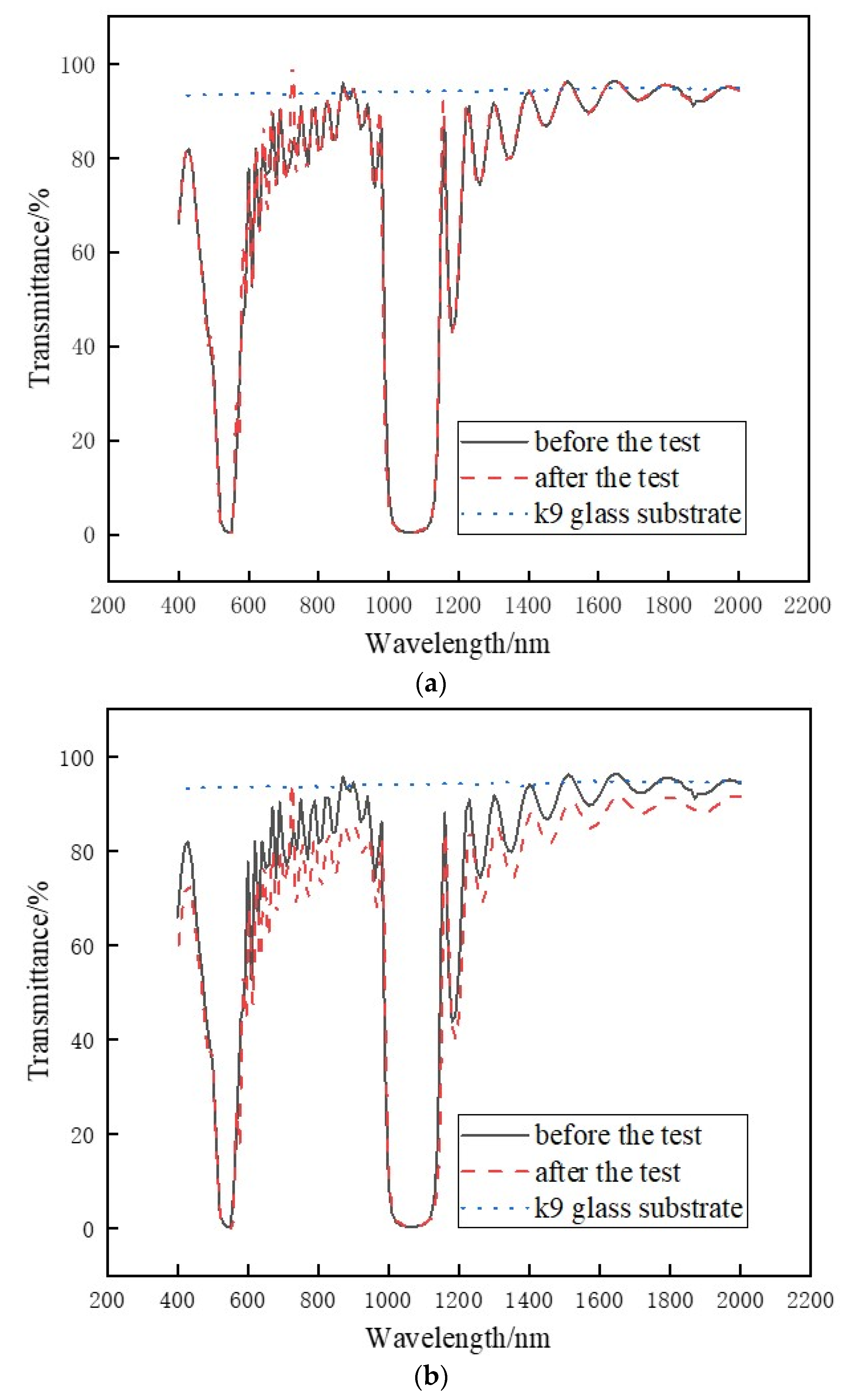
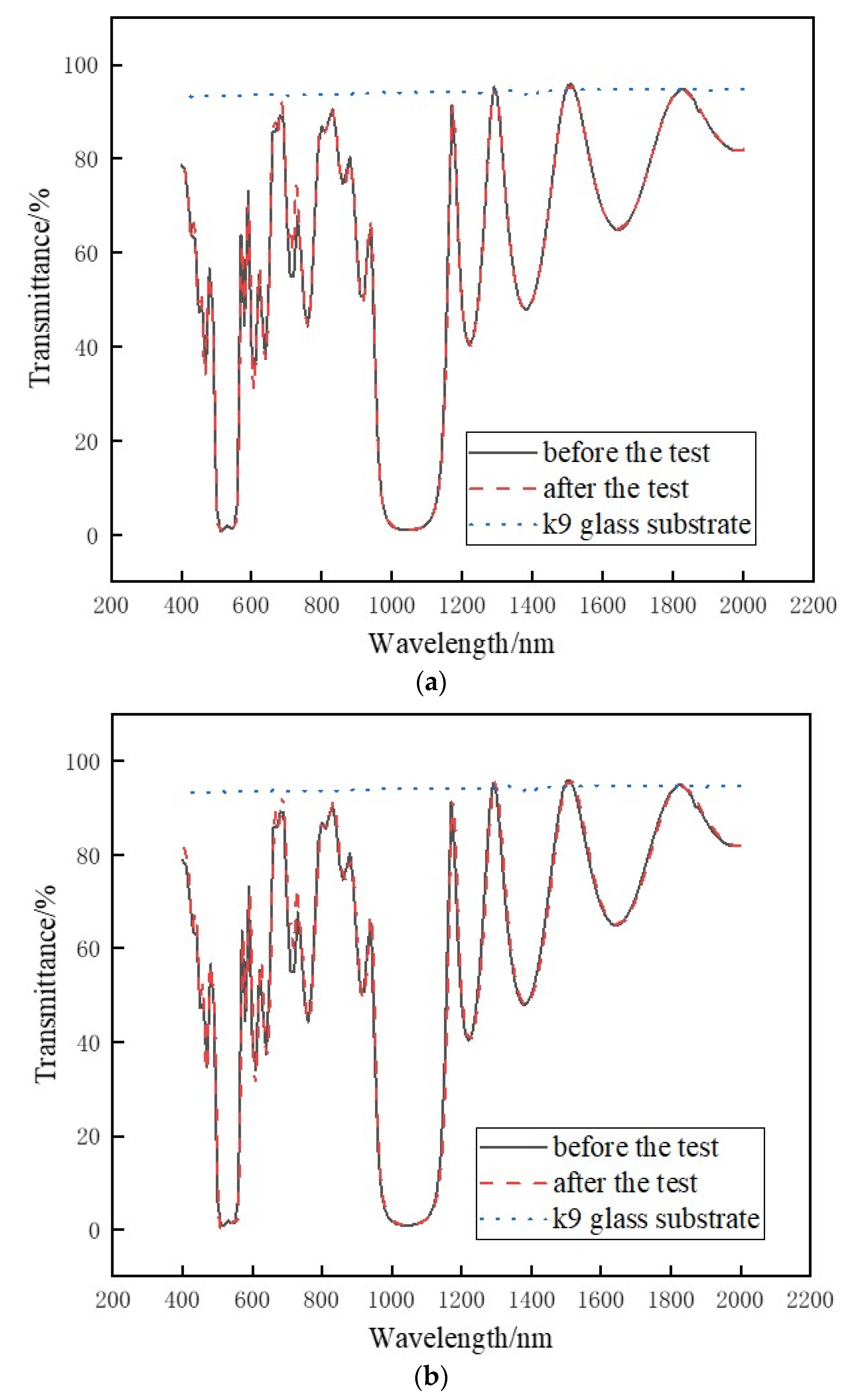
3.2. Laser Protection Properties

To determine the protective effects of the non-regularized laser protection films in the designed waveband and ensure the consistency of laser protection performance testing (reduce test errors and improve the credibility and comparability of data), a dual-wavelength damage threshold tester was used, where two lasers shared the same optical path. The system was equipped with two common wavelengths (1064 nm and 532 nm) of Nd:YAG nanosecond pulsed lasers, both outputting Gaussian fundamental frequency signals with an operating frequency of 10 Hz, a pulse width of 10 ns, and a spot diameter of 0.8 mm. According to the international standard ISO 11254 [21] test requirements, a one-on-one test is taken and the laser protection characteristics are expressed as laser-induced damage threshold(LIDT). The laser-induced damage threshold is the energy density of the incident laser at the time of critical damage to the optical film. Laser-induced damage has probabilistic properties based on the inhomogeneity of the optical film plating and the undulating nature of the laser output, etc. The laser-induced damage threshold used in this paper refers to the statistical-based principle that the film is caused to be damaged exactly during the irradiation process with gradually increasing energy density. The energy density at this point is the laser-induced damage threshold.
The three laser protection films were tested under 1064 nm and 532 nm lasers and the obtained LIDT results are shown in Table 2. The laser wavelength largely affected the damage resistance properties of the films. The LIDT at 1064 nm was higher than that at 532 nm for the same film, indicating that the reflectance was essentially the same for both bands; however, the laser protection capacity differed with the laser wavelength. Specifically, the 532 nm laser wavelength was weaker in terms of resistance to damage, which is related to the relatively higher energy of individual photons in the 532 nm laser, thus making the total energy of the output beam higher than that at 1064 nm.
Impurities and defects in the film are precursors to the degradation of the laser protection properties of the films. The absorption of impurities was much greater than that of the film material itself. At a smaller wavelength, the film absorbs more energy from the laser, which is transferred to the lattice and converted into thermal effects that increase the damage energy and intensify the damage to the film.
Since defect absorption has the most direct effect on the resistance of thin films to laser damage, based on the probabilistic nature of laser-induced damage and previous statistical models [22,23], all defects on the film surface are treated as the same. We define the individual defect damage threshold as F 1 , the average defect density as Q , and the area affected by the damage X . Therefore, the local irradiation energy density is: F 2 = F 0 e ( r / ω ) 2 , where F 0 is the initial energy density, r is the radius at any position of the laser beam, and ω is the beam waist radius.
X is influenced by F 0 , ω , and F 1 , expressed as
X ( F 0 , ω , F 1 ) = π ω 2 ln ( F 0 F 1 )
Irradiating n points at the same energy level, the average number of defects that may exist in the laser-irradiated region within n irradiation points is Y d = n X Q . When irradiated with a single pulse, the statistical model is selected according to the probability distribution of damage P ( F 0 i ) to the area X . The measured damage probability obeys the Poisson distribution when irradiating n points with a determined area of the light spot.
P r ( d ) = ( Y d ) d d ! e Y d
Equation (2) characterizes the probability of having exactly d defects causing damage in the region X when the average number of defects is Y d , and the number of sampling points is n. The irradiation point results after the laser irradiation of the film were classified into damaged (YD) and undamaged (ND) with an overall probability of 1. When the number of defects is 0, d = 0 , the probability of undamaged can be obtained, while the probability of damaging at least one defect is P ( Y D ) = 1 e Y d . The probability of damage in the ideal region X after laser irradiation can be expressed as
P ( F 0 i ) = { 0 F 0 i < F 1 1 e n S Q ln ( F 0 i F 1 ) F 0 i > F 1
In Equation (3), S = π ω 2 is the laser spot area and F 0 i is the single-point irradiation energy density. Ideally, the chance of damage to the film is a function of the energy density of laser irradiation.
Lasers can be considered as beams of particles with energy that transfer photon energy to thin-film materials. Since the individual photon energy can be expressed as E = h c λ and the single-point irradiation energy can be regarded as a single-irradiation photon energy set, there is a positive proportional relationship between F 0 i and E .
Therefore, under the premise that the single-point irradiation density is greater than the defect damage threshold, E as the laser wavelength λ increases, E decreases; subsequently, F 0 i decreases, the damage probability P ( F 0 i ) decreases, and the final film resistance to laser damage increases. The above analysis shows that longer wavelengths have a weaker effect on film damage in the presence of the same defects.
Comparing the laser protection performance of the three films at different wavelengths, we obtained obvious differences in damage thresholds, among which the laser protection performance of the Ta2O5/SiO2 film was relatively better. The TiO2 in TiO2/SiO2 films easily loses oxygen during the preparation of the material and generates other valence states, remarkably affecting the purity of the deposited films. HfO2/SiO2 films are more common in laser systems and are of practical importance in laser protection applications. All the films provided good laser protection in the expected dual-band range, while the Ta2O5/SiO2 film can be selected for enhanced laser protection.

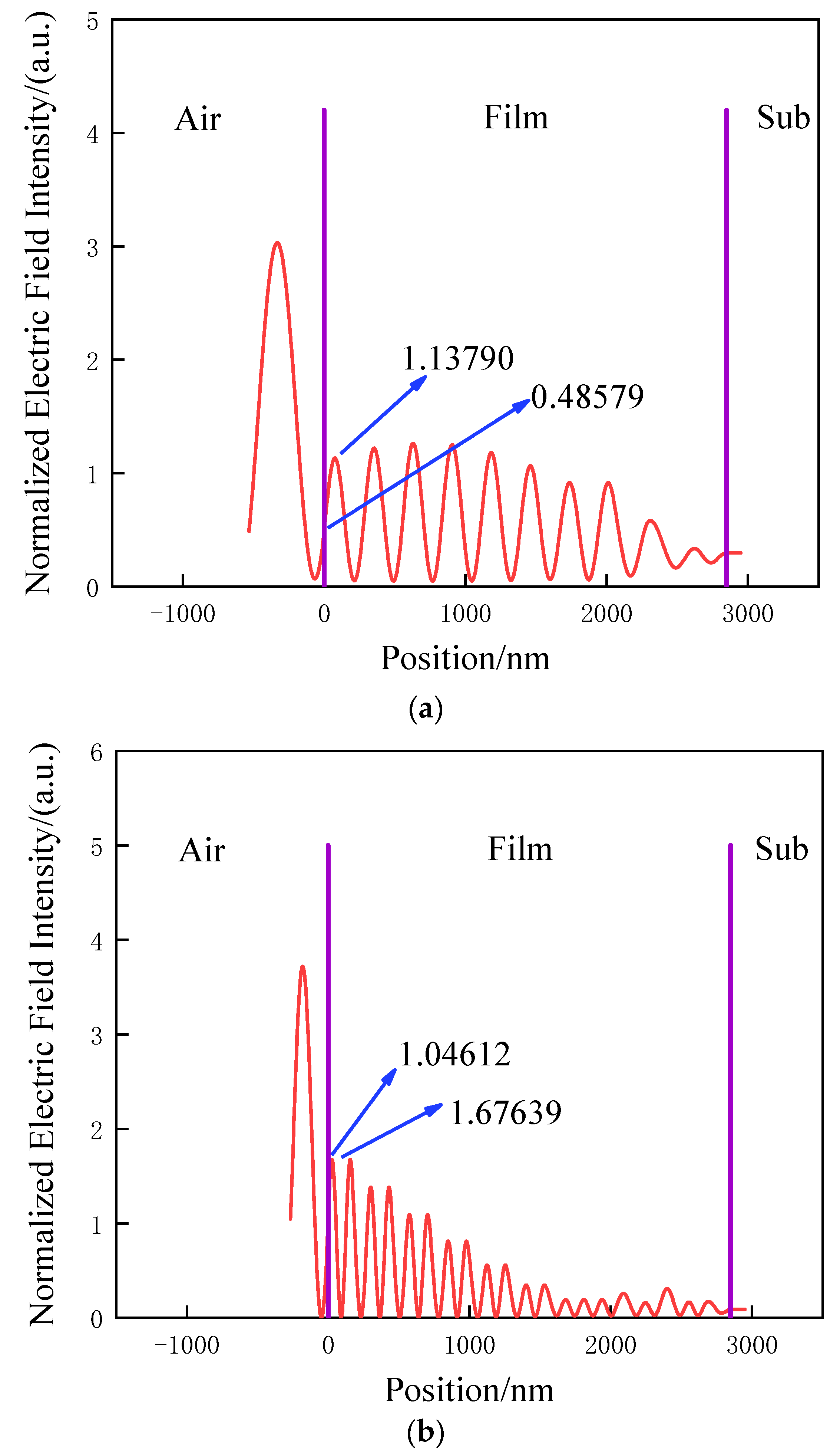
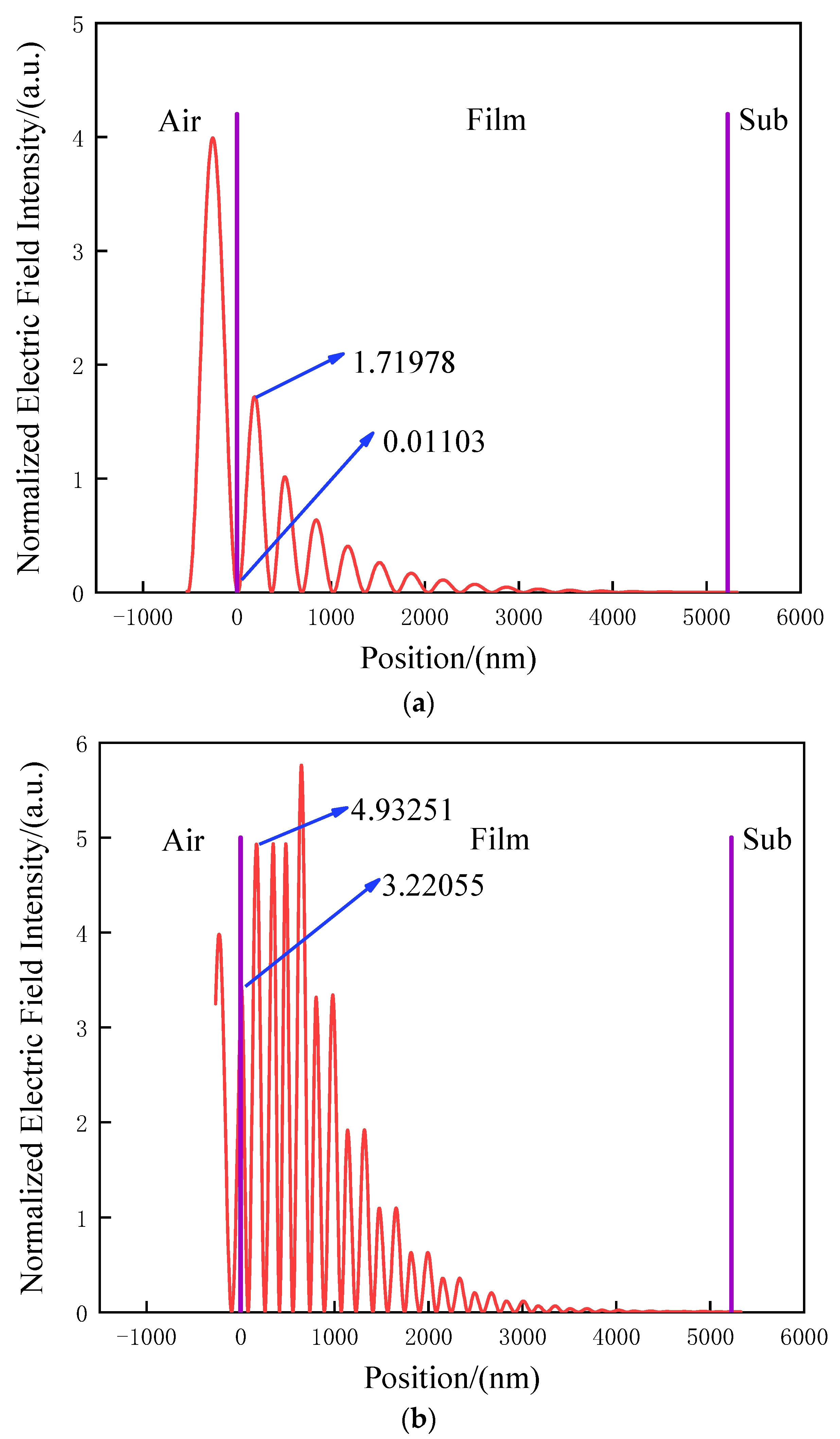
3.3. Standing-Wave Electric Field

To further analyze the laser protection performance of the non-regularized films and determine the criteria of good protection characteristics, the standing-wave electric fields of the laser protection films are discussed. The electric field intensity distributions of the samples at different laser wavelengths were calculated by the thin film design software (TFCalc), as shown in Figure 5, Figure 6 and Figure 7.
At the air–film interface, the field strength values of all samples were smaller at 1064 nm than at 532 nm. As shown in Figure 5, Figure 6 and Figure 7 and Table 2, the damage threshold of the film at 1064 nm was higher than that at 532 nm because the electric field intensity of the 1064 nm laser at the interface was lower than that of the 532 nm laser, and the outgoing photon energy of the 1064 nm laser was lower. The internal standing-wave electric field intensity distribution also directly affected the distribution of the film temperature field, with the former causing an inhomogeneous distribution of the latter, generating thermal stress and field-induced damage.
In addition, a higher standing-wave field strength in a region of uniform absorption coefficient within the film implies a higher absorption loss at that location. When the field strength is 0, the absorption loss is 0, regardless of how the absorption is changed. The greater the absorption loss, the higher the energy absorbed by the film material; as a result, more laser energy is deposited inside the film and converted to heat, causing damage to the film material by increasing its temperature. As a result, the magnitude of the laser damage resistance threshold of the laser protection film can also be controlled by adjusting the field strength value at the air–film interface, thereby controlling the laser protection capability.

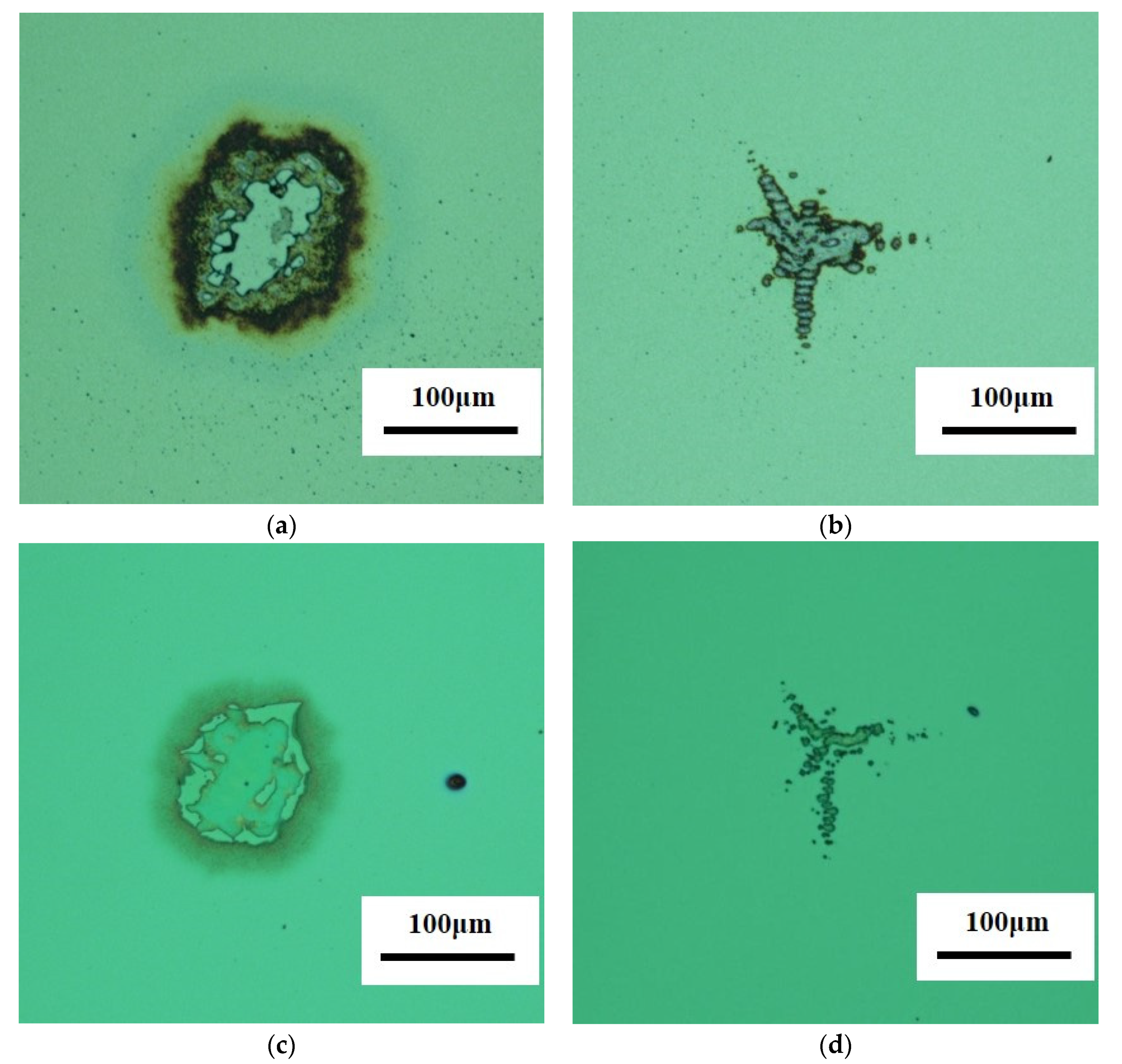
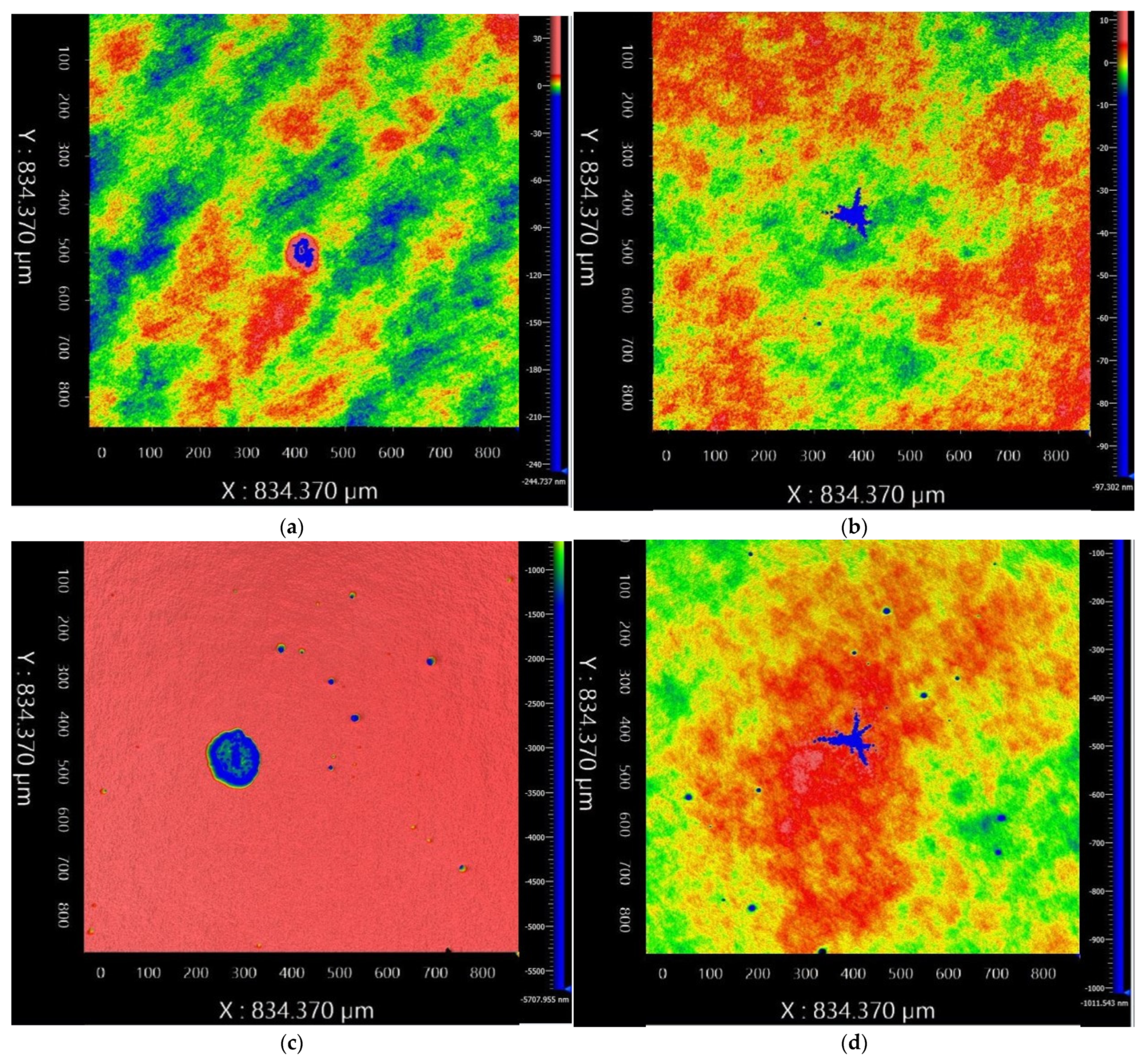
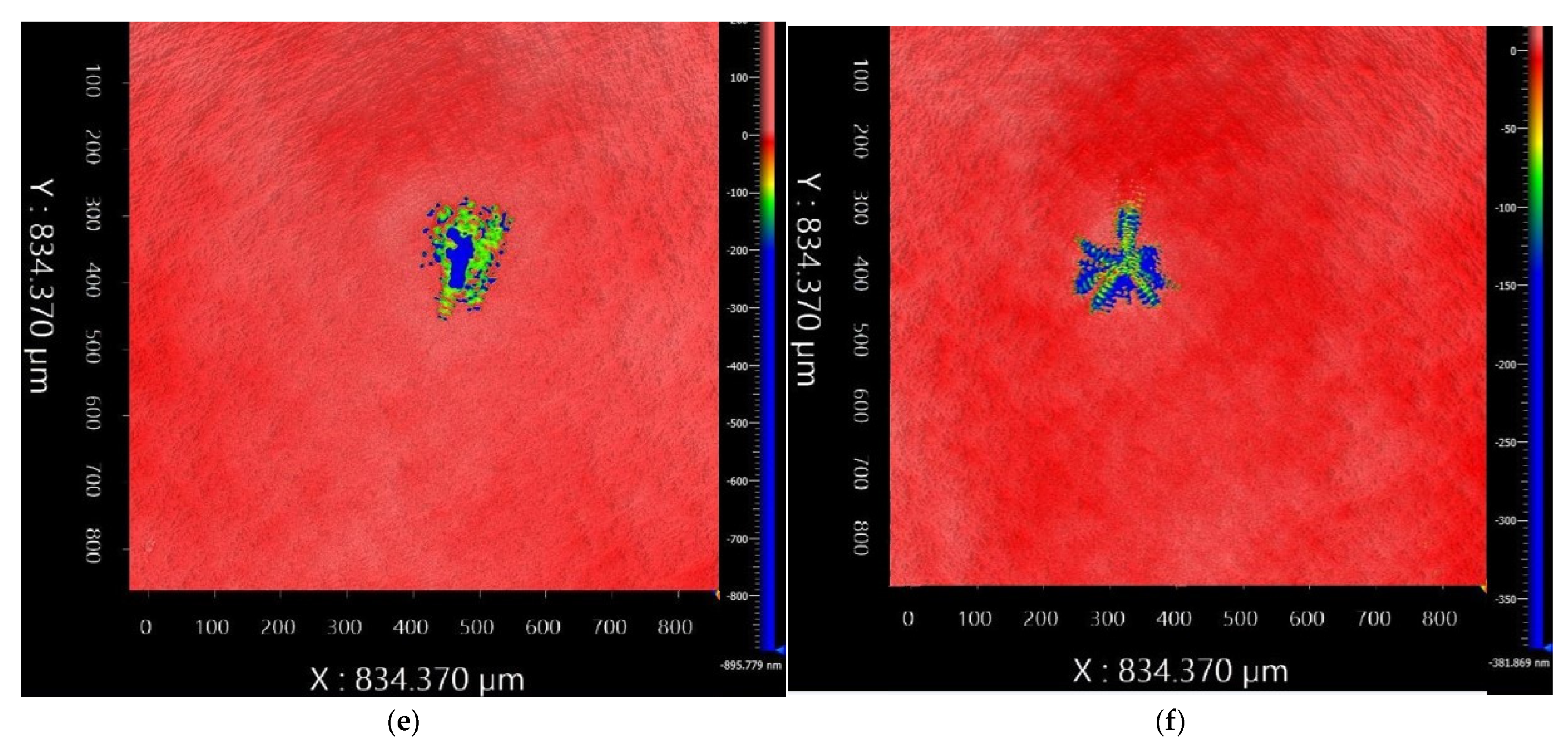
3.4. Laser Irradiation Damage Profile

3.4.1. Laser Irradiation Surface Damage Profile

To compare the laser protection performance in depth and analyze the specific effect of laser protection, a Nikon EcliPSE L150 optical microscope was used to collect the typical surface damage morphologies of the non-regularized films, as shown in Figure 8. The highly reflective TiO2/SiO2 film was more seriously ablated under the 1064 nm laser and the damaged area showed delamination because the film burns and explodes at high temperatures and spreads in all directions to form ablation marks [24]. Meanwhile, the 532 nm laser caused material spattering in the damaged area and formed irregular damage.
The HfO2/SiO2 film tended to diffuse outward under 1064 nm laser damage from the initial damage area of the film after the action of the center of the laser spot, and the diffusion area is caused by the higher temperature in the center, where heat conduction spreads the temperature to the surrounding area [25]. There was no tendency of outward diffusion at 532 nm and the involvement of field damage and black spots in the center of the damage were observed because of the presence of impurity defects in the film. Therefore, these parts were more easily damaged during laser irradiation. There were independent round damage spots near all the damaged areas owing to the porous columnar shape of the microstructure formed by thermal evaporation plating. The higher densities of the film caused a portion of the laser to sputter around the damaged area, causing new damage spots and possibly traces left by the sputtering after the defects were irradiated by the laser.
Further, the Ta2O5/SiO2 films showed damage ripples under the 1064 nm laser because of the continuous accumulation of heat conduction from the center to the surroundings. The appearance of ring damage under the 532 nm laser may be related to nodular defects, as evidenced by the sharp local temperature rise caused by laser irradiation and the presence of nodular jets inside the film causing ring-like structures [26].

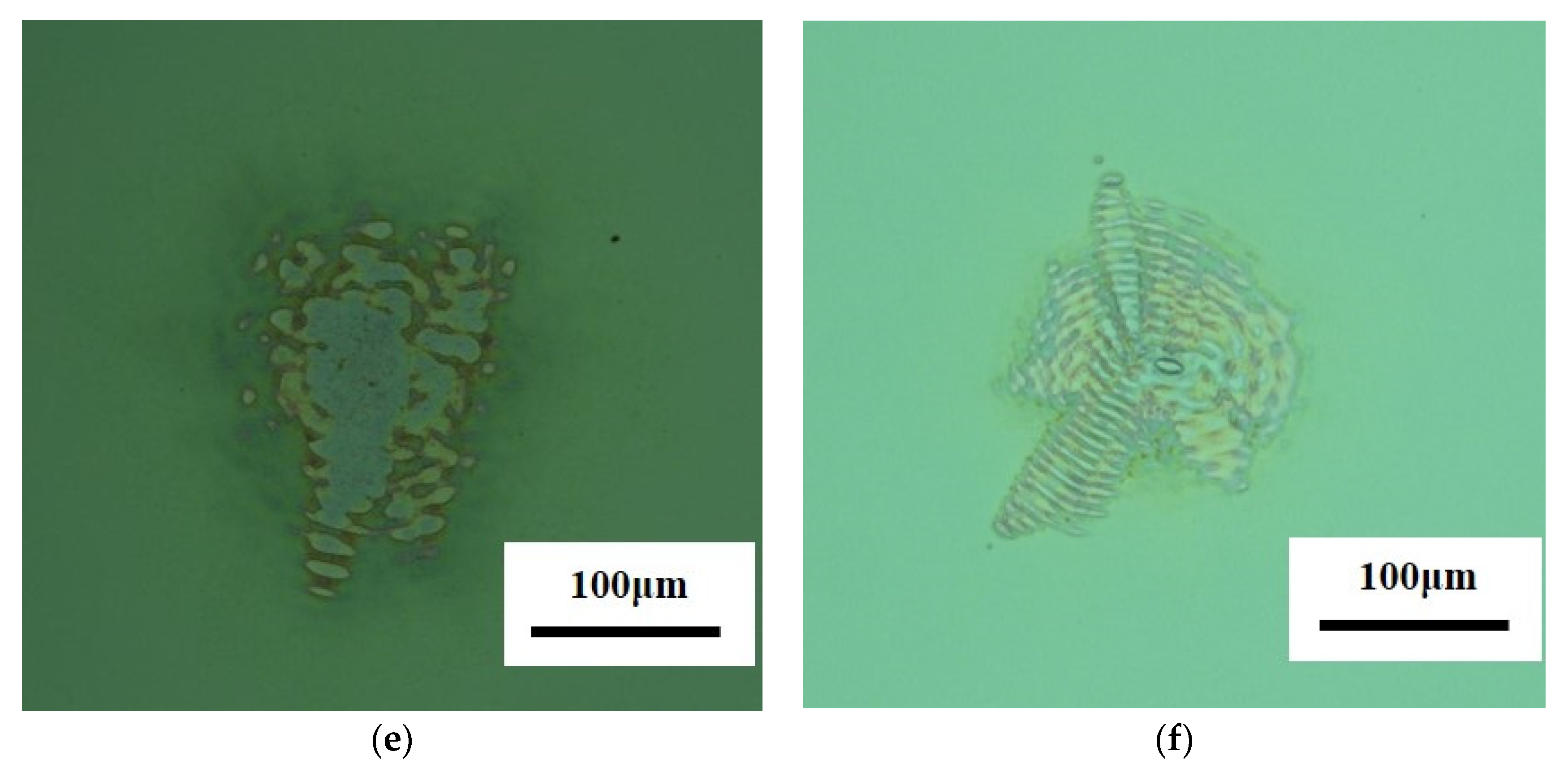
3.4.2. Three-Dimensional Laser Irradiation Damage Profile

To analyze the deep-level changes of the non-regularized films after being subjected to laser irradiation, typical three-dimensional damage morphologies were collected using a Zygo NewView 8200 interferometer (the manufacturer is Zygo Corporation of the United States), and the obtained results are shown in Figure 9. The TiO2/SiO2 films showed different degrees of damage diffusion and circular damage formed by material accumulation under irradiation at 1064 nm and 532 nm because the center of the damage was the center of the laser spot where the energy was most concentrated. After the laser action, the thin film conducts heat in all directions from the center of the damage. The molten material is impacted and propagated outward, forming a ring-like projection slightly above the film surface. The HfO2/SiO2 film showed an approximately circular depression under the 1064 nm laser and an irregular pit shape under the 532 nm laser, the damage spot depth was differentiated by the color shade, and the damage center was a flat bottom pit. The Ta2O5/SiO2 films also tended to diffuse outward at 1064 nm, which is related to thermal conduction. The depth of the damage was significantly less than the depth of the center of the damage, indicating that it was not produced by the direct action of the laser. The presence of punctate damage in the center of the damage under the 532 nm laser was due to the failure of the central part of the molten material to vaporize in a short action time and be ejected outward, which remained and crystallized in the center and formed a slight bump.

4. Conclusions

The non-regularized highly reflective TiO2/SiO2, HfO2/SiO2, and Ta2O5/SiO2 films were prepared and irradiated at 1064 nm and 532 nm to evaluate their laser protection capabilities. (1) The transmittances of the films were tested before and after irradiation and it was found that the transmittances of the three laser protection films under the 532 nm laser decreased compared with those under the 1064 nm laser, indicating that the 532 nm laser had a significant effect on film transmittance. (2) The high-energy laser protection properties of the three highly reflective films were compared at 1064 nm and 532 nm and it was found that the wavelength had a significant effect on film resistance to laser damage. The film damage threshold at 1064 nm was greater than that at 532 nm, which is related to the higher single-photon energy at 532 nm and the defect damage probability. Among them, compared to the TiO2/SiO2 and HfO2/SiO2 films, the Ta2O5/SiO2 films showed enhanced resistance to laser irradiation with laser protection properties of 9.99 J/cm2 and 4.93 J/cm2 under irradiation at 1064 nm and 532 nm, respectively. (3) The standing-wave electric field also affected the laser damage resistance of the film owing to the interface effect. Comparing the standing-wave electric field at the two wavelengths, the field strength value at the air–membrane interface of the TiO2/SiO2 film was 0.56033 lower at 1064 nm than that at 532 nm, and it was 3.20952 and 0.04492 lower at 1064 nm than that at 532 nm for the HfO2/SiO2 and Ta2O5/SiO2 films, respectively. (4) The designed laser protection films exhibited relatively better protection performance in the 1050–1080 nm band and the laser protection characteristics of the samples at 1064 nm were proved to be better than those at 532 nm. Non-regularized highly reflective high-energy laser protection films are optimally designed to meet the actual production and laser protection requirements and achieve specific optical reflection windows. The demonstrated films showed good resistance to laser damage and can simultaneously achieve laser protection in two wavelength ranges, reducing the cost of laser protection, improving the safety of laser field practitioners, and providing a basis for subsequent research on the simultaneous implementation of laser protection at multiple wavelengths.

Author Contributions

Conceptualization, X.D.; methodology, X.D. and J.S.; investigation, X.D.; data curation, X.D.; writing—original draft preparation, X.D.; writing—review and editing, J.S.; supervision, J.S.; funding acquisition, J.S. All authors have read and agreed to the published version of the manuscript.

Funding

This research was funded by the National Natural Science Foundation of China (61378050), Key Research and Development Program of Shaanxi Province (2018KWZ-02).

Institutional Review Board Statement

Not applicable.

Informed Consent Statement

Not applicable.

Data Availability Statement

Not applicable.

Conflicts of Interest

The authors declare no conflict of interest.

References

  1. Wamsley, C.E.; John, H.; Kenkel, J.M. The Role of the Laser Safety Officer and Laser Safety Programs in Clinical Practice. Aesthetic Surg. J. 2021, 41, 1550–1554. [Google Scholar] [CrossRef]
  2. Elbashar, Y.H.; Mohamed, M.A.; Rayan, D.; Badr, A.M.; Elshaikh, H.A. Optical spectroscopic analysis of bandpass filter used for laser protection based on cobalt phosphate glass. J. Opt. 2020, 49, 270–276. [Google Scholar] [CrossRef]
  3. Zhou, W.; Wu, X.; Ma, P.; Zhou, F.; Li, Z.; Niu, R.; Yang, J.; Wang, Y.; Zhang, X.; Song, Y.; et al. Enhanced ultrafast nonlinear absorption and optical limiting of indolium squaraine for laser protection. Opt. Mater. 2022, 126, 112178. [Google Scholar] [CrossRef]
  4. Tien, C.; Lin, H.; Cheng, K.; Chang, C. Design and Fabrication of Laser Protective Lenses Based on Multilayered Notch Filter with Low Residual Stress and Low Surface Roughness. Coatings 2021, 11, 1513. [Google Scholar] [CrossRef]
  5. Vasudevan, L.; Menchaca, D.I.; Tutt, J. Laser Safety Program Development at Texas A&M University—Issues and Challenges. Health Phys. 2015, 109, 205–211. [Google Scholar]
  6. Chen, Y.; Bai, T.; Dong, N.; Fan, F.; Zhang, S.; Zhuang, X.; Sun, J.; Zhang, B.; Zhang, X.; Wang, J.; et al. Graphene and its derivatives for laser protection. Prog. Mater. Sci. 2016, 84, 118–157. [Google Scholar] [CrossRef]
  7. Yang, Z.; Yang, Y.; Zhang, Y.; Guo, X.; Lu, K.; Zhang, J. High-Precision Surface Scattering Measurement System and Uncertainty Analysis Applied in Laser Protective Materials Diagnostics. Appl. Sci. 2021, 11, 9457. [Google Scholar] [CrossRef]
  8. Guo, S.; Yang, L.; Dai, B.; Geng, F.; Ralchenko, V.; Han, J.; Zhu, J. Past Achievements and Future Challenges in the Development of Infrared Antireflective and Protective Coatings. Phys. Status Solidi A 2020, 217, 2000149. [Google Scholar] [CrossRef]
  9. Zhao, D.; Xu, F.; Wang, G.; Zhang, S.; Qin, G.; Wang, B.; Han, J. SiO2/HfO2 Laser Film with Enhanced Protection and Antireflection for Sapphire Infrared Windows at High Temperatures. ACS Appl. Electron. Mater. 2021, 3, 4611–4617. [Google Scholar] [CrossRef]
  10. Li, C.; Song, S.; Gibson, D.; Child, D.; Chu, H.O.; Waddell, E. Modeling and validation of uniform large-area optical coating deposition on a rotating drum using microwave plasma reactive sputtering. Appl. Opt. 2017, 56, C65–C70. [Google Scholar] [CrossRef]
  11. Hang, L.; Liu, W.; Song, S.; Gibson, D.; Zhou, S.; Zhang, X.; Li, C.; Ahmadzadeh, S. Simulation analysis and preparation of a high optical density laser protection filter. Appl. Opt. 2020, 59, 3315–3323. [Google Scholar] [CrossRef] [PubMed]
  12. Yang, Z.; Yang, Q.; Yang, L.; Dai, B.; Xia, F.; Wang, P.; Guo, S.; Gao, G.; Xu, L.; Zhang, Y.; et al. Effect of thickness on infrared optical property of VO2 film deposited by magnetron sputtering. Sci. China Technol. Sci. 2020, 63, 1591–1598. [Google Scholar] [CrossRef]
  13. Sepúlveda, M.; Kamnev, K.; Pytlicek, Z.; Prasek, J.; Mozalev, A. Superhydrophobic−oleophobic visible−transparent antireflective nanostructured anodic HfO2 multifunctional coatings for potential solar panel applications. ACS Appl. Nano Mater. 2021, 4, 1754–1765. [Google Scholar] [CrossRef]
  14. Yin, C.; Zhu, M.; Zeng, T.; Song, C.; Chai, Y.; Shao, Y.; Zhang, R.; Zhao, J.; Li, D.; Shao, J. HfO2/SiO2 anti-reflection films for UV lasers via plasma-enhanced atomic layer deposition. J. Alloys Compd. 2021, 859, 157875. [Google Scholar] [CrossRef]
  15. Gu, J.; Wei, H.; Ren, F.; Fan, Q.; Xu, G.; Chen, X.; Song, S.; Dou, S.; Zhao, J.; Li, Y. Fabrication and performances of double-sided HfO2 anti-reflection films with ultra-high infrared transmittance. J. Alloys Compd. 2021, 858, 158337. [Google Scholar] [CrossRef]
  16. Zhang, D.; Fan, S.; Zhao, Y.; Gao, W.; Shao, J.; Fan, R.; Wang, Y.; Fan, Z. High laser-induced damage threshold HfO2 films prepared by ion-assisted electron beam evaporation. Appl. Surf. Sci. 2004, 243, 232–237. [Google Scholar] [CrossRef]
  17. Li, C.; Zhao, Y.; Cui, Y.; Wang, Y.; Peng, X.; Shan, C.; Zhu, M.; Wang, J.; Shao, J. Investigation on picosecond laser-induced damage in HfO2/SiO2 high-reflective coatings. Opt. Laser Technol. 2018, 106, 372–377. [Google Scholar] [CrossRef]
  18. Rao, K.N.; Murthy, M.A.; Mohan, S. Optical properties of electron-beam-evaporated TiO2 films. Thin Solid Films 1989, 176, 181–186. [Google Scholar] [CrossRef]
  19. Yao, J.; Fan, Z.; Jin, Y.; Zhao, Y.; He, H.; Shao, J. Investigation of damage threshold to TiO2 coatings at different laser wavelength and pulse duration. Thin Solid Films 2008, 516, 1237–1241. [Google Scholar] [CrossRef]
  20. Wolf, M.J.; Roitsch, S.; Mayer, J.; Nijmeijer, A.; Bouwmeester, H.J.M. Fabrication of ultrathin films of Ta2O5 by a sol–gel method. Thin Solid Films 2013, 527, 354–357. [Google Scholar] [CrossRef]
  21. ISO 11254-1:2000; Lasers and Laser-Related Equipment-Determination of Laser-Induced Damage Threshold of Optical Surfaces-Part1: 1-on-1 Test. International Organization for Standardization: Geneva, Switzerland, 2000.
  22. Porteus, J.O.; Seitel, S.C. Absolute onset of optical surface damage using distributed defect ensembles. Appl. Opt. 1984, 23, 3796. [Google Scholar] [CrossRef] [PubMed]
  23. Batavičiutė, G.; Grigas, P.; Smalakys, L.; Melninkaitis, A. Revision of laser-induced damage threshold evaluation from damage probability data. Rev. Sci. Instrum. 2013, 84, 045108. [Google Scholar] [CrossRef] [PubMed]
  24. Xu, J.; Chen, J.; Chen, P.; Wang, Y.; Zhang, Y.; Kong, F.; Cao, H.; Jin, Y.; Shao, J. Continuous-wave laser damage mechanism of a spectral combining grating. Appl. Opt. 2019, 58, 2551–2555. [Google Scholar] [CrossRef] [PubMed]
  25. Wang, J.; Feng, C.; Zhang, W.; Xu, Z.; Liu, X.; Yi, K.; Shao, J. Hydrophobic antireflective coating with high laser damage threshold by physical vapor deposition. Mod. Phys. Lett. B 2021, 32, 2150209. [Google Scholar] [CrossRef]
  26. Wu, B.; Bartch, U.; Jupé, M.; Jensen, L.; Lappschies, M.; Starke, K.; Ristau, D. Morphology investigations of laser induced damage. In Proceedings of the Boulder Damage Symposium XXXVIII: Annual Symposium on Optical Materials for High Power Lasers, Boulder, CO, USA, 25–27 September 2006; Volume 6403, pp. 407–416. [Google Scholar]
Figure 1. Theoretical transmittance spectra of highly reflective (a) TiO2/SiO2, (b) HfO2/SiO2, and (c) Ta2O5/SiO2 films.
Coatings 12 01614 g001aCoatings 12 01614 g001b
Figure 2. Transmission spectra of the non-regularized highly reflective TiO2/SiO2 film before and after testing at (a) 1064 nm and (b) 532 nm.
Coatings 12 01614 g002
Figure 3. Transmission spectra of the non-regularized highly reflective HfO2/SiO2 film before and after testing at (a) 1064 nm and (b) 532 nm.
Coatings 12 01614 g003
Figure 4. Transmission spectra of the non-regularized highly reflective Ta2O5/SiO2 film before and after testing at (a) 1064 nm and (b) 532 nm.
Coatings 12 01614 g004
Figure 5. Relative standing-wave electric field intensity distribution of the non-regularized highly reflective TiO2/SiO2 film at (a) 1064 nm and (b) 532 nm (The red line indicates the simulated electric field strength of the film, the purple line at the air-film interface indicates the film surface location, and the purple line at the film-substrate interface indicates the film thickness location; the value of the field strength at the interface between air and film is the interfacial electric field strength, and the first peak of the electric field strength inside the film is the peak electric field strength).
Coatings 12 01614 g005
Figure 6. Relative standing-wave electric field intensity distribution of the non-regularized highly reflective HfO2/SiO2 film at (a) 1064 nm and (b) 532 nm (The red line indicates the simulated electric field strength of the film, the purple line at the air-film interface indicates the film surface location, and the purple line at the film-substrate interface indicates the film thickness location; the value of the field strength at the interface between air and film is the interfacial electric field strength, and the first peak of the electric field strength inside the film is the peak electric field strength).
Coatings 12 01614 g006
Figure 7. Relative standing-wave electric field intensity distribution of the non-regularized highly reflective Ta2O5/SiO2 film at (a) 1064 nm and (b) 532 nm (The red line indicates the simulated electric field strength of the film, the purple line at the air-film interface indicates the film surface location, and the purple line at the film-substrate interface indicates the film thickness location; the value of the field strength at the interface between air and film is the interfacial electric field strength, and the first peak of the electric field strength inside the film is the peak electric field strength).
Coatings 12 01614 g007
Figure 8. Typical morphologies of laser protection films after laser damage: TiO2/SiO2 film at (a) 1064 nm, 5.99 J/cm2 and (b) 532 nm, 3.04 J/cm2; HfO2/SiO2 film at (c) 1064 nm, 5.89 J/cm2 and (d) 532 nm, 1.48 J/cm2; Ta2O5/SiO2 film at (e) 1064 nm, 9.99 J/cm2 and (f) 532 nm, 4.93 J/cm2.
Coatings 12 01614 g008aCoatings 12 01614 g008b
Figure 9. Typical three-dimensional damage patterns of laser protection films: TiO2/SiO2 film at (a) 1064 nm, 5.99 J/cm2 and (b) 532 nm, 3.04 J/cm2; HfO2/SiO2 film at (c) 1064 nm, 5.89 J/cm2 and (d) 532 nm, 1.48 J/cm2; Ta2O5/SiO2 film at (e) 1064 nm, 9.99 J/cm2 and (f) 532 nm, 4.93 J/cm2.
Coatings 12 01614 g009aCoatings 12 01614 g009b
Table 1. Thin film deposition process parameters.
Film MaterialsBaking Temperature/°CFilm-Forming Holding Vacuum/PaRate of Evaporation/A/s
TiO2/SiO22002.0 × 10−23.0
HfO2/SiO22002.0 × 10−23.0
Ta2O5/SiO22002.0 × 10−23.0
Table 2. Damage resistance of highly reflective laser protection films.
Sample Serial NumberHigh-Refractive-Index MaterialsLIDT (1064 nm, 10 ns)/J/cm2LIDT (532 nm, 10 ns)/J/cm2
1TiO2/SiO25.993.04
2HfO2/SiO25.891.48
3Ta2O5/SiO29.994.93
Publisher’s Note: MDPI stays neutral with regard to jurisdictional claims in published maps and institutional affiliations.

